Efficient Type II Second Harmonic Generation in an Indium Gallium Phosphide on insulator wire waveguide aligned with a crystallographic axis
Abstract
We theoretically and experimentally investigate type II second harmonic generation in III-V-on-insulator wire waveguides. We show that the propagation direction plays a crucial role and that longitudinal field components can be leveraged for robust and efficient conversion. We predict that the maximum theoretical conversion is larger than that of type I second harmonic generation for similar waveguide dimensions and reach an experimental conversion efficiency of 12 %/W, limited by the propagation loss.
Second harmonic generation (SHG) was first demonstrated almost 60 years ago [1] and still attracts a lot of attention. In particular, many novel integrated platforms for integrated SHG have recently emerged [2, 3, 4]. Conversions as high as 47000 %/(W.cm2) have been demonstrated in III-V semiconductors [5] and ultra-wide tuning was recently shown in silicon waveguides [6]. The large intrinsic nonlinearity in addition to the high-index contrast of sub-wavelength structures leads to very large effective nonlinearities. Different schemes for phase matching have been proposed and implemented [7, 8, 9]. Type I modal phase matching, consisting in engineering the waveguide cross section such that a pump mode and a SH higher-order mode propagate at the same phase velocity, is attractive because standard waveguiding structures can be used. It however leads to lower conversion efficiency as compared to other schemes because of the sub-optimal overlap between the pump and SH mode in the nonlinear core of the waveguide. Record conversions in gallium arsenide wire waveguides were recently reported by optimizing such overlap. But the efficiency is still limited because very thin layers are used to ensure phase matching between two fundamental modes [5]. Moreover, it makes the conversion very sensitive to fabrication variations.
Here we show that type II SHG can help alleviate these limitations. We theoretically analyze the nonlinear conversion with a full-vectorial model to identify the most efficient configurations and experimentally confirm our predictions in indium gallium phosphide (InGaP) nanowires.
To the best of our knowledge, type II SHG has never been demonstrated in the strong-guidance regime. It was previously studied in AlGaAs photonic wires with low vertical confinement [10], where the modes are well approximated by transverse waves. As we recently demonstrated for the case of type I SHG, more complex wave mixing involving the longitudinal components can be expected in III-V-on-insulator wire waveguides [11, 12]. We hence apply the same vectorial analysis to the case of type II phase matching in order to identify efficient nonlinear couplings between a pump around 1550 nm and a higher order mode around 775 nm.
We write the electric field as a superposition of three forward propagating bound modes, two oscillating at and one at , in the waveguide frame (), where is the horizontal coordinate, the vertical coordinate and the propagation direction (see Fig. 2). The total electric field reads:
| (1) |
where and represent the amplitudes of both pump modes and the amplitude of the SH mode (expressed in ). , are the propagation constants at the carrier frequency and is the propagation constant at the carrier frequency 2. and are the orthonormal vectorial electric profiles of the modes. They satisfy the usual orthonormality condition [13].
The propagation equations can be found through perturbation theory [14, 15, 16] . Here, we only retain the nonlinear terms involving three different modes and include the propagation loss. We find:
| (2) | ||||
where , and are the linear loss coefficients of the respective mode and is the wavenumber mismatch. The effective nonlinearity , expressed in , reads
| (3) |
with , the vacuum permittivity and , the nonlinear waveguide core. We recall that Eqs.(2) are written in the waveguide frame such that the nonlinear tensor elements are dependent on the propagation direction. In the crystal frame of a III-V semiconductor, only the elements are nonzero. To account for other directions, the nonlinear tensor must be rotated (see e.g. [10]). Most III-V wafers are grown along a crystal axis. Here we consider the case of a wafer grown along the [010] crystallographic axis and use the [100] direction as the reference in the propagation plane.
In the undepleted regime, the SH output power can be exactly calculated. We neglect the parametric down conversion terms and integrate (2) along the propagation direction. We find
| (4) |
where and . are the input powers at the pump wavelength. To maximize the conversion, we set with the total input power. The maximum output power, found by setting , can then be written , where
| (5) |
and L the length of the waveguide. This is the same expression as that of type I SHG [11]. In what follows we use the effective nonlinearity to compare different configurations as well as to confront our experimental results with theoretical predictions.
We now look for specific cases of phase matching to evaluate the theoretical conversion efficiency in standard waveguides. We first consider air-clad, fully-etched, InGaP-on-insulator wire waveguides. The single nonzero second order nonlinear coefficient was measured to be as high as pm/V [17]. In principle, any two pump modes can be used for type II SHG, but wave mixing processes involving the two fundamental modes (TE00 and TM00) are expected to be the most efficient. Moreover, it is the easiest scheme to implement experimentally
in sub-wavelength waveguides with free-space injection. We hence look for phase matching between the two fundamental modes around 1550 nm and a higher-order mode around 775 nm. We vary the width and height of the waveguide in steps of 5 nm in each direction. When a phase matching point is found in a 10 nm window around the 1550 nm wavelength, we compute the efficiency as a function of the propagation direction (either or ) and place a marker in the efficiency map shown in Fig. 1.
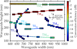
The marker color codes the relative strength of the coupling and its shape indicates the propagation direction for which it is maximized: squares correspond to 0∘ waveguides while diamonds represent 45∘ waveguides. To limit the computational time, we restrict the simulations to widths between 600 and 1000 nm and heights between 100 and 400 nm. We connect the markers corresponding to the same SH higher-order mode with a line. Interestingly, and in contrast to type I SHG [12], the most efficient conversion occurs for relatively thick waveguides (620 nm wide, 300 nm high) aligned with a main crystallographic axis []. For comparison, the maximum found for type I SHG in the same range of waveguide dimensions is [12]. The larger efficiency for type II SHG can be understood by analyzing the expression of the effective nonlinearity for waves propagating along a crystallographic axis of a III-V material. It reads
| (6) |
where is the single nonzero tensor element of InGaP. In the specific case of predominant TM00 and TE00 pump modes and a TM higher-order mode at the SH, (6) can be approximated by the simpler expression:
| (7) |
The effective nonlinearity is dominated by two terms, both involving a longitudinal electric field component. A transverse mode approximation would yield no conversion in this case. The wave mixing process involving longitudinal components does not preclude efficient conversion because, in high index contrast platforms, the longitudinal components can be almost as large as their transverse counterpart [18]. Importantly, longitudinal components have a spatial distribution that is distinct from, but linked to, that of the principal transverse component [13]. In the case of phase matching to a TM01 mode, both terms of (7) are large because the involved spatial distributions are very similar to each other. This is made possible by the very large index contrast of the platform and highlights the strong potential of type II phase matching for SHG in III-V-on-insulator wire waveguides.
Next we aim to experimentally confirm this large theoretical conversion efficiency.

We fabricate InGaP on insulator waveguides through wafer bonding [19]. The starting epitaxial stack is made of a 350 µm substrate of AlGaAs, a 200 nm sacrificial layer of InGaP, another 200 sacrificial layer of AlGaAs and then a 320 nm InGaP layer. A thin layer of 15 nm of silicon oxide is deposited on top of the stack to improve adhesion. The stack is then bonded on a oxidized silicon wafer (3 µm SiO2) using a BenzoCycloButene (BCB) dilution as an adhesive layer. We remove the substrate with a solution in a 1:4:1 proportion and pattern waveguides using electron-beam lithography. A negative resist [hydrogen silsesquioxane (HSQ)] is deposited prior to illumination. The waveguides are patterned using ICP etching. The electron-beam resist is not removed resulting in a 200 nm cladding with an index similar to that of silicon dioxide (see Fig. 2).
The width of the waveguides, characterized with scanning electron microscopy, is 850 nm. In this structure, the efficient conversion to a TM01 SH mode, as discussed above, is predicted to occur for a pump wavelength of 1536 nm (see Fig. 2). The corresponding theoretical effective nonlinearity is . We design waveguides made of three sections of different directions [see Fig. 3(b)]. This is because the cleave direction of both silicon and III-V semiconductors are at 45∘ (i.e. along the [101] and [] axis). The main section, located in the middle, is aligned with a crystal axis. It is connected, on both ends, to sections normal to cleavage planes to facilitate light injection and collection. A 5 µm wide and 200 µm long taper is used at the input to optimize the injection. The middle section is 1.4 mm long and the total length is 4.5 mm.
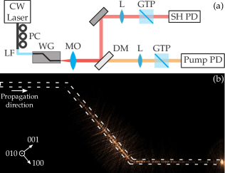
The experimental setup is depicted in Fig. 3(a). We inject the light using a lensed fiber. The coupling loss is estimated at 6 dB. A polarization controller allows us to tune the input polarization state. The light is collected from the waveguide with a high NA objective (0.9). The pump and second harmonic wavelengths are separated with a dichroic mirror and sent, through a Glan-Taylor polarizer, to a photodiode. To characterize the SH diffusion pattern, we image the chip from the top with a silicon camera. In a first experiment, we inject 25 mW from a C-band laser and tune both the input wavelength and polarization. As predicted, the brightest pattern is found at 1536 nm when both a TE00 and a TM00 pump mode are simultaneously excited. The output SH wave is predominantly vertically polarized, as expected. The corresponding SH diffusion pattern is shown in Fig. 3(b). We see that the SH appears at the beginning of the middle section, the one aligned with a crystallographic axis. The SH intensity increases until the second bend, after which it decays, as expected from the lack of nonlinear coupling in waveguides rotated at 45∘ from a crystal axis. To extract the experimental effective nonlinearity (), we estimate the loss at each wavelength by fitting diffusion patterns. For the pump modes, we perform an experiment at low power and for the SH TM01 mode we use the last section of the waveguide where no SH conversion occurs. We find 1.2 dB/mm for the pump modes and 6.4 dB/mm at the second harmonic, corresponding to µm. An injected input power of 25 mW corresponds to 3.8 mW at the beginning of the 0∘ section. Because it is difficult to experimentally evaluate the outcoupling loss for the SH mode, we consider that we collect all the output power and hence give a lower bound of the experimental effective nonlinearity. We first extract from the output SH power at the phase matching wavelength and next characterize the spectral transmittance of the process.
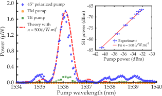
The maximum output SH power (at as a function of the input power is shown in the inset of Fig. 4. It is fitted with the theoretical function that allows us to extract the conversion efficiency value. We find . The recorded output SH power as a function of input wavelength for three different input polarization states is shown in Fig. 4 and confirms that the process is more efficient when both input modes are equally excited. Also plotted is the theoretical transfer function (4) computed for . The agreement between the theoretical spectral acceptance and our experimental results is excellent.
The maximum conversion efficiency, defined as , is equal to 2500 %/(W.cm2), which corresponds to 12 %/W in our waveguide. It is larger than recently reported values in lithium niobate [41 %/(W.cm2)] [20] and gallium phosphide [0.3 %/(W.cm2)] [21]. It is however an order of magnitude lower than the record 47000 %/(W.cm2) efficiency recently obtained in GaAs nanowaveguides [5]. Yet, the theoretical limit in our case, corresponding to , is 102400 %/(W.cm2). It highlights the strong potential of type II SHG for future integrated frequency converters. InGaP wire waveguides with much lower propagation loss should hence permit converting as little as 1 µW into 1 nW of SH power in a 1 cm long waveguide. Encouragingly, several demonstrations of low loss III-V semiconductor waveguides have been recently reported [22, 23].
In conclusion, we demonstrated efficient type II SHG in InGaP nanowires. We performed a full-vectorial theoretical analysis and showed that the most efficient conversion occurs in waveguides aligned with a crystallographic axis. In that configuration, the nonlinear coupling is enabled by longitudinal field components of both a pump mode and the SH mode. We confirmed our prediction experimentally by demonstrating very efficient conversion in a 850 nm wide, 320 nm thick wire waveguide. As predicted, the conversion is maximized when the two fundamental modes at the pump wavelength are equally excited and the conversion occurs in a waveguide aligned with a main crystallographic axis. These results demonstrate the potential of type II phase matching to maximize the conversion in III-V semiconductor nanowaveguides, which we expect to play a role in future quantum circuits [24] and frequency comb stabilization devices [25, 26].
Disclosures. The authors declare no conflicts of interest.
References
- [1] P. A. Franken, A. E. Hill, C. W. Peters, and G. Weinreich. Generation of Optical Harmonics. Physical Review Letters, 7(4):118–119, August 1961.
- [2] Katharina Schneider, Pol Welter, Yannick Baumgartner, Herwig Hahn, Lukas Czornomaz, and Paul Seidler. Gallium Phosphide-on-Silicon Dioxide Photonic Devices. Journal of Lightwave Technology, 36(14):2994–3002, July 2018.
- [3] Jacob S. Levy, Mark A. Foster, Alexander L. Gaeta, and Michal Lipson. Harmonic generation in silicon nitride ring resonators. Optics Express, 19(12):11415, June 2011.
- [4] Alan D. Logan, Michael Gould, Emma R. Schmidgall, Karine Hestroffer, Zin Lin, Weiliang Jin, Arka Majumdar, Fariba Hatami, Alejandro W. Rodriguez, and Kai-Mei C. Fu. 400%/W second harmonic conversion efficiency in 14 um-diameter gallium phosphide-on-oxide resonators. Optics Express, 26(26):33687, December 2018.
- [5] Eric J. Stanton, Jeff Chiles, Nima Nader, Galan Moody, Nicolas Volet, Lin Chang, John E. Bowers, Sae Woo Nam, and Richard P. Mirin. Efficient second harmonic generation in nanophotonic GaAs-on-insulator waveguides. Optics Express, 28(7):9521, March 2020.
- [6] Neetesh Singh, Manan Raval, Alfonso Ruocco, and Michael R. Watts. Broadband 200-nm second-harmonic generation in silicon in the telecom band. Light: Science & Applications, 9(1):17, December 2020.
- [7] Moritz Bartnick, Matteo Santandrea, Jan Philipp Hoepker, Frederik Thiele, Raimund Ricken, Viktor Quiring, Christof Eigner, Harald Herrmann, Christine Silberhorn, and Tim J. Bartley. Cryogenic second harmonic generation in periodically-poled lithium niobate waveguides. arXiv:2005.07500 [physics, physics:quant-ph], May 2020. arXiv: 2005.07500.
- [8] Cheng Wang, Carsten Langrock, Alireza Marandi, Marc Jankowski, Mian Zhang, Boris Desiatov, Martin M. Fejer, and Marko Loncar. Ultrahigh-efficiency second-harmonic generation in nanophotonic PPLN waveguides. Optica, 5(11):1438, November 2018. arXiv: 1810.09235.
- [9] Edgars Nitiss, Tianyi Liu, Davide Grassani, Martin Pfeiffer, Tobias J. Kippenberg, and Camille-Sophie Brès. Formation Rules and Dynamics of Photoinduced chi(2) Gratings in Silicon Nitride Waveguides. ACS Photonics, 7(1):147–153, January 2020.
- [10] D. Duchesne, K. A. Rutkowska, M. Volatier, F. Légaré, S. Delprat, M. Chaker, D. Modotto, A. Locatelli, C. De Angelis, M. Sorel, D. N. Christodoulides, G. Salamo, R. Arès, V. Aimez, and R. Morandotti. Second harmonic generation in AlGaAs photonic wires using low power continuous wave light. Optics Express, 19(13):12408, June 2011.
- [11] Nicolas Poulvellarie, Utsav Dave, Koen Alexander, Charles Ciret, Maximilien Billet, Carlos Mas Arabi, Fabrice Raineri, Sylvain Combrié, Alfredo De Rossi, Gunther Roelkens, Simon-Pierre Gorza, Bart Kuyken, and François Leo. Second-harmonic generation enabled by longitudinal electric-field components in photonic wire waveguides. Physical Review A, 102(2):023521, August 2020.
- [12] Charles Ciret, Koen Alexander, Nicolas Poulvellarie, Maximilien Billet, Carlos Mas Arabi, Bart Kuyken, Simon-Pierre Gorza, and François Leo. Influence of longitudinal mode components on second harmonic generation in III-V-on-insulator nanowires. Optics Express, 28(21):31584, October 2020.
- [13] Allan Whitenack Snyder and John Love. Optical Waveguide Theory. Chapman and Hall, November 1983.
- [14] Shahraam Afshar V. and Tanya M. Monro. A full vectorial model for pulse propagation in emerging waveguides with subwavelength structures part I: Kerr nonlinearity. Optics Express, 17(4):2298, February 2009.
- [15] L. Alloatti, D. Korn, C. Weimann, C. Koos, W. Freude, and J. Leuthold. Second-order nonlinear silicon-organic hybrid waveguides. Optics Express, 20(18):20506, August 2012.
- [16] M. Kolesik and J. V. Moloney. Nonlinear optical pulse propagation simulation: From Maxwell’s to unidirectional equations. Physical Review E, 70(3):036604, September 2004.
- [17] Yoshiyasu Ueno, Vincent Ricci, and George I Stegeman. Second-order susceptibility of Ga0.5In0.5P crystals at 1.5 um and their feasibility for waveguide quasi-phase matching. Journal of the Optical Society of America B, page 9, 1997.
- [18] Jeffrey B. Driscoll, Xiaoping Liu, Saam Yasseri, Iwei Hsieh, Jerry I. Dadap, and Richard M. Osgood. Large longitudinal electric fields (E_z) in silicon nanowire waveguides. Optics Express, 17(4):2797, February 2009.
- [19] Utsav D. Dave, Bart Kuyken, François Leo, Simon-Pierre Gorza, Sylvain Combrie, Alfredo De Rossi, Fabrice Raineri, and Gunther Roelkens. Nonlinear properties of dispersion engineered InGaP photonic wire waveguides in the telecommunication wavelength range. Optics Express, 23(4):4650, February 2015.
- [20] Cheng Wang, Xiao Xiong, Nicolas Andrade, Vivek Venkataraman, Xi-Feng Ren, Guang-Can Guo, and Marko Lončar. Second harmonic generation in nano-structured thin-film lithium niobate waveguides. Optics Express, 25(6):6963, March 2017.
- [21] Aravind P. Anthur, Zhang Haizhong, Yuriy Akimov, Ong Junrong, Dmitry Kalashnikov, Arseniy I. Kuznetsov, and Leonid Krivitsky. Second Harmonic Generation in Gallium Phosphide Nano-Waveguides. arXiv:2001.06142 [physics], January 2020. arXiv: 2001.06142.
- [22] Luisa Ottaviano, Minhao Pu, Elizaveta Semenova, and Kresten Yvind. Low-loss high-confinement waveguides and microring resonators in AlGaAs-on-insulator. Optics Letters, 41(17):3996, September 2016.
- [23] Lin Chang, Weiqiang Xie, Haowen Shu, Qi-Fan Yang, Boqiang Shen, Andreas Boes, Jon D. Peters, Warren Jin, Chao Xiang, Songtao Liu, Gregory Moille, Su-Peng Yu, Xingjun Wang, Kartik Srinivasan, Scott B. Papp, Kerry Vahala, and John E. Bowers. Ultra-efficient frequency comb generation in AlGaAs-on-insulator microresonators. Nature Communications, 11(1):1331, December 2020.
- [24] Sebastian Zaske, Andreas Lenhard, Christian A. Keßler, Jan Kettler, Christian Hepp, Carsten Arend, Roland Albrecht, Wolfgang-Michael Schulz, Michael Jetter, Peter Michler, and Christoph Becher. Visible-to-Telecom Quantum Frequency Conversion of Light from a Single Quantum Emitter. Physical Review Letters, 109(14):147404, October 2012.
- [25] Scott A. Diddams, David J. Jones, Jun Ye, Steven T. Cundiff, John L. Hall, Jinendra K. Ranka, Robert S. Windeler, Ronald Holzwarth, Thomas Udem, and T. W. Hänsch. Direct Link between Microwave and Optical Frequencies with a 300 THz Femtosecond Laser Comb. Physical Review Letters, 84(22):5102–5105, May 2000.
- [26] Yoshitomo Okawachi, Mengjie Yu, Boris Desiatov, Bok Young Kim, Tobias Hansson, Marko Lončar, and Alexander L. Gaeta. On-chip self-referencing using integrated lithium niobate waveguides. arXiv:2003.11599 [physics], March 2020. arXiv: 2003.11599.