Observation of quantum spin Hall states in Ta2Pd3Te5
Abstract
Two-dimensional topological insulators (2DTIs), which host the quantum spin Hall (QSH) effect, are one of the key materials in next-generation spintronic devices. To date, experimental evidence of the QSH effect has only been observed in a few materials, and thus, the search for new 2DTIs is at the forefront of physical and materials science. Here, we report experimental evidence of a 2DTI in the van der Waals material Ta2Pd3Te5. First-principles calculations show that each monolayer of Ta2Pd3Te5 is a 2DTI with weak interlayer interactions. Combined transport, angle-resolved photoemission spectroscopy, and scanning tunneling microscopy measurements confirm the existence of a band gap at the Fermi level and topological edge states inside the gap. These results demonstrate that Ta2Pd3Te5 is a promising material for fabricating spintronic devices based on the QSH effect.
Two-dimensional topological insulators (2DTIs), also known as quantum spin Hall (QSH) insulators, feature a bulk band gap and helical in-gap states at the material boundaries HasanMZ2010 ; QiXL2011 ; AndoY2013 . The edge states of a 2DTI can serve as one-dimensional conducting channels in which backscattering is forbidden by time-reversal symmetry. Therefore, 2DTIs provide an ideal platform to fabricate low-dissipation spintronic devices. To date, 2DTIs have only been realized in two types of materials. The first type is quantum well systems, including HgTe/CdHgTe KonigM2007 and InAs/GaSb LiuC2008 ; KnezI2011 ; DuL2015 . However, the material synthesis of these quantum wells is extremely challenging, and experimental signatures of the QSH effect have only been observed by a few research groups. The second type of 2DTI has been reported in several two-dimensional (2D) materials, such as bilayer Bi YangF2012 ; DrozdovIK2014 , monolayer 1T′ WTe2 TangS2017 ; JiaZ2017 ; PengL2017 , and graphene-like honeycomb lattices ZhuF2015 ; ReisF2017 ; DengJ2018 ; XuC2018 ; ZhuSY2019 . However, despite the large number of 2D materials as candidate 2DTIs, transport evidence of the QSH effect has only been reported in monolayer 1T′ WTe2 FeiZ2017 ; WuS2018 ; ShiY2019 .
Realizing QSH states in van der Waals materials, such as WTe2, offers great opportunities to fabricate quantum transport devices, as monolayer or few-layer materials for realizing the QSH effect are very easy to obtain. However, as a prototypical van der Waals material, 1T′ WTe2 was confirmed to be a 2DTI only in the monolayer limit WuS2018 . In bulk form, WTe2 becomes a metal with zero energy gap AliMN2014 ; SoluyanovAA2015 . As a result, QSH states disappear in multilayer WTe2 because of the hybridization of the bulk and edge states. Therefore, QSH devices based on WTe2 suffer from easy degradation of monolayer samples under ambient conditions. Since multilayer materials are typically more inert and have higher tunability via the thickness or twist angles, realizing QSH states in multilayer materials is highly desirable. This requires a semiconducting van der Waals material that hosts a similar inverted gap as the monolayer.
In this work, we report the observation of QSH states in the van der Waals material Ta2Pd3Te5 NieS2020 , which hosts a band gap in both the bulk and monolayer forms. We synthesize Ta2Pd3Te5 single crystals and investigate their electronic structures by combined first-principles calculations, transport, angle-resolved photoemission spectroscopy (ARPES), and scanning tunneling microscopy/spectroscopy (STM/STS) measurements. We prove that Ta2Pd3Te5 hosts a band gap at the Fermi level. Because of the weak interlayer coupling, the topmost layer of Ta2Pd3Te5 can be viewed as a monolayer material placed on a single-crystal substrate. As expected, we directly observe topological edge states using STS. These results provide strong evidence for QSH states in Ta2Pd3Te5. The discovery of QSH states in van der Waals materials with a significant band gap could pave the way to realizing practical QSH devices.
Ta2Pd3Te5 single crystals were synthesized by the self-flux method. The starting materials of Ta (99.999%), Pd (99.9999%), and Te (99.9999%) were mixed in an Ar-filled glove box at a molar ratio of Ta:Pd:Te=2:4.5:7.5. The mixture was placed in an alumina crucible and sealed in an evacuated quartz tube. The tube was heated to 950 ∘C over 10 h and maintained at this temperature for 2 days. Then, the tube was slowly cooled to 800 ∘C at a rate of 0.5 ∘C/h. Finally, the extra flux was removed by centrifugation at 800 ∘C. After centrifugation, single crystals of Ta2Pd3Te5 could be selected from the remnants in the crucible. To investigate the crystalline structure, single-crystal X-ray diffraction (XRD) was carried out at 273 K using Mo radiation ( = 0.71073 Å). The crystalline structure was refined by the full-matrix least-squares method on F2 by using the SHELXL-2018/3 program. Electrical resistivity () measurements were carried out on a physical property measurement system (PPMS, Quantum Design Inc.) using a standard dc four-probe technique.
ARPES experiments were performed at beamline BL-1 of the Hiroshima synchrotron radiation center IwasawaH2017 . The clean surfaces required for the ARPES measurements were obtained by cleaving the samples in an ultrahigh vacuum chamber with a base pressure of 1.010-9 Pa. Both the cleavage process and ARPES measurements were performed at 30 K. The energy resolution of the ARPES measurements was approximately 15 meV. STM/STS experiments were carried out in a home-built low-temperature (5 K) STM system with a base pressure of 210-8 Pa. The clean surfaces for STM/STS measurements were also obtained by cleaving the samples in situ at low temperature.
First-principles calculations were performed within the framework of the projector augmented wave (PAW) method Blochl1994 ; Kresse1999 implemented in the Vienna ab initio simulation (VASP) package KresseG1996 ; KresseG1996prb . The Perdew-Burke-Ernzerhof (PBE) generalized gradient approximation (GGA) exchange-correlation functional PerdewJP1996 was implemented in the calculations. The cutoff energy for plane wave expansion was 500 eV. Spin-orbit coupling was self-consistently taken into account within the second variational method. A 4-unit-cell slab structure (with 20 Å vacuum) was built to simulate the surface spectrum.
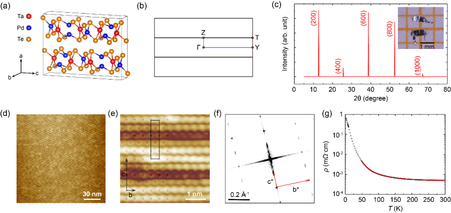
Ta2Pd3Te5 crystallizes in an orthorhombic structure with the space group Pnma (No. 62). Schematic drawings of the atomic structure and Brillouin zones (BZs) of Ta2Pd3Te5 are shown in Figs. 1(a) and 1(b), respectively. Each unit cell contains two Ta2Pd3Te5 monolayers, which are stacked along the direction via weak van der Waals interactions. Each monolayer contains a Ta-Pd mixed layer sandwiched between two Te layers. Figure 1(c) shows the XRD spectrum on a flat surface of Ta2Pd3Te5, whereby only peaks are observed. A photograph of a typical Ta2Pd3Te5 crystal is displayed in the inset of Fig. 1(c). The picture shows that the crystal is as large as 1 mm and has shiny surfaces, indicating the high crystallinity of our samples. The lattice parameters of Ta2Pd3Te5 determined from the XRD data are a = 13.9531(6) Å, b = 3.7038(2) Å, and c = 18.5991(8) Å. Figure 1(d) shows a large-scale STM image of Ta2Pd3Te5 (the bc plane). The surface is slightly corrugated, forming periodic stripes along the b direction. A zoomed-in STM image with atomic resolution is displayed in Fig. 1(e). Each bright protrusion corresponds to a Te atom, which well matches the structure model of Ta2Pd3Te5. From the STM image, the rectangular structure of the bc plane of Ta2Pd3Te5 can also be identified in the fast Fourier transformed image in Fig. 1(e). The lattice constants determined from our STM results are 3.6 Å and 18.7 Å, respectively, which agree well with the lattice constants along the and directions.
The temperature dependence of the electrical resistivity of Ta2Pd3Te5 is displayed in Fig. 1(g). When the temperature is decreased from 300 K to 2 K, the resistivity increases monotonically, indicating semiconductor behavior. The temperature-dependent resistivity can be fitted with the Arrhenius model exp(/), where and are the Boltzmann constant and thermal activation energy, respectively. The fitting results are shown by the red line in Fig. 1(g). The fitted is approximately 14 meV. Therefore, bulk Ta2Pd3Te5 is a narrow-gap semiconductor with a global band gap of 14 meV.
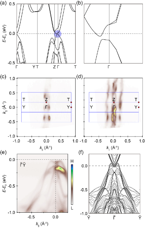
Before showing further experimental results of Ta2Pd3Te5, we briefly discuss the topological properties based on our first-principles calculation results. For bulk Ta2Pd3Te5, the symmetry indicators () are 0. However, it has a nontrivial mirror Chern number in the plane due to the band inversion at the point NieS2020 , which indicates the topological nature of bulk Ta2Pd3Te5. In the monolayer limit, Ta2Pd3Te5 becomes a 2DTI NieS2020 with a similar band inversion. Its nontrivial topology has also been confirmed by the one-dimensional Wilson loop method. Figure 2(a) shows the band structure of monolayer Ta2Pd3Te5, where an inverted band gap near the Fermi level can be identified. The calculated gap along the –Z direction is approximately 5 meV. Notably, the gap fitted based on our transport measurements (14 meV) on bulk samples is larger than the calculated value. We will later show that our STS measurements also indicate a significantly larger gap compared to the calculation results. This inconsistency probably originates from the fact that density functional theory (DFT) calculations may underestimate the band gap of materials.
To study the electronic structure of Ta2Pd3Te5, we performed ARPES measurements on a freshly cleaved surface. An ARPES intensity map of the Fermi surface is displayed in Fig. 2(c), which shows a weak spectral weight along the – direction. Because of the large lattice constant along the c direction, we observed four BZs along –. With increasing binding energy, an oval-like pocket appears at the point, as shown in Fig. 2(d). The band structure along the – direction is shown in Fig. 2(e), which agrees well with our slab calculation results (see Fig. 2(f)). These ARPES results, combined with the DFT calculations, provide strong evidence of the topological band structure of Ta2Pd3Te5.
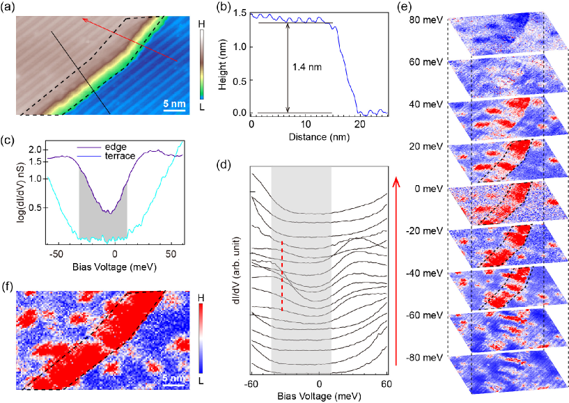
Now that we have shown the existence of a topological band structure and a band gap in Ta2Pd3Te5, we proceed to studying the topological edge states, which are a key signature of the QSH state in monolayer Ta2Pd3Te5. Because of the weak interlayer coupling, topological edge states are expected to exist at the periphery of the topmost layers. An ideal technique to study the edge states is STS because the tunneling conductance is proportional to the local density of states (LDOS). Figure 3(a) shows an STM image that contains a step edge. From the line profile in Fig. 3(b), the step height is 1.4 nm, which corresponds to the lattice constant along the direction. Figure 3(c) shows the dI/dV curves taken on the flat terrace and near the step edge. On the flat terrace, we observe a band gap at the Fermi level, in agreement with the semiconductor behavior of Ta2Pd3Te5. The estimated gap size is approximately 43 meV, with the valence band top and conduction band bottom at -33 meV and 10 meV, respectively. The band gap shows negligible variation across the flat terrace, despite the height variation of the Te chains, as shown in Supplementary Fig. S1. This indicates the high spatial homogeneity of the surface, which provides further evidence for the global nature of the band gap. Notably, the gap estimated from our STS data is larger than that fitted based on the transport measurements. This may originate from the surface sensitivity of the STS technique, which indicates a larger band gap in monolayer Ta2Pd3Te5 than in the bulk material. Near the step edge, however, the LDOS is dramatically enhanced, featuring a V-shape in the energy range between -40 and 40 meV. This indicates the existence of edge states inside the band gap. To better visualize the evolution of the edge states, we present a series of dI/dV curves across the step edge in Fig. 3(d). When the tip approaches the step edge, the tunneling conductance inside the gap gradually increases, as indicated by the red dashed line in Fig. 3(d).
To confirm the spatial distribution of the edge states, we performed real space dI/dV mapping, as shown in Fig. 3(e). When the bias voltage is set to be within the band gap (e.g., 0 and -20 mV), the tunneling conductance is dramatically enhanced near the step edge. The enhancement of the tunneling conductance vanishes at bias voltages outside the band gap, resulting in a uniform LDOS over the entire surface (e.g., at 80 mV). Figure 3(f) shows an averaged dI/dV map at several bias voltages that span the band gap, where the enhancement of the LDOS near the step edge can be clearly seen. The fact that these edge states are located inside the gap agrees well with their topological nature. Notably, the step edge is not straight and contains several different terminations. Nevertheless, edge states always exist, despite the slight variation in the details of the STS spectra. This provides strong evidence for the robustness of the edge states, which is also consistent with their topological nature NieS2020 . Similar topological edge states have been reported in several other topological materials, such as ZrTe5 WuR2016 and TaIrTe4 DongX2019 .
In summary, our results support the existence of significant inverted gap and topological edge states in the van der Waals material Ta2Pd3Te5, thus providing strong evidence for QSH states in Ta2Pd3Te5. In stark contrast to WTe2, multilayer and even bulk Ta2Pd3Te5 hosts a similar inverted gap at the Fermi level. This is beneficial for device applications because multilayer samples are typically more inert and have higher tunability. Therefore, we expect that Ta2Pd3Te5 will become a promising material for fabricating QSH devices.
Acknowledgments
This work was supported by the Ministry of Science and Technology of China (Grants No. 2018YFE0202700, No. 2017YFA0302901, No. 2016YFA0300604, and No. 2016YFA0300904), the National Natural Science Foundation of China (Grants No. 11974391, No. 11974395, No. U2032204, No. 11774399, No. 11825405, and No. 1192780039), the Beijing Natural Science Foundation (Grants No. Z180007 and No. Z180008), the Strategic Priority Research Program of the Chinese Academy of Sciences (Grants No. XDB33030100 and No. XDB30000000), and the K. C. Wong Education Foundation (GJTD-2018-01). ARPES measurements were performed under the Proposal No. 19BG007. We thank the N-BARD, Hiroshima University for supplying liquid He.
References
- (1) M. Z. Hasan and C. L. Kane, Colloquium: topological insulators. Rev. Mod. Phys. 82, 3045-3067 (2010).
- (2) X.-L. Qi and S.-C. Zhang, Topological insulators and superconductors. Rev. Mod. Phys. 83, 1057-1110 (2011).
- (3) Y. Ando, Topological insulator materials. J. Phys. Soc. Jpn. 82, 102001 (2013).
- (4) M. König, S. Wiedmann, C. Brüne, A. Roth, H. Buhmann, L. W. Molenkamp, X. L. Qi, and S. C. Zhang, Quantum spin Hall insulator state in HgTe quantum wells. Science 318, 766-770 (2007).
- (5) C. Liu, T. L. Hughes, X.-L. Qi, K. Wang, and S.-C. Zhang, Quantum spin Hall effect in inverted type-II semiconductors. Phys. Rev. Lett. 100, 236601 (2008).
- (6) I. Knez, R.-R. Du, and G. Sullivan, Evidence for helical edge modes in inverted InAs/GaSb quantum wells. Phys. Rev. Lett. 107, 136603 (2008).
- (7) L. Du, I. Knez, G. Sullivan, and R.-R. Du, Robust helical edge transport in gated InAs/GaSb bilayers. Phys. Rev. Lett. 114, 096802 (2015).
- (8) F. Yang, L. Miao, Z. F. Wang, M.-Y. Yao, F. Zhu, Y. R. Song, M.-X. Wang, J.-P. Xu, A. V. Fedorov, Z. Sun, G. B. Zhang, C. Liu, F. Liu, D. Qian, C. L. Gao, and J.-F. Jia, Spatial and energy distribution of topological edge states in single Bi(111) bilayer. Phys. Rev. Lett. 109, 016801 (2012).
- (9) I. K. Drozdov, A. Alexandradinata, S. Jeon, S. Nadj-Perge, H. Ji, R. J. Cava, B. Andrei Bernevig, and A. Yazdani, One-dimensional topological edge states of bismuth bilayers. Nat. Phys. 10, 664-669 (2014).
- (10) S. Tang, C. Zhang, D. Wong, et al. Quantum spin Hall state in monolayer 1T′-WTe2. Nat. Phys. 13, 683-687 (2017).
- (11) Z. Jia, Y.-H. Song, X.-B. Li, K. Ran, P. Lu, H.-J. Zheng, X.-Y. Zhu, Z.-Q. Shi, J. Sun, J. Wen, D. Xing, and S.-C. Li, Direct visualization of a two-dimensional topological insulator in the single-layer 1T′-WTe2. Phys. Rev. B 96, 041108(R) (2017).
- (12) L. Peng, Y. Yuan, G. Li, X. Yang, J.-J. Xian, C.-J. Yi, Y.-G. Shi, and Y.-S. Fu, Observation of topological states residing at step edges of WTe2. Nat. Commun. 8, 65 (2017).
- (13) F.-f. Zhu, W.-j. Chen, Y. Xu, C.-l. Gao, D.-d. Guan, C.-h. Liu, D. Qian, S.-C. Zhang, and J.-f. Jia, Epitaxial growth of two-dimensional stanene. Nat. Mater. 14, 1020-1025 (2015).
- (14) F. Reis, G. Li, L. Dudy, M. Bauernfeind, S. Glass, W. Hanke, R. Thomale, J. Schäfer, R. Claessen, Bismuthene on a SiC substrate: A candidate for a high-temperature quantum spin Hall material. Science 357, 287-290 (2017).
- (15) S. Y. Zhu, Y. Shao, E. Wang, L. Cao, X.-Y. Li, Z.-L. Liu, C. Liu, L.-W. Liu, J.-O. Wang, K. Ibrahim, J.-T. Sun, Y.-L. Wang, S. Du, and H.-J. Gao, Evidence of topological edge states in buckled antimonene monolayers. Nano Lett. 19 6323-6329 (2019).
- (16) J. Deng, B. Xia, X. Ma, H. Chen, H. Shan, X. Zhai, B. Li, A. Zhao, Y. Xu, W. Duan, S.-C. Zhang, B. Wang, and J. G. Hou, Epitaxial growth of ultraflat stanene with topological band inversion. Nat. Mater. 17, 1081-1086 (2018).
- (17) C.-Z. Xu, Y.-H. Chan, P. Chen, X. Wang, D. Flötotto, J. A. Hlevyack, G. Bian, S.-K. Mo, M.-Y. Chou, and T.-C. Chiang, Gapped electronic structure of epitaxial stanene on InSb(111). Phys. Rev. B 97, 035122 (2018).
- (18) Z. Fei, T. Palomaki, S. Wu, W. Zhao, X. Cai, B. Sun, P. Nguyen, J. Finney, X. Xu, and D. H. Cobden, Edge conduction in monolayer WTe2. Nat. Phys. 13, 677-682 (2017).
- (19) S. Wu, V. Fatemi, Q. D. Gibson, K. Watanabe, T. Taniguchi, R. J. Cava, and P. Jarillo-Herrero, Observation of the quantum spin Hall effect up to 100 kelvin in a monolayer crystal. Science 359, 76-79 (2018).
- (20) Y. Shi, J. Kahn, B. Niu, Z. Fei, B. Sun, X. Cai, B. A. Francisco, D. Wu, Z.-X. Shen, X. Xu, D. H. Cobden, and Y.-T. Cui, Imaging quantum spin Hall edges in monolayer WTe2. Sci. Adv. 5, eaat8799 (2019).
- (21) M. N. Ali, J. Xiong, S. Flynn, J. Tao, Q. D. Gibson, L. M. Schoop, T. Liang, N. Haldolaarachchige, M. Hirschberger, N. P. Ong, and R. J. Cava, Large, non-saturating magnetoresistance in WTe2. Nature 514, 205-208 (2014).
- (22) A. A. Soluyanov, D. Gresch, Z. Wang, Q. Wu, M. Troyer, X. Dai, and B. A. Bernevig, Type-II Weyl semimetals. Nature 527, 495-498 (2015).
- (23) Z. Guo, D. Yan, H. Sheng, S. Nie, Y. Shi, and Z. Wang, Quantum spin Hall effect in monolayer Ta2M3Te5 (M=Pd, Ni). arXiv: 2012.05917 (2020).
- (24) R. Wu, J.-Z. Ma, S.-M. Nie, L.-X. Zhao, X. Huang, J.-X. Yin, B.-B. Fu, P. Richard, G.-F. Chen, Z. Fang, X. Dai, H.-M. Weng, T. Qian, H. Ding, and S. H. Pan, Evidence for topological edge states in a large energy gap near the step edges on the surface of ZrTe5. Phys. Rev. X 6, 021017 (2016).
- (25) X. Dong, M. Wang, D. Yan, X. Peng, J. Li, W. Xiao, Q. Wang, J. Han, J. Ma, Y. Shi, and Y. Yao, Observation of topological edge states at the step edges on the surface of Type-II Weyl semimetal TaIrTe4. ACS Nano 13, 9571-9577 (2018).
- (26) H. Iwasawa, K. Shimada, E. F. Schwier, M. Zheng, Y. Kojima, H. Hayashi, J. Jiang, M. Higashiguchi, Y. Aiura, H. Namatame, and M. Taniguchi, Rotatable high-resolution ARPES system for tunable linear-polarization geometry. J. Synchrotron Radiat. 24, 836-841 (2017).
- (27) P. E. Blöchl, Projector augmented-wave method. Phys. Rev. B 50, 17953-17979 (1994).
- (28) G. Kresse and D. Joubert, From ultrasoft pseudopotentials to the projector augmented-wave method. Phys. Rev. B 59, 1758-1775 (1999).
- (29) G. Kresse, and J. Furthmüller, Efficiency of ab-initio total energy calculations for metals and semiconductors using a plane-wave basis set. Comput. Mater. Sci. 6, 15-50 (1996).
- (30) G. Kresse and J. Furthmüller, Efficient iterative schemes for ab initio total-energy calculations using a plane-wave basis set. Phys. Rev. B 54, 11169-11186 (1996).
- (31) J. P. Perdew, K. Burke, and M. Ernzerhof, Phys. Rev. Lett. 77, 3865-3868 (1996).