Present address: ]Department of Condensed Matter Physics, Weizmann Institute of Science, Rehovot, Israel
Counterintuitive gate dependence of weak antilocalization in bilayer graphene/WSe2 heterostructures
Abstract
Strong gate control of proximity-induced spin-orbit coupling was recently predicted in bilayer graphene/transition metal dichalcogenides (BLG/TMDC) heterostructures, as charge carriers can easily be shifted between the two graphene layers, and only one of them is in close contact to the TMDC. The presence of spin-orbit coupling can be probed by weak antilocalization (WAL) in low field magnetotransport measurements. When the spin-orbit splitting in such a heterostructure increases with the out of plane electric displacement field , one intuitively expects a concomitant increase of WAL visibility. Our experiments show that this is not the case. Instead, we observe a maximum of WAL visibility around . This counterintuitive behaviour originates in the intricate dependence of WAL in graphene on symmetric and antisymmetric spin lifetimes, caused by the valley-Zeeman and Rashba terms, respectively. Our observations are confirmed by calculating spin precession and spin lifetimes from an model Hamiltonian of BLG/TMDC.
I Introduction
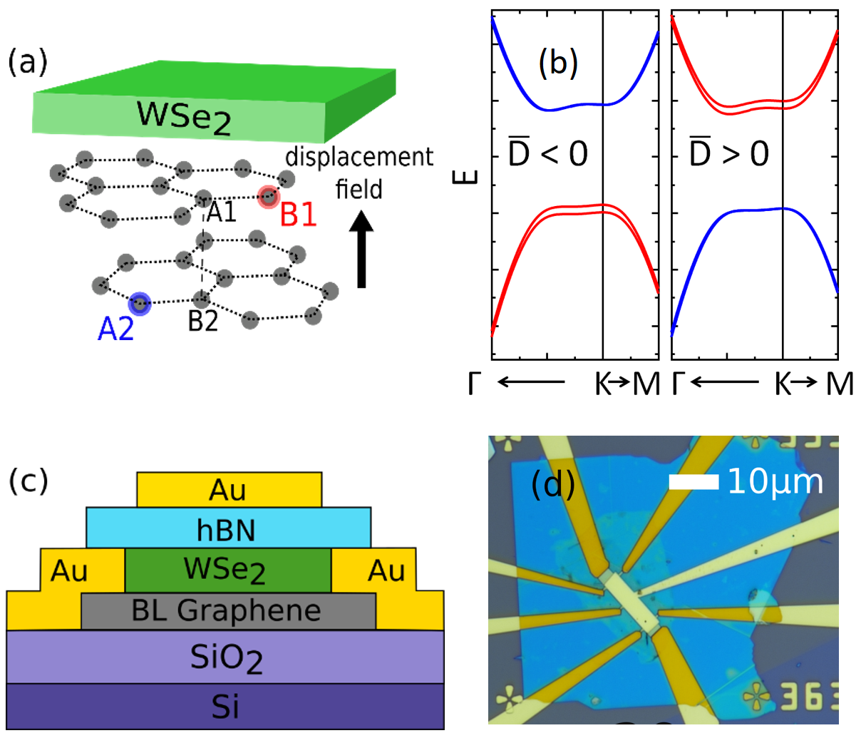
Spin-orbit coupling (SOC) is central to topological insulators [1, 2, 3, 4, 5] and spintronics, both very active fields of current research in condensed matter physics. To add flexibility in device functions, it is highly desirable to tune SOC by applying a gate voltage, as in the original proposal for a spin field effect transistor by Datta and Das [6]. Graphene is an excellent material for spintronics, as its intrinsic SOC is very low [7], leading to large spin lifetimes [8]. SOC can then be induced by proximity coupling to transition metal dichalcogenides [9, 10], leading to dramatic modification of spin transport [11, 12, 13, 14, 15, 16, 17], or weak antilocalization (WAL) in magnetotransport [18, 19, 20, 21, 22, 23, 24]. In addition, robust, spin-polarized edge channels were recently predicted for a graphene/WSe2 heterostructure [25]. Here, again, gate control of SOC would be strongly beneficial. In single layer graphene (SLG)/TMDC heterostructures, gate tunability of SOC is only quite modest [26, 21]. However, in a heterostructure of bilayer graphene (BLG) and a TMDC on one side only, strong gate tunability of SOC was recently predicted [27, 28]. The underlying mechanism is quite intuitive: At low carrier densities, an out-of-plane displacement field opens a gap in BLG, and leads to a selective population of one of the two layers only, with opposite trend for the valence band (VB) and conduction band (CB). More precisely, the occupancy of layers 1 and 2 is governed by the layer polarization [29, 28]:
| (1) |
Here, is the potential energy on layers 1 and 2, plus and minus sign correspond to layer 1 and 2, and for valence and conduction band, respectively. Layer 1 is closer to WSe2 (see Fig. 1 (a)), thus the charge carriers in it experience a much stronger proximity-induced SOC than the carriers in the other layer. Hence, the strength of induced SOC in BLG can be conveniently tuned by gate voltages. The behavior is opposite for electrons and holes due to the inversion of the bandstructure by the applied transverse electric field. The transition between high and low SOC strength is sharpest for low carrier densities, and softens considerably when going to higher densities.
A full density functional calculation [27] of the band structure of BLG/TMDC shows that, depending on the field polarity, spin splitting is predominantly found in either VB or CB (see Fig. 1 (b) for a corresponding tight-binding calculation). The out-of-plane field is composed of both built-in and gate-controlled fields. For details, we refer in particular to Fig. 4 of Ref. [27]. Recent charge transport and capacitance experiments confirmed the presence of an SOC gap, which depends on the gate voltage and carrier type [30, 31].
To confirm the implications of proximity-induced SOC on spin dynamics, WAL experiments are frequently employed [32, 18, 19, 20, 21, 22, 23, 24]. WAL is a phase-coherent effect, which is visible whenever the phase relaxation time is long enough. In BLG, without SOC, weak localization (WL, visible as a dip in magnetoconductance around ) is found [33, 34], while the observation of WAL (a peak in magnetoconductance around ) confirms the presence of SOC, as WAL does not appear in BLG without strong SOC due to the Berry phase of [35]. In the intuitive picture outlined above, one would therefore expect to observe a monotonic increase of the WAL feature when the electric field is tuned such that spin splitting increases. In the following, we present a detailed experimental and theoretical study of WAL in BLG/WSe2 showing that SOC is indeed strongly gate-tunable, as proposed recently, but the gate-dependence of WAL counterintuitively shows a non-monotonic dependence on . The experiments are confirmed by calculations of the spin relaxation rates using a model Hamiltonian of BLG with proximity-induced SOC on one layer only.
II Experiment
In total, we present experimental data taken from three samples, A, B and C. Data from A and B are shown in the main text, additional data from the lower quality sample C are shown in the Supplemental Material [36].
II.1 Sample fabrication
Heterostructures were fabricated by using a hot pickup process with a polycarbonate film on polydimethylsiloxane (PDMS) [37]. A cross-section of the device is shown schematically in Fig. 1(c). Bernal stacked bilayer graphene was picked up by exfoliated WSe2 with a thickness of a few tens of nanometers, and placed onto a standard p++-doped Si/SiO2 chip which functions as a back gate of the device. A Hall-bar structure was defined by electron-beam lithography (EBL) and reactive ion etching (RIE) with CHF3/O2 [38]. Then, EBL and a RIE process with SF6 were employed to selectively remove the WSe2 at the contact areas [39]. The uncovered graphene was then contacted by 0.5 nm Cr / 40 nm Au. These contacts showed higher reliability and lower contact resistance compared to commonly used edge contacts. Hexagonal boron nitride (hBN) was placed on top of this device to serve as an additional dielectric for the subsequently deposited Au top gate. In Fig. 1 (d) an optical microscope image of the finished sample A is depicted. With this dual gated device it is possible to independently tune charge carrier concentration and applied electric field [40, 41].
.
II.2 Characterization
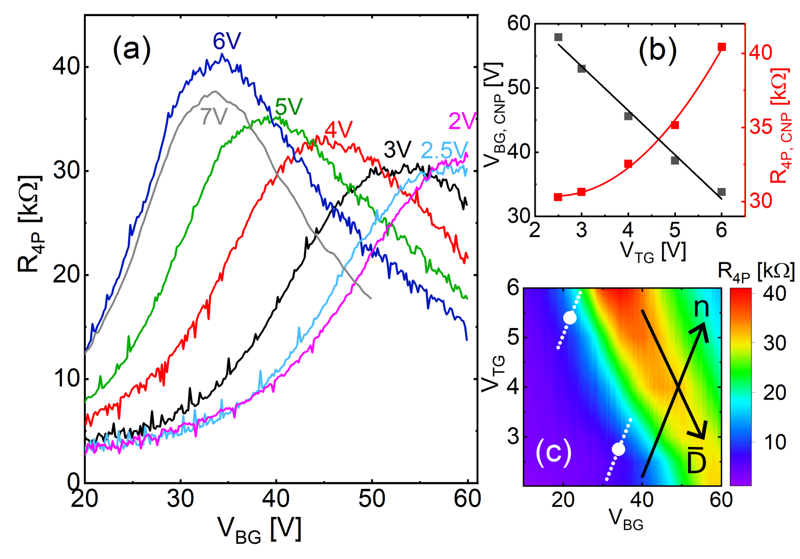
All measurements were performed at a temperature of K with an AC current of nA at a frequency of Hz. Figure 2 (a) shows the four-point resistance of sample A as a function of the back gate voltage for different top gate voltages. The corresponding gate map can be seen in Fig. 2 (c). The back gate voltage position and maximum resistivity at the charge neutrality point (CNP) shift by varying the applied top gate voltage. This is caused by the electric field induced bandgap in bilayer graphene and the shift of the Fermi level via the applied top and back gate voltages [41, 40]. The CNP position depends linearly on shown by the black squares in Fig. 2 (b). Further, the resistivity at the CNP shows a parabolic dependence on , shown in Fig. 2 (b) with red squares. The minimum of the parabolic fit corresponds to the top gate/back gate combination ( V, V), where the band gap in bilayer graphene vanishes, as both built-in electric fields and gate-controlled fields combine to a zero effective transverse electric field . From the combination of top and back gate capacitive coupling, we extract the required directions on the gate map to change either carrier density or displacement field , shown as arrows in Fig. 2 (c). Here, and are obtained in the following way [40]:
| (2) |
with
| (3) |
where and are the capacitive couplings of back and top gate dielectrics, respectively. The polarity of is positive for the electric field pointing from back gate to top gate, i.e., from BLG to TMDC.
The gate map depicted in Fig. 2 (c) is limited by the back gate range, as an applied voltage higher than 60 V might cause a breakdown of the back gate dielectric, destroying the sample. The CNP of the curve at a top gate voltage of 7 V in Fig. 2 (a) does not follow the parabolic behavior of the other CNPs. The reason for this is that at top gate voltages higher than 6 V the Fermi level in WSe2 is shifted into the conduction band and free electrons screen the top gate [27]. Therefore, the range of possible combinations of charge carrier densities and transverse electric fields was limited, and we could only study WAL in the hole regime of sample A.
The mobility on the hole-side of = 3000 cm2/Vs can be extracted from the curve at 2.5 V top gate voltage in Fig. 2(a) which shows the lowest CNP. This leads to a mean free path of nm for a charge carrier density of m-2.
II.3 Weak antilocalization of sample A
The physics of WAL was calculated by McCann and Fal’ko for graphene subject to SOC terms in the Hamiltonian, which conserve or break symmetry [32]. Those terms lead to the spin relaxation rates and , respectively, which can, in principle, be determined by fitting the experimental data to the McCann theory. For a full description of WAL in SLG and BLG, the graphene-specific scattering times (intervalley scattering time) and (which contains the intravalley scattering time by ) are included:
| (4) |
with , the digamma function, and the diffusion constant [22, 32, 42, 43]. In the last row, the plus sign is for SLG, and the minus sign for BLG [43].
Inspection of this equation shows that can be determined quite accurately, while the other scattering times are cross-dependent on one another in the fitting procedure. When WAL is observed (a peak in magnetoconductivity at T), SOC is certainly present. The absence of WAL, or presence of WL can be due to the lack of sizable SOC, or due to a long lifetime . The interpretation of experimental data is thus quite involved [32, 22]. Note that the above holds for BLG, where without SOC, WAL cannot be observed due to the Berry phase of [35]. In SLG, on the other hand, WAL can also be observed without SOC for certain combinations of elastic scattering times [44].
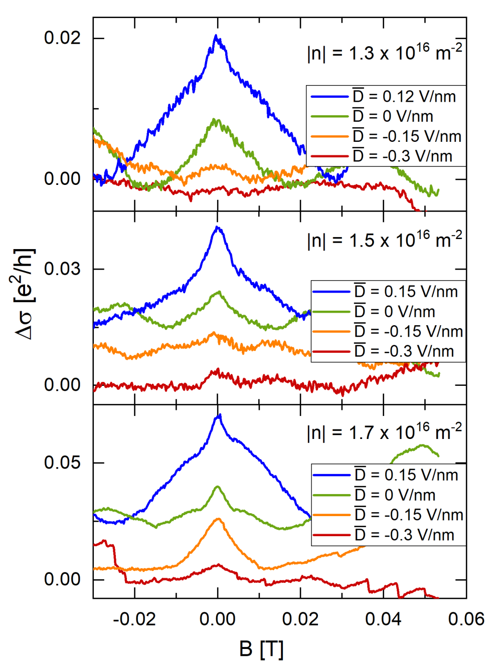
Figure 3 shows the dependence of the conductivity of sample A on an out-of plane magnetic field at different charge carrier concentrations and various displacement fields . As the scattering times and in Eq. 4 might depend on the carrier density, varying at fixed carrier density enables us to single out the effect of an electric field on SOC. The magnetoconductivity curves are averaged over 31 measurements at slightly different charge carrier concentrations and constant transverse electric field to suppress universal conductance fluctuations (UCF) [45, 46, 18]. A parabolic background fitted to reference measurements taken at K was subtracted. Here, for all curves a conductivity peak arises around T, stemming from WAL. We observe a strong gate-dependence of WAL, confirming the gate-tunability of SOC, but the trend in is opposite to what is expected: We find that in the hole regime, the WAL feature becomes more pronounced as increases, but overall spin splitting should decrease in this direction. We note that fitting the experimental data to Eq. 4 is ambiguous, as widely varying values for and lead to acceptable fitting results (see Supplemental Material [36] for ambiguity of fitting and also the suppression of WAL with increasing [47]). For SLG/TMDC, it was proposed [22] to fix the ratio of and to a value determined from spin precession experiments in spin valve devices [48], but this approach is bound to fail in BLG/TMDC, as we will show below.
III Theory of the gate dependence of WAL
To elucidate the counterintuitive gate dependence of WAL, we calculate the gate dependence of the spin relaxation times and using a model Hamiltonian describing BLG in one-sided contact to a TMDC layer. Those times are then inserted into Eq. 4, together with the remaining scattering times extracted from experiment.
III.1 Calculation of spin relaxation times
We calculate the spin relaxation following the procedure presented by Cummings et al. [11] for SLG/TMDC. Assuming the Dyakonov-Perel’-mechanism, symmetric and asymmetric rates are calculated by
| (5) |
where is the momentum relaxation time, and the squares of the spin precession frequencies around the spin-orbit fields in , , and directions are averaged along the Fermi contour. Note that those rates do not directly correspond to the spin relaxation times for spins oriented along the , , or -axis, as would be measured in a spin transport experiment [48, 49]. We obtain the precession frequencies for electrons and holes using the model Hamiltonian described in the Appendix. The strength of valley-Zeeman and Rashba SOC in the graphene layer close to WSe2 is given by and , respectively, while in the other graphene layer, SOC is set to zero. From the eight bands, we only consider the four innermost spin-resolved valence and conduction bands, which are composed predominantly from states residing on B1 and A2 (see Fig. 1 (a)). can be determined self-consistently from [50] (see Supplemental Material [36]). Using an effective mass of times the free electron mass [51] and typical densities from our experiment, this results approximately in a relation with the units in eV, and V/nm, respectively, which we use for simplicity in the following.
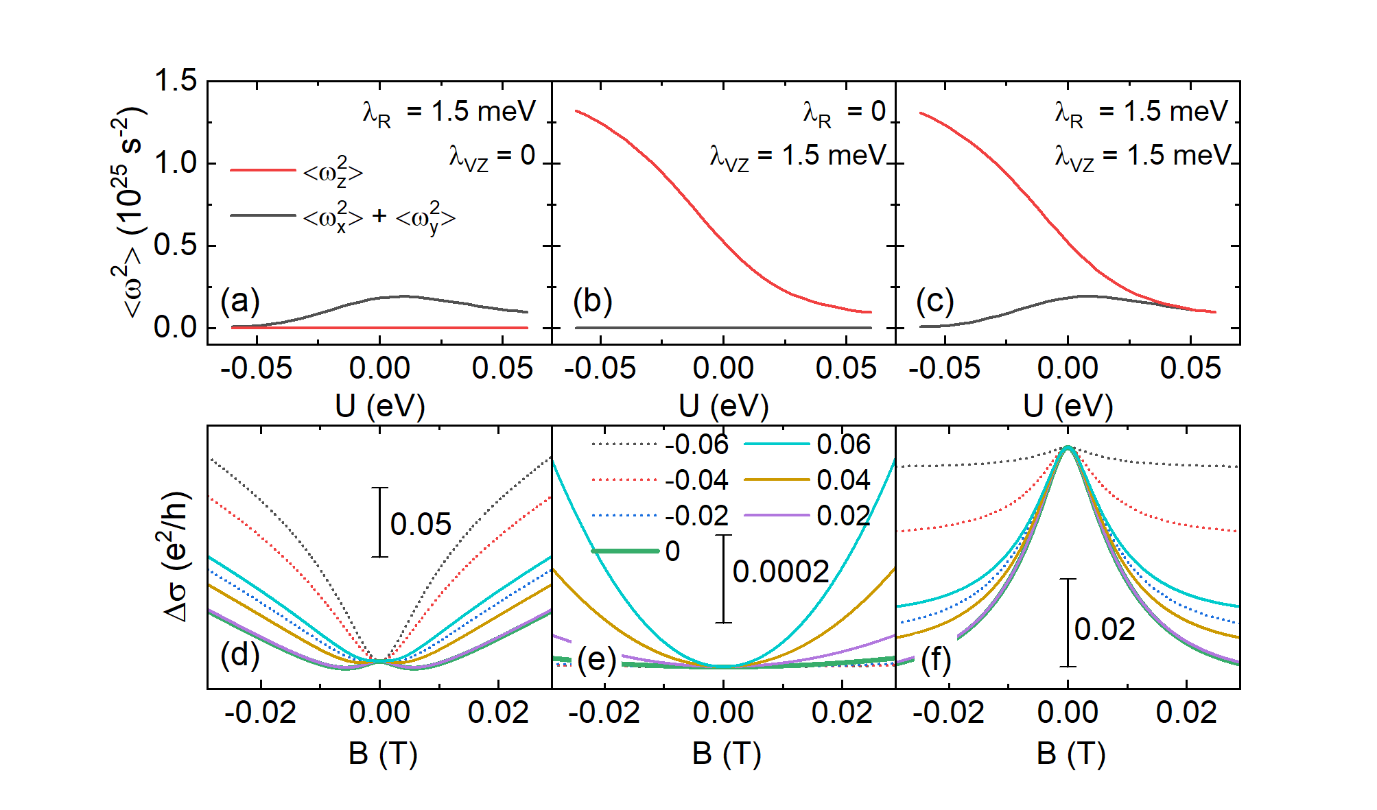
The resulting gate dependence of the squared precession frequencies around and is plotted in Fig. 4(a) to (c) for several combinations of and and a carrier concentration of m-2 of holes. We find that both quantities show a strong gate dependence, but with an opposite trend. While decreases with , thus following the expected trend, the precession around the and axes shows a maximum at eV. As the latter frequency enters into the asymmetric scattering rate , which is essential to observing WAL, and not WL, this gives us a first clue to understanding the peculiar gate dependence of WAL. We also note that the ratio varies strongly with at a given density . Furthermore, as expected, setting the valley-Zeeman term to zero suppresses precession around the -axis (panel (a)), while setting the Rashba term to zero eliminates precession around the and axis (panel (b)).
III.2 Gate dependence of WAL
The precession frequencies calculated in the previous section can now be translated into WAL curves. To simulate WAL in graphene, we take typical scattering times well suited to transport results from sample A: ps is extracted from the width of the WAL feature at K and is comparable to the phase coherence time obtained by taking the autocorrelation of UCFs (see Supplemental Material [36] and also [52, 53, 54]). m2/s and fs are obtained from typical mobilities of our samples, ps and ps are taken from reference samples where WSe2 was replaced by hexagonal boron nitride on top of BLG. Note that enters into through Eq. 5. The exact values of and determine the curve shape, overall effect height, and bending of the curves at higher fields. Due to the large number of free parameters in Eq. 4, these parameters cannot be determined unambiguously. However, the curves shown in Fig. 4 reflect the trend of the gate dependence of WAL over a wide range of parameters. We observe that when only Rashba SOC is present (panel (d)), a transition from WL to WAL is found when increasing from negative values to eV, and the trend eventually reverses for eV. The transition from WL to WAL is still obtained when , and (not shown). When and only , WAL is never found. The overall effect strength is tiny (note the scale bar in panel (e)) and WL strength can be slightly tuned with . When both and are non-zero, WAL is observed, and its strength can be tuned with , but with a non-monotonic behavior. In our model, the highest WAL peak is observed for , but this can be slightly modified when the graphene layer away from TMDC also bears a small SOC, as for intrinsic graphene. In the model presented in the Appendix, this small contribution is neglected.
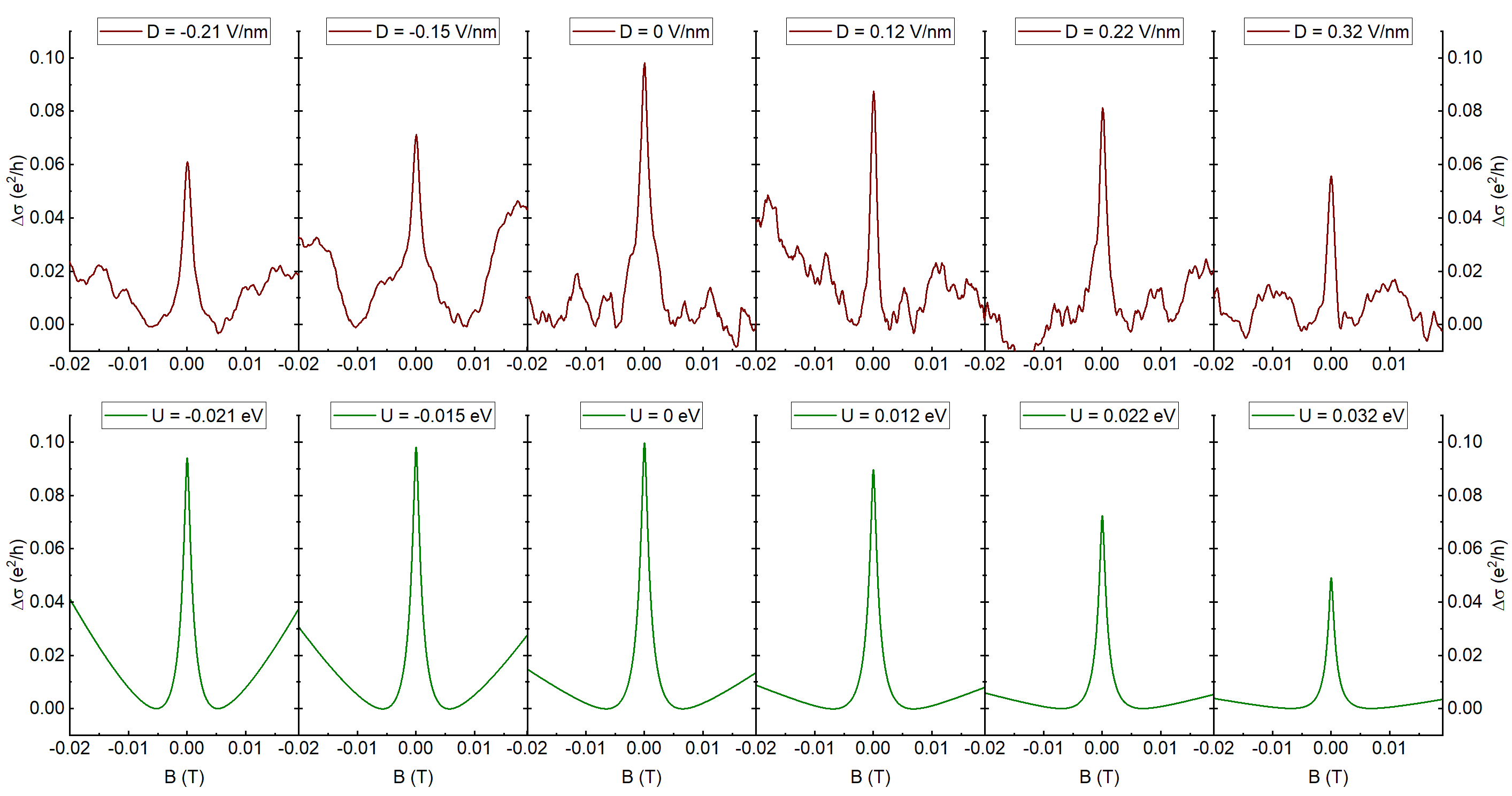
Finally, we compare experimental data obtained from sample B, in the electron regime, with the results of our model (see Fig. 5). As in sample B the charge neutrality point is found at smaller gate voltages, we can access both the electron and the hole regime. In the electron regime, could be varied over a broader range so as to explore the behaviour on both sides of . For the modeling, we used ps, fs, fs, ps, m2/s, m-2 (from transport characterization and reference samples) and meV, meV to obtain a visual match. The similarity is quite striking. Both experiment and theory show the most pronounced WAL feature at zero out of plane electric field with a drop in visibility on both sides [55]. This behavior is at odds with the simpler expectation gained from Eq. 1, but is the result of the intricate dependence of Eq. 4 on two different, SOC-based relaxation rates. Mainly, as WAL in graphene with SOC can only be observed if a sizable rate is present, its non-monotonic dependence on the out-of-plane electric field directly determines the non-monotonic evolution of WAL with the gate voltage. The values for the SOC strength and are in good agreement with results from density functional theory. Moreover, using the same and , we can also achieve good agreement for WAL data in the hole regime, and the electron regime at a different density (see Supplemental Material [36]).
IV Discussion and Conclusion
Our results show that, while SOC is indeed strongly gate tunable in BLG/TMDC heterostructures, the interpretation of WAL experiments is not straightforward. Unlike the SLG/TMDC case, or the TMDC/BLG/TMDC heterostructure (which we both checked in our formalism using appropriate model Hamiltonians), the spin splittings projected to the , and -directions are strongly density and gate dependent. In particular, the average along the Fermi contour is non-monotonic in the out-of-plane electric field, and enters into the scattering rate . The latter is crucial for observing WAL in graphene with SOC. When only is relevant, one still observes WL with a reduced amplitude, even though SOC is present [32]. In the simplest case, when only proximity induced SOC in one graphene layer is considered, the maximum visibility of WAL is present at precisely (corresponding to in experiment). On the other hand, setting SOC in the other graphene layer to small values, as in the pristine graphene case, can shift this maximum slightly away from , but the general trend remains. Lastly, we briefly comment on a recent experimental demonstration of gate-tunable SOC in a similiar heterostructure by Tiwari et al. [56]. Their results are not in line with the experimental and theoretical data in this study. We note, however, that in their article there is an inconsistency regarding the definition of the field direction between the formula in the text and the corresponding illustration.
In conclusion, we demonstrate a clear gate tunability of WAL in bilayer graphene, in proximity to WSe2 on one side, which can be fully explained by calculations of the SOC induced spin relaxation. The fact that the visibility of WAL does not follow the gate-induced electric field monotonically, as might be expected at first sight, is accounted for by the intricate dependence of WAL in graphene on two SOC related scattering rates, and their non-monotonic dependence on the gate voltages.
Acknowledgements.
K.W. and T.T. acknowledge support from the Elemental Strategy Initiative conducted by the MEXT, Japan, Grant Number JPMXP0112101001, JSPS KAKENHI Grant Number JP20H00354 and the CREST(JPMJCR15F3), JST. This work was funded by the Deutsche Forschungsgemeinschaft (DFG, German Research Foundation) through SFB 1277 (project-id 314695032, subprojects A09, B07), GRK 1570, SFB 689 and ER 612/2 (project id. 426094608). We thank T. Frank for fruitful discussions. We are particularly grateful to C. Stampfer and E. Icking for enlightening discussions of the sign of .Appendix A Hamiltonian
The electronic band structure of bilayer graphene in proximity to WSe2 is obtained from the full Hamiltonian in the spirit of Refs. [50, 57]. Its orbital part counts the relevant nearest intra- and inter-layer hoppings called conventionally as eV, eV, eV and eV including also the dimer energy-shift meV. The above values are taken from Ref. [57]. The effect of the transverse displacement field on the electronic states in the top and bottom layers is captured by the on-site potential energy . In the experiment the built-in dipole field of the bilayer due to the WSe2 is counteracted by the external gates and from that reference configuration one measures displacement field and hence also the potential energy . For those reasons the model Hamiltonian does not involve any dipole fields. The full orbital Hamiltonian in the Bloch basis based on atomic orbitals , , , , , , , , for their atomic positions see Fig. 1(a), is given as:
| (6) |
In the above expression is measured from the point, and
| (7) |
is the tight-binding structural function including the lattice vectors and the graphene lattice constant nm.
To model the spin-orbit part we assume only the spin-orbit couplings in the proximitized top layer, namely, the next-nearest neighbor spin conserving VZ-term , and the nearest neighbor spin flipping Rashba coupling . These are assumed to be enhanced due to the proximity of WSe2, and close to the Dirac points they are primarily responsible for splitting of the electronic bands. The corresponding given in the same basis , , , , , , , is as follows:
| (8) |
and the corresponding tight-binding functions read:
| (9) | ||||
| (10) | ||||
| (11) |
The model Hamiltonian with the parameters and is used to calculate the spin-resolved bands and the spin relaxation rates. The layer dependent energy term can be determined self-consistently from [50] (see Supplemental Material [36]). Using an effective mass of times the free electron mass [51], for simplicity we approximate by a relation with the units in eV, and V/nm, respectively.
References
- Kane and Mele [2005a] C. L. Kane and E. J. Mele, Phys. Rev. Lett. 95, 226801 (2005a).
- Kane and Mele [2005b] C. L. Kane and E. J. Mele, Phys. Rev. Lett. 95, 146802 (2005b).
- Bernevig and Zhang [2006] B. A. Bernevig and S.-C. Zhang, Phys. Rev. Lett. 96, 106802 (2006).
- Bernevig et al. [2006] B. A. Bernevig, T. L. Hughes, and S.-C. Zhang, Science 314, 1757 (2006).
- König et al. [2007] M. König, S. Wiedmann, C. Brune, A. Roth, H. Buhmann, L. W. Molenkamp, X.-L. Qi, and S.-C. Zhang, Science 318, 766 (2007).
- Datta and Das [1990] S. Datta and B. Das, Appl. Phys. Lett. 56, 665 (1990).
- Gmitra et al. [2009] M. Gmitra, S. Konschuh, C. Ertler, C. Ambrosch-Draxl, and J. Fabian, Phys. Rev. B 80, 235431 (2009).
- Han et al. [2014] W. Han, R. K. Kawakami, M. Gmitra, and J. Fabian, Nat Nano 9, 794 (2014).
- Kaloni et al. [2014] T. P. Kaloni, L. Kou, T. Frauenheim, and U. Schwingenschlögl, Applied Physics Letters 105, 233112 (2014).
- Gmitra et al. [2016] M. Gmitra, D. Kochan, P. Högl, and J. Fabian, Phys. Rev. B 93, 155104 (2016).
- Cummings et al. [2017] A. W. Cummings, J. H. Garcia, J. Fabian, and S. Roche, Phys. Rev. Lett. 119, 206601 (2017).
- Ghiasi et al. [2017] T. S. Ghiasi, J. Ingla-Aynés, A. A. Kaverzin, and B. J. van Wees, Nano Letters 17, 7528 (2017).
- Benítez et al. [2017] L. A. Benítez, J. F. Sierra, W. Savero Torres, A. Arrighi, F. Bonell, M. V. Costache, and S. O. Valenzuela, Nature Physics 14, 303 (2017).
- Garcia et al. [2017] J. H. Garcia, A. W. Cummings, and S. Roche, Nano Letters 17, 5078 (2017).
- Ghiasi et al. [2019] T. S. Ghiasi, A. A. Kaverzin, P. J. Blah, and B. J. van Wees, Nano Lett. 19, 5959 (2019).
- Safeer et al. [2019] C. K. Safeer, J. Ingla-Aynés, F. Herling, J. H. Garcia, M. Vila, N. Ontoso, M. R. Calvo, S. Roche, L. E. Hueso, and F. Casanova, Nano Letters 19, 1074 (2019).
- Benítez et al. [2020] L. A. Benítez, W. Savero Torres, J. F. Sierra, M. Timmermans, J. H. Garcia, S. Roche, M. V. Costache, and S. O. Valenzuela, Nature Materials 19, 170 (2020).
- Wang et al. [2015] Z. Wang, D.-K. Ki, H. Chen, H. Berger, A. H. MacDonald, and A. F. Morpurgo, Nat Commun 6, (2015).
- Wang et al. [2016] Z. Wang, D.-K. Ki, J. Y. Khoo, D. Mauro, H. Berger, L. S. Levitov, and A. F. Morpurgo, Phys. Rev. X 6, 041020 (2016).
- Yang et al. [2016] B. Yang, M.-F. Tu, J. Kim, Y. Wu, H. Wang, J. Alicea, R. Wu, M. Bockrath, and J. Shi, 2D Materials 3, 031012 (2016).
- Völkl et al. [2017] T. Völkl, T. Rockinger, M. Drienovsky, K. Watanabe, T. Taniguchi, D. Weiss, and J. Eroms, Phys. Rev. B 96, 125405 (2017).
- Zihlmann et al. [2018] S. Zihlmann, A. W. Cummings, J. H. Garcia, M. Kedves, K. Watanabe, T. Taniguchi, C. Schönenberger, and P. Makk, Phys. Rev. B 97, 075434 (2018).
- Wakamura et al. [2018] T. Wakamura, F. Reale, P. Palczynski, S. Guéron, C. Mattevi, and H. Bouchiat, Phys. Rev. Lett. 120, 106802 (2018).
- Afzal et al. [2018] A. M. Afzal, M. F. Khan, G. Nazir, G. Dastgeer, S. Aftab, I. Akhtar, Y. Seo, and J. Eom, Scientific Reports 8, 3412 (2018).
- Frank et al. [2018] T. Frank, P. Högl, M. Gmitra, D. Kochan, and J. Fabian, Phys. Rev. Lett. 120, 156402 (2018).
- Gmitra and Fabian [2015] M. Gmitra and J. Fabian, Phys. Rev. B 92, 155403 (2015).
- Gmitra and Fabian [2017] M. Gmitra and J. Fabian, Phys. Rev. Lett. 119, 146401 (2017).
- Khoo et al. [2017] J. Y. Khoo, A. F. Morpurgo, and L. Levitov, Nano Letters 17, 7003 (2017).
- Young and Levitov [2011] A. F. Young and L. S. Levitov, Phys. Rev. B 84, 085441 (2011).
- Island et al. [2019] J. O. Island, X. Cui, C. Lewandowski, J. Y. Khoo, E. M. Spanton, H. Zhou, D. Rhodes, J. C. Hone, T. Taniguchi, K. Watanabe, L. S. Levitov, M. P. Zaletel, and A. F. Young, Nature 571, 85 (2019).
- Wang et al. [2019] D. Wang, S. Che, G. Cao, R. Lyu, K. Watanabe, T. Taniguchi, C. N. Lau, and M. Bockrath, Nano Letters 19, 7028 (2019).
- McCann and Fal’ko [2012] E. McCann and V. I. Fal’ko, Phys. Rev. Lett. 108, 166606 (2012).
- Bergmann [1983] G. Bergmann, Phys. Rev. B 28, 2914 (1983).
- McCann et al. [2006] E. McCann, K. Kechedzhi, V. I. Fal’ko, H. Suzuura, T. Ando, and B. L. Altshuler, Phys. Rev. Lett. 97, 146805 (2006).
- Kechedzhi et al. [2007] K. Kechedzhi, E. McCann, V. I. Fal’ko, H. Suzuura, T. Ando, and B. L. Altshuler, The European Physical Journal Special Topics 148, 39 (2007).
- [36] See Supplemental Material at [URL will be inserted by the production group] for self-consistent calculation of the band gap, additional experimental data, transport parameters, and data on universal conductance fluctuations.
- Pizzocchero et al. [2016] F. Pizzocchero, L. Gammelgaard, B. S. Jessen, J. M. Caridad, L. Wang, J. Hone, P. Bøggild, and T. J. Booth, Nature Communications 7, 11894 (2016).
- Wang et al. [2013] L. Wang, I. Meric, P. Y. Huang, Q. Gao, Y. Gao, H. Tran, T. Taniguchi, K. Watanabe, L. M. Campos, D. A. Muller, J. Guo, P. Kim, J. Hone, K. L. Shepard, and C. R. Dean, Science 342, 614 (2013).
- Son et al. [2018] J. Son, J. Kwon, S. Kim, Y. Lv, J. Yu, J.-Y. Lee, H. Ryu, K. Watanabe, T. Taniguchi, R. Garrido-Menacho, N. Mason, E. Ertekin, P. Y. Huang, G.-H. Lee, and A. M. van der Zande, Nature Communications 9, 3988 (2018).
- Zhang et al. [2009] Y. Zhang, T.-T. Tang, C. Girit, Z. Hao, M. C. Martin, A. Zettl, M. F. Crommie, Y. R. Shen, and F. Wang, Nature 459, 820 (2009).
- Oostinga et al. [2008] J. B. Oostinga, H. B. Heersche, X. Liu, A. F. Morpurgo, and L. M. K. Vandersypen, Nat Mater 7, 151 (2008).
- Ilič et al. [2019] S. Ilič, J. S. Meyer, and M. Houzet, Phys. Rev. B 99, 205407 (2019).
- McCann and Fal’ko [2021] E. McCann and V. Fal’ko, personal communication (2021).
- Tikhonenko et al. [2009] F. V. Tikhonenko, A. A. Kozikov, A. K. Savchenko, and R. V. Gorbachev, Phys. Rev. Lett. 103, 226801 (2009).
- Gorbachev et al. [2007] R. V. Gorbachev, F. V. Tikhonenko, A. S. Mayorov, D. W. Horsell, and A. K. Savchenko, Phys. Rev. Lett. 98, 176805 (2007).
- Tikhonenko et al. [2008] F. V. Tikhonenko, D. W. Horsell, R. V. Gorbachev, and A. K. Savchenko, Phys. Rev. Lett. 100, 056802 (2008).
- Narozhny et al. [2002] B. N. Narozhny, G. Zala, and I. L. Aleiner, Phys. Rev. B 65, 180202 (2002).
- Omar et al. [2019] S. Omar, B. N. Madhushankar, and B. J. van Wees, Phys. Rev. B 100, 155415 (2019).
- Note [1] In a Hanle experiment, typically the relaxation rates for spins oriented in or out of the graphene plane are measured, while here the distinction is made by the underlying SOC mechanisms.
- McCann and Koshino [2013] E. McCann and M. Koshino, Reports on Progress in Physics 76, 056503 (2013).
- Li et al. [2016] J. Li, L. Z. Tan, K. Zou, A. A. Stabile, D. J. Seiwell, K. Watanabe, T. Taniguchi, S. G. Louie, and J. Zhu, Phys. Rev. B 94, 161406 (2016).
- Pezzini et al. [2012] S. Pezzini, C. Cobaleda, E. Diez, and V. Bellani, Phys. Rev. B 85, 165451 (2012).
- Lundeberg et al. [2012] M. B. Lundeberg, J. Renard, and J. A. Folk, Phys. Rev. B 86, 205413 (2012).
- Lundeberg et al. [2013] M. B. Lundeberg, R. Yang, J. Renard, and J. A. Folk, Phys. Rev. Lett. 110, 156601 (2013).
- Note [2] At negative fields the drop in the simulation is not as pronounced as in the experiment. This can be improved with a shorter, but unrealistic, or by including some SOC on the graphene layer far from the TMDC.
- Tiwari et al. [2021] P. Tiwari, S. K. Srivastav, and A. Bid, Phys. Rev. Lett. 126, 096801 (2021).
- Konschuh et al. [2012] S. Konschuh, M. Gmitra, D. Kochan, and J. Fabian, Phys. Rev. B 85, 115423 (2012).