Physical Mechanism behind the Hysteresis-free Negative Capacitance Effect in Metal-Ferroelectric-Insulator-Metal Capacitors with Dielectric Leakage and Interfacial Trapped Charges
Abstract
The negative capacitance (NC) stabilization of a ferroelectric (FE) material can potentially provide an alternative way to further reduce the power consumption in ultra-scaled devices and thus has been of great interest in technology and science in the past decade. In this article, we present a physical picture for a better understanding of the hysteresis-free charge boost effect observed experimentally in metal-ferroelectric-insulator-metal (MFIM) capacitors. By introducing the dielectric (DE) leakage and interfacial trapped charges, our simulations of the hysteresis loops are in a strong agreement with the experimental measurements, suggesting the existence of an interfacial oxide layer at the FE-metal interface in metal-ferroelectric-metal (MFM) capacitors. Based on the pulse switching measurements, we find that the charge enhancement and hysteresis are dominated by the FE domain viscosity and DE leakage, respectively. Our simulation results show that the underlying mechanisms for the observed hysteresis-free charge enhancement in MFIM may be physically different from the alleged NC stabilization and capacitance matching. Moreover, the link between Merz’s law and the phenomenological kinetic coefficient is discussed, and the possible cause of the residual charges observed after pulse switching is explained by the trapped charge dynamics at the FE-DE interface. The physical interpretation presented in this work can provide important insights into the NC effect in MFIM capacitors and future studies of low-power logic devices.
pacs:
Valid PACS appear hereI Introduction
As the relentless pursuit of device miniaturization goes into the nanometer regime, Moore’s law has gradually come to a bottleneck due to the fact that the power dissipation in microchips becomes a more and more challenging concern Moore (1998); Kim et al. (2003). Recently, a stack structure consisting of an FE layer and a DE layer was proposed to achieve voltage amplification in a DE layer Salahuddin and Datta (2008). The physical concept behind this approach is that the metastable negative capacitance (NC) state arising from the double-well energy profile of the FE can be stabilized by the DE layer in terms of the total free energy of the system. Such a proposal may provide a potential way to significantly improve the subthreshold swing of conventional complementary metal-oxide-semiconductor (CMOS) transistors at room temperature Chang et al. (2017); Hsu et al. (2018).
Ferroelectrics are materials that exhibit the properties: (i) the electric polarization can be reversed by an externally applied voltage and (ii) the remanent polarization remains nonvolatile under zero bias. These unique properties have made ferroelectrics promising materials for voltage-controlled nonvolatile memory devices Ni et al. (2018a, b). In the past decade since the proposal of using NC for low-power logic devices, FE-based capacitors, including MFM, MFIM and metal-ferroelectric-metal-insulator-metal (MFMIM), have been intensively investigated experimentally and theoretically in search of the evidence for the transient and steady-state NC effects Khan et al. (2014); Gao et al. (2014); Appleby et al. (2014); Kim et al. (2016a); Hoffmann et al. (2016); Chang et al. (2018); Hoffmann et al. (2018, 2019); Kim et al. (2019); Hsu et al. (2020). In particular, recently discovered doped hafnium oxides are widely used as the FE layer due to the high scalability and CMOS process compatibility Böscke et al. (2011); Müller et al. (2012); Sharma et al. (2017).
With an MFM capacitor connected in series with a large resistor, the transient NC behaviors have been observed in various FE materials, including perovskite \chPb(Zr_0.2Ti_0.8)O3 and various doped hafnium oxides Khan et al. (2014); Hoffmann et al. (2016); Kobayashi et al. (2016). The physical origin of the observed transient NC lies in the mismatch between the switching rates of free charges and bound charges (FE polarization) in the resistor-capacitor circuit Chang et al. (2018). To further seek the evidence of static NC stabilization, FE-DE stacks are the key devices to be investigated according to the NC theory. Among MFIM, MFMIM and FE-DE superlattices, MFIM capacitors are of great importance because of the structure similarity to the ferroelectric field effect transistors (FeFETs). For MFIM stacks, it is unlikely to directly measure the internal DE voltage amplification, which was theoretically proposed to be achieved by the steady-state NC stabilization. Therefore, a considerable amount of experimental efforts have been focused on the evidence of capacitance enhancement in an MFIM capacitor compared to the associated standalone DE capacitor Alam et al. (2019). Such a capacitance enhancement is referred to as the charge boost effect.
In the recent research progress, it was experimentally observed that the charge boost effect and hysteresis-free static “S-shaped curve” could be achieved in MFIM with short pulse measurements Hoffmann et al. (2018, 2019). On one hand, the charge boost may indicate that the MFIM capacitor has a larger capacitance than the associated DE capacitor, which was allegedly caused by the NC stabilization. On the other hand, the observed hysteresis-free FE switching (S-curve), which is predicted by the Landau phenomenological formalism, is a required characteristic for the logic applications. However, the physical mechanisms for these observations are still not clear. For example, Liu et al. have recently proposed an alternative perspective on such experimental observations Liu et al. (2020). Therefore, it is of great importance to further explore the underlying physical mechanisms for such prospective experimental evidence of NC stabilization.
In this paper, we establish a physical model for MFM and MFIM capacitors by introducing the inevitable DE leakage and trapped charges at the FE-DE interface. We show that the experimentally measured hysteresis loop of MFM capacitors can be well described by the Landau formalism with the proposed physical mechanisms included. The charge boost and hysteresis behaviors observed in the pulse measurements are found to be directly influenced by the FE intrinsic domain viscosity and DE leakage, respectively. The kinetic coefficients extracted from the charge responses are found to be linked to the well-known Merz’s law Merz (1956) in the NC region. Our simulation results suggest that the experimentally observed hysteresis-free capacitance enhancement of MFIM may be caused not by the NC stabilization and capacitance matching but by the material properties of the heterostructure. Furthermore, the possible cause of the experimentally observed residual charges may be explained by the trapped charges existing at the FE-DE interface.
This paper is organized as follows. In Sec. II, the theoretical approach is presented to describe the switching characteristics of MFM and MFIM capacitors, with the DE leakage and trapped charge mechanisms included. In Sec. III, based on the physical model, the FE material parameters can be well extracted using the hysteresis measurements. More importantly, the experimentally observed charge boost and hysteresis-free static S-curve are well captured, and a clear physical picture for such phenomena is provided and discussed in detail. In Sec. IV, we conclude this work by highlighting the underlying mechanisms for experimental observations.
II Theoretical Formalism
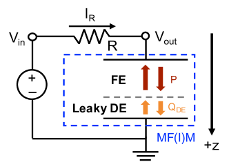
To describe the electrical properties of MFIM bilayer stacks measured in the experiments, Kirchhoff’s law is applied for the schematic circuit diagram shown in Fig. 1. The total current flowing through the series resistor is thus expressed as
| (1) |
where is the free charge density, is the series resistance and is the capacitor area. In addition, the following conditions have to be satisfied by assuming the electric displacement field is continuous at material boundaries:
| (2) |
where represents the DE leakage current, and and are the displacement current of the FE and the DE layers, respectively. Instead of the conventional DC leakage current, here describes the transient DE leakage due to the voltage across the DE layer, as will be detailed later.
In the FE layer, the displacement charge density can be written as
| (3) |
where is the vacuum dielectric constant, is the background dielectric constant of the FE material Tagantsev (2008), is the electric field across the FE oxide, and is the average FE polarization. The dynamics of is governed by the Landau-Khalatnikov (LK) equation,
| (4) |
where are thermodynamic expansion coefficients for the bulk FE free energy, and is the kinetic coefficient, which is inversely proportional to domain viscosity Landau (1937); Ginzburg (1945); Devonshire (1949); Hsu et al. (2018); Chang et al. (2018). Note that in this work, the free charge density is equal to the FE displacement charge density with the assumption that the leakage of an FE thin film is negligible Hoffmann et al. (2016).
It was experimentally reported that the trapped charges may exist at the FE-DE interface through the DE leakage, which plays an important role in the electrical properties and DE breakdown of MFIM capacitors Si et al. (2019). In this regard, we introduce DE leakage and interfacial trapped charges into the MFM and MFIM systems. For simplicity, the DE leakage for is approximated using field-assisted tunneling mechanism according to the experiments on ultrathin \chAl2O3 (AO) dielectrics Lin et al. (2005), where is the voltage across the DE layer and is the cutoff voltage below which the leakage current is negligible. is set to in this work. The leakage current when is above is therefore given by
| (5) |
where and are physical parameters related to the system band structures, is the electric field across the DE oxide, and a sign function is used for the current direction.
To extract the DE charge density accumulated at the DE-metal interface, we integrate the displacement current through the DE layer with respect to time:
| (6) |
where is the DE charges before switching. Note that is an initial condition in this framework and may vary from sample to sample depending on the experimental conditions.
At the FD-DE interface, the charge neutrality condition has to be satisfied due to the displacement field continuity in the normal direction. Therefore, the interfacial trapped charge can be obtained with the expression given by
| (7) |
where is the DE charge at the FE-DE interface.
III Results and Discussion
Based on the physical model described in Sec. II, we study the transient charge responses of MFM and MFIM capacitors, including hysteresis loops and pulse switching dynamics. The underlying physics behind the recent experimental observations is discussed in detail. For convenience, the theoretical model is implemented in a circuit-compatible manner so that all the dynamic simulations can be performed accurately and self-consistently in the SPICE simulator. The detailed implementation can be found in Hsu et al. (2020).
| Parameter | Value |
|---|---|
| Area | Hoffmann et al. (2018) |
| FE thickness | Hoffmann et al. (2018) |
| (m/F) | |
| 10 | |
| EOT | 0.1 |
| Frequency | 10 Hoffmann et al. (2018) |
| Pulse amplitude | 3.5 Hoffmann et al. (2018) |
III.1 MFM Capacitors
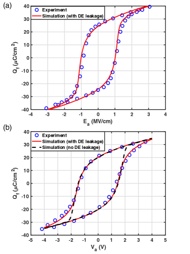
The MFIM stack structure of interest is TiN/\chHf_0.5Zr_0.5O2/\chAl2O3/TiN capacitors, where Zr-doped hafnium oxides (HZO) are a widely used FE material in the recent experimental measurements Kobayashi et al. (2016); Ni et al. (2018a); Hoffmann et al. (2018, 2019); Kim et al. (2019). Before we study the MFIM capacitors, we first extract the FE parameters by simulating the hysteresis loops of \chTiN/HZO/\chTiN MFM capacitors based on the conventional polarization-voltage (P-V) measurements. As suggested by the experiments Pešić et al. (2016); Kim et al. (2016b); Chouprik et al. (2019); Goh et al. (2020), an interfacial oxide layer is likely to form between the FE layer and the metal contacts during the fabrication process of MFM capacitors. In this regard, an ultrathin DE layer is introduced at the FE-metal interface of an MFM capacitor. Note that the depolarization, which is caused by the finite screening effect of the metal contacts, manifests itself with the interfacial oxide layer Lomenzo et al. (2020). Based on the P-V measurement in Ref. Hoffmann et al. (2018), the equivalent oxide thickness (EOT) of the interfacial oxide layer is found to be around given that the dielectric constant of \chSiO2 () is . The corresponding interfacial capacitance , which is consistent with the reported value for the FE/\chTiN interface Lomenzo et al. (2020). The physical thickness of the interfacial oxide layer can be estimated to be given the relative permittivity of for the tetragonal and orthorhombic phase in \chHfO2 and \chZrO2 Lomenzo et al. (2020). Fig. 2(a) shows the simulated hysteresis loop of an MFM capacitor based on the experimental P-V measurement in Ref. Hoffmann et al. (2018). To further confirm the effect of an oxide layer between the FE and the metal contact, we simulate the hysteresis loop of an MFM capacitor from another measurement Ni et al. (2018a), as shown in Fig. 2(b). The simulation without considering the interfacial oxide layer is also plotted for comparison. Our simulations indicate that the oxide layer at the FE-metal interface may be one of the important factors that could influence the hysteresis shape of MFM. The parameters extracted based on the experimental P-V measurement in Ref. Hoffmann et al. (2018) are summarized in Table 1. The FE properties of HZO are used for the study of MFIM capacitors.
III.2 MFIM Capacitors
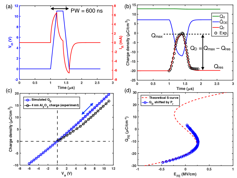
To study the TiN/HZO/AO/TiN capacitor, we apply the parameters obtained from the preceding section for HZO. Based on the experimental setup in Ref. Hoffmann et al. (2018), ascending and descending pulse trains with a pulse width (PW) were applied to the MFIM capacitor with HZO and AO. One of the voltage pulses and the total current flowing through the external resistor are shown in Fig. 3(a). Fig. 3(b) shows the corresponding transient free charge responses from the simulation. In the steady state before the pulse voltage is applied, the FE layer is in the negative remanent polarization state, as suggested in Ref. Hoffmann et al. (2018). To compensate the FE charge density, there must be the same amount of charges with opposite signs at the FE-DE interface. However, a dielectric material like AO cannot support a charge density as large as around for such a long period of time without breakdown Lin et al. (2005); Si et al. (2019). Therefore, here the initial DE charge is assumed to be reported in Ref. Si et al. (2019), and the rest of the compensating charges are from the interfacial trapped charge Si et al. (2019). Such a large amount of trapped charges are likely to be introduced through the DE leakage to the FE-DE interface during the wake-up process after the fabrication. At a large pulse amplitude, a large amount of negative DE charges accumulated at the FE-DE interface indicate that most of the applied voltage is across the DE layer in this stack system. Thus, in such pulse measurements, the FE polarization is barely switched even if a large voltage is applied. Similar to the experiments, the release charge is defined as the difference between the maximum charge and the residual charge at a given pulse amplitude ; that is, . At a fixed kinetic coefficient , it is found that of MFIM is enhanced without hysteresis compared to the measured charges on the associated standalone AO capacitor, as shown in Fig. 3(c). From the simulation, the electric field across the FE oxide, , can be directly obtained, and the theoretical static curve is derived from Eq. (4) in the steady state:
| (8) |
Fig. 3(d) shows that an S-curve with negligible hysteresis can be achieved with the DE leakage parameter . For the static curve, is shifted by , which is the initial reference point and was reported as around Hoffmann et al. (2018). Note that the S-curve obtained from the simulation does not go through the origin because for the FE response has not been calibrated dynamically based on the polarization charge responses.
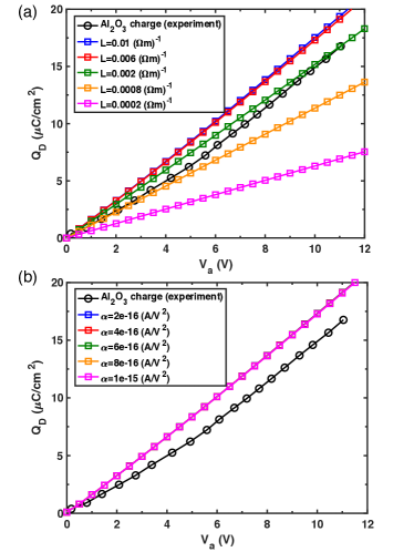
In Fig. 4(a), we show that the experimentally observed charge boost is mainly determined by the kinetic coefficient . The increasing indicates the faster FE charge responses to the applied voltage, leading to larger maximum charges in the same PW. Hence, the release charge can be enhanced with less FE domain viscosity. To further confirm this finding, we also explore the effect of DE leakage and find that the DE leakage is not a dominant factor in the observed charge boost effect, as shown in Fig. 4(b). Note that for simplicity, in Eq. (5) is kept fixed at for all the simulations in this work due to the much less dominant effect in the systems.
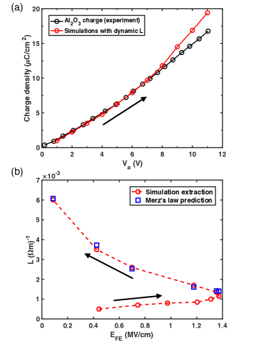
Based on the experimentally measured free charge response from Ref. Hoffmann et al. (2018), the kinetic coefficient can be numerically extracted at a given pulse amplitude. With extracted , Fig. 5(a) demonstrates that the charge boost is enhanced when the applied pulse is large enough to induce the FE response, whereas a small applied pulse only results in the DE response in the FE layer and thus no charge boost is observed. As a reciprocal of the domain viscosity, is assumed to be proportional to the domain wall mobility corresponding to the domain nucleation; that is, . Based on Merz’s law Merz (1956), the relationship between and nonzero can be derived:
| (9) |
where is the domain wall velocity inversely proportional to the switching characteristic time , and is the activation field for domain switching Merz (1956). Fig. 5(b) shows that when the FE is driven into the NC region, can be described by Merz’s law, which suggests the domains are likely to be in the creep region as the electric field across the FE becomes smaller Jo et al. (2009). From Eq. (9), as approaches , is asymptotic to zero because of zero driving force for domain switching. Before FE domain switching, only the DE response is induced, and is found to be linearly dependent on .
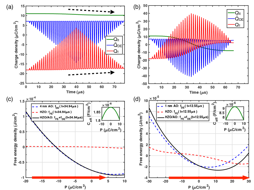
In contrast to the TiN/ HZO/ AO/TiN capacitor, the charge hysteresis was observed in a TiN/ HZO/ AO/TiN capacitor Hoffmann et al. (2018). It was suggested that the appearance of such hysteresis was attributed to the capacitance mismatch between the FE and the DE layer as the DE thickness decreases based on the theory of NC stabilization. However, here we demonstrate that such hysteresis is caused by the DE leakage and the associated interfacial trapped charge dynamics instead of NC stabilization. At the pulse trains with ascending and descending amplitudes, Fig. 6(a) and (b) show the charge responses of the HZO/ AO stack and the HZO/ AO stack, respectively. For the HZO/ AO stack, when a large voltage is across the DE layer, DE leakage is induced and therefore, the trapped charges leak out through the DE, as can be seen from the slightly decreased in Fig. 6(a). As a result, the residual charges of after each pulse gradually increase in Fig. 6(a). For the HZO/ AO stack in Fig. 6(b), the leakage effect becomes more evident compared to the HZO/ AO stack. The simulations indicate that the possible cause of the increasing residual charges after pulse switching experimentally observed in Ref. Hoffmann et al. (2018), especially at a large pulse amplitude, can be explained by the transient responses of trapped charges at the FE-DE interface. Furthermore, from Fig. 6(a) and (b) and Eq. (6), one can infer that the role of the initial DE charge plays in the transient responses is a shift in and dynamics, which means that the choice of the value does not affect the conclusions drawn from the simulations.
The hysteresis behavior can be studied with the curvature of the total free energy profile of the system near polarization reversal. The Landau free energy of the FE in a unit of is given by
| (10) |
The energy stored in a capacitor in terms of can be derived as
| (11) |
where is the DE capacitance per unit area and is the difference between polarization and the DE charges, which is caused by the interfacial trapped charges. Fig. 6(c) and (d) show the free energy profiles of the FE, the DE, and the FE-DE stacks at , where is the time at which is around . Note that in the presence of the trapped charges, the FE and DE energy profiles do not align at because the FE charges are not totally compensated by the DE charges. In the HZO/ AO stack, polarization is switched between one of the energy minimums and the energy maximum, as indicated by the red arrow in Fig. 6(c). In other words, does not go to the other energy minimum state. Note that when is around the energy maximum, the FE is driven into its NC region, where the curvature of the free energy profile (and the FE capacitance) is negative. The effective capacitance of the MFIM system can be obtained by calculating the curvature of the total free energy profile:
| (12) |
From Eq. (12), is positive when the positive DE capacitance is dominant over the negative FE capacitance. With a positive , the NC region gets stabilized and no hysteresis is expected according to the NC theory Salahuddin and Datta (2008); Khan et al. (2016). Note that in Eq. (11) (and thus trapped charges) does not affect the effective capacitance.
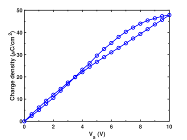
As shown in the inset of Fig. 6(c), the effective capacitance of the AO stack is positive around zero polarization, indicating the FE-DE capacitance match and thus hysteresis-free NC stabilization. For the AO stack, the effective capacitance is also positive around zero polarization, as shown in the inset of Fig. 6(d). Therefore, based on the theory of NC stabilization, such a AO stack is not expected to show hysteresis. However, consistent with the experimental findings in Ref. Hoffmann et al. (2018), the release charge of such a AO stack shows clear hysteresis with the DE leakage parameter in the simulation, as shown in Fig. 7. Note that of the AO stack is larger than that of the AO stack due to the larger leakage current in a thinner DE. In contrast to the AO stack, the FE polarization of the AO stack is driven into the other energy minimum state in the measurement, as indicated by the red arrow in Fig. 6(d). The appearance of hysteresis in the AO stack can be attributed to the increasing FE charge responses due to the larger DE leakage of the thinner DE compared to the AO stack. Therefore, we show that the hysteresis observed in an MFIM stack with a reduced DE thickness is caused not by the FE-DE capacitance mismatch but by the fact that the FE polarization transitions from one state to the other state with the help of DE leakage. This finding is consistent with the previous experimental observation of FE-gated Ge p-channel transistors Zhou et al. (2019). In addition, Fig. 7 shows that, for the MFIM with AO, the maximum release charge difference in the hysteresis at the pulse amplitude of , which is close to the reported value of in Ref. Hoffmann et al. (2018). Note that the hysteresis direction is in a clockwise manner, which is also consistent with the experimental measurements in Ref. Hoffmann et al. (2018).
IV Conclusion
In summary, this paper presents underlying physical mechanisms for the hysteresis-free negative capacitance effect experimentally observed in MFIM capacitors. With the DE leakage and interfacial trapped charges included, we extract the FE parameters by capturing the measured hysteresis loops of MFM capacitors. More importantly, for MFIM stacks, we show (i) the charge boost is mainly determined by the faster FE domain responses near the polarization reversal and (ii) the charge responses would show hysteresis as long as the FE polarization is switched from one state to the other with the aid of DE leakage. The analyses of thermodynamic energy profiles in the presence of interfacial trapped charges indicate that the observed hysteresis in MFIM is caused by the FE polarization switching rather than the FE-DE capacitance mismatch suggested by the theory of NC stabilization. The theoretical demonstrations provide important physical insights into the alleged static NC effect for emerging low-power logic devices.
Acknowledgments
This work was funded by Intel Corporation through Semiconductor Research Corporation MSR-INTEL TASK 2835.001.
References
- Moore (1998) G. Moore, Proceedings of the IEEE 86, 82 (1998), doi: 10.1109/jproc.1998.658762.
- Kim et al. (2003) N. S. Kim, T. Austin, D. Blaauw, T. Mudge, K. Flautner, J. S. Hu, M. Irwin, M. Kandemir, and V. Narayanan, Computer 36, 68 (2003).
- Salahuddin and Datta (2008) S. Salahuddin and S. Datta, Nano Lett. 8, 405 (2008), doi: 10.1021/nl071804g, http://dx.doi.org/10.1021/nl071804g .
- Chang et al. (2017) S.-C. Chang, U. E. Avci, D. E. Nikonov, and I. A. Young, IEEE Journal on Exploratory Solid-State Computational Devices and Circuits 3, 56 (2017), doi: 10.1109/jxcdc.2017.2750108.
- Hsu et al. (2018) C.-S. Hsu, C. Pan, and A. Naeemi, IEEE Electron Device Letters 39, 765 (2018), doi: 10.1109/led.2018.2820118.
- Ni et al. (2018a) K. Ni, P. Sharma, J. Zhang, M. Jerry, J. A. Smith, K. Tapily, R. Clark, S. Mahapatra, and S. Datta, IEEE Transactions on Electron Devices 65, 2461 (2018a).
- Ni et al. (2018b) K. Ni, M. Jerry, J. A. Smith, and S. Datta, in 2018 IEEE Symposium on VLSI Technology (IEEE, 2018) doi: 10.1109/vlsit.2018.8510622.
- Khan et al. (2014) A. I. Khan, K. Chatterjee, B. Wang, S. Drapcho, L. You, C. Serrao, S. R. Bakaul, R. Ramesh, and S. Salahuddin, Nat. Mater. 14, 182 (2014), doi: 10.1038/nmat4148.
- Gao et al. (2014) W. Gao, A. Khan, X. Marti, C. Nelson, C. Serrao, J. Ravichandran, R. Ramesh, and S. Salahuddin, Nano Lett. 14, 5814 (2014), doi: 10.1021/nl502691u.
- Appleby et al. (2014) D. J. R. Appleby, N. K. Ponon, K. S. K. Kwa, B. Zou, P. K. Petrov, T. Wang, N. M. Alford, and A. O’Neill, Nano Lett. 14, 3864 (2014), doi: 10.1021/nl5017255.
- Kim et al. (2016a) Y. J. Kim, H. Yamada, T. Moon, Y. J. Kwon, C. H. An, H. J. Kim, K. D. Kim, Y. H. Lee, S. D. Hyun, M. H. Park, and C. S. Hwang, Nano Letters 16, 4375 (2016a).
- Hoffmann et al. (2016) M. Hoffmann, M. Pešić, K. Chatterjee, A. I. Khan, S. Salahuddin, S. Slesazeck, U. Schroeder, and T. Mikolajick, Adv. Funct. Mater. 26, 8643 (2016), doi: 10.1002/adfm.201602869.
- Chang et al. (2018) S.-C. Chang, U. E. Avci, D. E. Nikonov, S. Manipatruni, and I. A. Young, Phys. Rev. Appl 9 (2018), 10.1103/physrevapplied.9.014010, doi: 10.1103/physrevapplied.9.014010.
- Hoffmann et al. (2018) M. Hoffmann, B. Max, T. Mittmann, U. Schroeder, S. Slesazeck, and T. Mikolajick, in 2018 IEEE International Electron Devices Meeting (IEDM) (IEEE, 2018).
- Hoffmann et al. (2019) M. Hoffmann, F. P. G. Fengler, M. Herzig, T. Mittmann, B. Max, U. Schroeder, R. Negrea, P. Lucian, S. Slesazeck, and T. Mikolajick, Nature 565, 464 (2019).
- Kim et al. (2019) K. D. Kim, Y. J. Kim, M. H. Park, H. W. Park, Y. J. Kwon, Y. B. Lee, H. J. Kim, T. Moon, Y. H. Lee, S. D. Hyun, B. S. Kim, and C. S. Hwang, Advanced Functional Materials 29, 1808228 (2019).
- Hsu et al. (2020) C.-S. Hsu, S.-C. Chang, D. E. Nikonov, I. A. Young, and A. Naeemi, IEEE Transactions on Electron Devices 67, 2952 (2020).
- Böscke et al. (2011) T. S. Böscke, J. Müller, D. Bräuhaus, U. Schröder, and U. Böttger, Appl. Phys. Lett. 99, 102903 (2011), doi: 10.1063/1.3634052.
- Müller et al. (2012) J. Müller, T. S. Böscke, U. Schröder, S. Mueller, D. Bräuhaus, U. Böttger, L. Frey, and T. Mikolajick, Nano Lett. 12, 4318 (2012), doi: 10.1021/nl302049k.
- Sharma et al. (2017) P. Sharma, K. Tapily, A. K. Saha, J. Zhang, A. Shaughnessy, A. Aziz, G. L. Snider, S. Gupta, R. D. Clark, and S. Datta, in 2017 Symposium on VLSI Technology (IEEE, 2017) doi: 10.23919/vlsit.2017.7998160.
- Kobayashi et al. (2016) M. Kobayashi, N. Ueyama, K. Jang, and T. Hiramoto, in 2016 IEEE International Electron Devices Meeting (IEDM) (IEEE, 2016) doi: 10.1109/iedm.2016.7838402.
- Alam et al. (2019) M. A. Alam, M. Si, and P. D. Ye, Appl. Phys. Lett. 114, 090401 (2019), doi: 10.1063/1.5092684.
- Liu et al. (2020) Z. Liu, H. Jiang, B. Ordway, and T. P. Ma, IEEE Electron Device Letters 41, 1492 (2020).
- Merz (1956) W. J. Merz, Journal of Applied Physics 27, 938 (1956).
- Tagantsev (2008) A. K. Tagantsev, Ferroelectrics 375, 19 (2008), doi: 10.1080/00150190802437746.
- Landau (1937) L. D. Landau, Zh. Eksp. Teor. Fiz 7, 19 (1937).
- Ginzburg (1945) V. L. Ginzburg, Zh. Eksp. Teor. Fiz 15, 739 (1945).
- Devonshire (1949) A. Devonshire, The London, Edinburgh, and Dublin Philosophical Magazine and Journal of Science 40, 1040 (1949), doi: 10.1080/14786444908561372.
- Si et al. (2019) M. Si, X. Lyu, and P. D. Ye, ACS Applied Electronic Materials 1, 745 (2019).
- Lin et al. (2005) H. C. Lin, P. D. Ye, and G. D. Wilk, Applied Physics Letters 87, 182904 (2005).
- Pešić et al. (2016) M. Pešić, F. P. G. Fengler, L. Larcher, A. Padovani, T. Schenk, E. D. Grimley, X. Sang, J. M. LeBeau, S. Slesazeck, U. Schroeder, and T. Mikolajick, Advanced Functional Materials 26, 4601 (2016).
- Kim et al. (2016b) H. J. Kim, M. H. Park, Y. J. Kim, Y. H. Lee, T. Moon, K. D. Kim, S. D. Hyun, and C. S. Hwang, Nanoscale 8, 1383 (2016b).
- Chouprik et al. (2019) A. Chouprik, M. Spiridonov, S. Zarubin, R. Kirtaev, V. Mikheev, Y. Lebedinskii, S. Zakharchenko, and D. Negrov, ACS Applied Electronic Materials 1, 275 (2019).
- Goh et al. (2020) Y. Goh, S. H. Cho, S.-H. K. Park, and S. Jeon, Nanoscale 12, 9024 (2020).
- Lomenzo et al. (2020) P. D. Lomenzo, C. Richter, T. Mikolajick, and U. Schroeder, ACS Applied Electronic Materials 2, 1583 (2020).
- Jo et al. (2009) J. Y. Jo, S. M. Yang, T. H. Kim, H. N. Lee, J.-G. Yoon, S. Park, Y. Jo, M. H. Jung, and T. W. Noh, Physical Review Letters 102 (2009), 10.1103/physrevlett.102.045701.
- Khan et al. (2016) A. I. Khan, U. Radhakrishna, K. Chatterjee, S. Salahuddin, and D. A. Antoniadis, IEEE Transactions on Electron Devices 63, 4416 (2016).
- Zhou et al. (2019) J. Zhou, G. Han, N. Xu, J. Li, Y. Peng, Y. Liu, J. Zhang, Q.-Q. Sun, D. W. Zhang, and Y. Hao, IEEE Electron Device Letters 40, 329 (2019).