Scalable first-principles-informed quantum transport theory in two-dimensional materials
Abstract
Accurate determination of carrier transport properties in two-dimensional (2D) materials is critical for designing high-performance nano-electronic devices and quantum information platforms. While first-principles calculations effectively determine the atomistic potentials associated with defects and impurities, they are ineffective for direct modeling of carrier transport properties at length scales relevant for device applications. Here, we develop a scalable first-principles-informed quantum transport theory to investigate the carrier transport properties of 2D materials. We derive a non-asymptotic quantum scattering framework to obtain transport properties in proximity to scattering centers. We then bridge our scattering framework with perturbation theory, with inputs from first-principles electronic structure calculations, to construct a versatile multiscale formalism that enables modeling of realistic devices at the mesoscale. Our formalism also accounts for the crucial contributions of decaying evanescent modes across heterointerfaces. We apply this formalism to study electron transport in lateral transition-metal dichalcogenide (TMDC) heterostructures and show that material inclusions can lead to an enhancement in electron mobility by an order of magnitude larger than pristine TMDCs.
I Introduction
Nanoelectronic devices, based on low-dimensional materials offers avenues to construct integrated circuits beyond the limits of Moore’s law Li ; Shalf ; ashwin . Atomically thin monolayers such as graphene Schwierz , silicene Akinwande , phospherene zhang_phospherene , and transition metal dichalcogenides (TMDC) Salahuddin ; Cui ; Bartolomeo have all been explored to construct high-performance field effect transistors, and these two-dimensional (2D) materials have shown great potential to succeed silicon in the next-generation computers. However, accurate prediction of transport properties in these materials is a crucial challenge that must be overcome before they can be used in practical devices Li .
Electron scattering due to imperfections, dopants/impurities, and phonons determine the carrier dynamics in 2D materials. Carrier transport properties can also be engineered by creating potential patterns and quantum confinements, such as through the application of local potentials via STM/AFM tips Levitov ; Pasupathy , surface functionalization by organic molecules ashwinNaveh ; Margapoti ; ulloa1 , or through spatial confinement in lateral heterostructures shenoy . Density-functional theory (DFT) kohnsham provides a parameter-free method for electronic structure calculations and the accurate determination of atomistic potentials associated with heterointerfaces, defects, and impurities. However, DFT is ineffective for direct modeling of carrier transport properties at length scales relevant to device applications. There have been efforts to provide an atomistic quantum transport framework based on tight-binding methods kwant , plane-wave representation of empirical pseudopotentials Vandenberghe , and DFT-based non-equilibrium Green’s function techniques Taylor ; Brandbyge . However, such simulations can become computationally expensive with increasing number of atoms. Moreover, scattering across the material interfaces have significant contributions from the decaying evanescent modes, which traditional scattering calculations do not account, since the probabilities of evanescent modes vanish in the asymptotic limit where the boundary conditions (BCs) are applied to determine the scattering amplitudes. Hence, we require a more detailed scattering framework where the scattering properties are evaluated in proximity to scattering centers.
In this article, we present a framework for first-principles-informed continuum quantum transport theory. We develop a non-asymptotic quantum scattering theory, and show that bridging our scattering theory framework and the perturbation theory, using inputs from ab-initio electronic structure calculations provides a versatile multiscale formalism. In particular, we envision immediate applications of our theory in simulations and design of electron optics, and in nanoscale optoelectronic platforms.
This article is organized as follows. In Sec. II, we develop a non-asymptotic quantum scattering theory based on sources and absorbers. With this setup, we obtain the total wavefunction that includes both propagating and evanescent band contributions. This formalism is then extended to a multiband framework, by integrating with it the perturbation theory using inputs from DFT calculations, as explained further in Sec. III. In that section we also explain the method to include thermal properties in our formalism through deformation potentials obtained via DFT calculations. In Sec. IV, we apply our formalism to study transport properties in lateral TMDC heterostructures. We observe the emergence of Fano resonances in 2D materials with material inclusions. We also show the enhancement of electron mobility in lateral heterostructures comprised of combinations of TMDC monolayers. Concluding remarks are presented in Sec. V.
II Construction of Sources and Absorbers
The traditional treatment of scattering employs an ad-hoc condition that the distance between scattering centers and the observer is asymptotically large. At large distances, the solution wavefunction is expressed as a linear combination of the incoming and outgoing basis functions with undetermined amplitudes. A partial wave analysis is then performed in the asymptotic limit to obtain these amplitudes in terms of the phase-shift parameters. For example, in the 3D open domain, the wavefunction is expressed in terms of the spherical Hankel functions of the first kind Adhikari1 . We can then easily deduce the scattering amplitudes since all Hankel functions have the same asymptotic form given by , which represents the outgoing spherical wave sommerfeld . Lord Rayleigh rayleigh developed this method for the first time in the context of acoustic scattering, and later it was extended to quantum mechanics by Faxen and Holtsmark faxen .
In the asymptotic limit, only the radial component of the scattered current contributes to the cross-section. As a result, information about the angular current contributions cohenTannoudji , and the distance between target and observer is lost in this analysis. In reports by Dai et al.,dai1 ; dai2 it has been shown that a rigorous scattering treatment without the asymptotic approximations introduces a modification factor to the scattering amplitude, and an additional phase factor to the scattered wavefunction. Hence, our first aim is to formulate a framework to obtain the scattering properties without applying asymptotic BCs. In the conventional variational formulation of the scattering theory, asymptotic BCs are applied either by mapping the far-field partial wave expansion into the near-field region porod or by approximating the Sommerfeld radiation conditions sommerfeld ; ludwig . However, both of these approaches fail to account for the decaying evanescent solutions, since they inherit the asymptotic BCs.
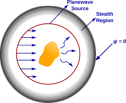
Previously, for electron scattering in waveguides, we proposed a method to reduce the scattering BCs to Dirichlet BCs by creating absorbers (stealth regions) on either end of the waveguide sathwik1 . An extension of this technique to 2D open domain is achieved here by creating circular absorbers around the scattering center, as shown in Fig. 1. Within the absorber, we perform a coordinate transformation , and an energy transformation . Here, is the cubic Hermite interpolation polynomial varying smoothly from to . Through such transformation, it has been shown that the no-reflection condition is satisfied sathwik1 and the absorber will not reflect any wave back into the active region confined within the absorber. Therefore, scattering properties in the active region remain unaffected by the presence of the absorber. As a result of such a transformation, the wavefunction decays rapidly within the absorber, and we can apply Dirichlet BCs at the boundary of the absorber. Through this technique, we can confine the computational domain, while preserving the near-field nature of the wavefunction in the region confined by the absorber (scattering region), that is otherwise lost due to the application of asymptotic BCs.
Once we enclose the active scattering region with the absorber, we require a source (an electron antenna) in the active region to initiate the incoming plane waves (see Fig. 1). This is achieved by introducing a source term in the Schrödinger equation. In order to derive this source term, we start with the Green’s function equation for the Schrödinger operator in the 2D circular coordinate system given by
| (1) |
where is the source term whose form is yet to be determined, the wavevector , is the incoming energy, and is the effective mass. We expand the Green’s function in the Fourier representations as
| (2) |
Inserting this Fourier expansion into Eq. (II) we obtain
| (3) | ||||
Multiplying Eq. (3) by and integrating over , from to , we obtain
| (4) |
The radial part is the Green’s function for the one-dimensional Sturm Liouville operator MorseFeshbach and will be of the form
| (5) |
where, and are the Bessel and Hankel function of first kind, respectively. We determine the coefficient by applying the jump condition at given by
| (6) |
where, the Wronskian . Thus,
| (7) |
Substituting Eqs. (5) and (7) into Eq. (2), we obtain the total Green’s function of the form
By using the addition theorem for Bessel functions MorseFeshbach we have
| (8) |
We note that represents the wave originating from the point source at . As shown in Fig. 1, to obtain a circular source we integrate over the angular coordinate from to . Hence the wavefunction emerging from the circular source is given by
| (9) |
Our aim is to generate plane waves propagating in the forward direction from the circular source within the region . Hence, we choose the source term to be
| (10) |
Now, substituting Eq. (10) into Eq. (9) we obtain
| (11) |
where we have utilized the orthogonal properties of the function . We know the expansion of plane wave . Hence,
| (12) |
and we obtain plane waves impinging on the scattering center from a circular source at , as shown in Fig. 1. The wavefunction in the region will simply be absorbed by the stealth region.
Once we formulate the quantum scattering theory with the source and absorber, we can employ numerical methods to solve Eq. (II) and obtain the total wavefunction . In the presence of a scattering potential, we obtain the total wavefunction . Here, includes both the radial and angular current contributions. In particular, also includes the evanescent solutions in case of an absorbing scattering potential or in case of multiband scattering processes, as discussed in the next section.
Throughout this article, we have solved the Hamiltonian equation by casting it into an action integral. This action integral is solved using finite element analysis (FEA) ram_book ; Zienkiewicz ; jin ; ramfem . In FEA, we discretize the physical domain of interest into small elements. Within each element, we express the wavefunction as a linear combination of interpolation polynomials multiplied by undetermined coefficients. These coefficients correspond to the value of the wavefunction and their derivatives at the vertices (nodes) of the element. With this approach, one can systematically increase the accuracy through mesh size refinement (-refinement) or by employing higher order interpolation polynomials (-refinement).
To validate our scattering formalism, we consider the case of 2D scattering from a hard circle. The hard circle potential is given by
| (13) |
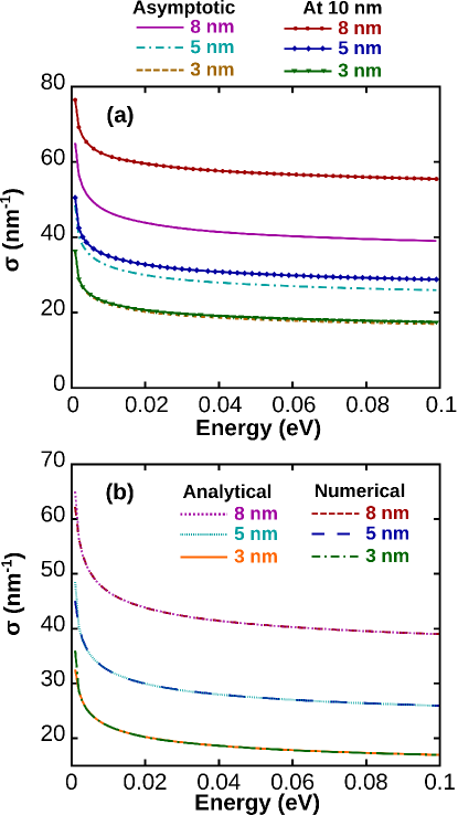
where, is the radius of the circle. Through partial-wave analysis, we can obtain a closed-form result for the scattering cross-section length, , measured at the asymptotic distance (see Appendix B). In Fig. 2(b), we compare the analytical result (see Eq. (56)), and the result obtained through our formalism. The behavior of at low- and high-energy limits, observed in Fig. 2(b), is discussed in Appendix B.
In Appendix A, we outline the scattering theory without applying asymptotic boundary conditions dai1 ; dai2 . In Fig. 2(a), we compare the cross-section length obtained by an observer at a very large distance (asymptotic limit) and by an observer at a finite distance of nm, and find a significant quantitative difference. In case of the hard circle potential, difference between the asymptotic and non-asymptotic predictions increases with decreasing distance between the observer and the hard circle. In Fig. 2(a), we see that the deviation between the prediction at the asymptotic limit, and for the observer at nm is maximum for the hard circle radius of nm. This is because the effective distance from the hard circle and the observer is least for the nm potential, amongst the considered hard-circle radii. Thus confirming that in nanoscale systems, it is especially important to employ the non-asymptotic scattering theory developed here to obtain accurate transport properties. In Appendix C, we derive the source term for the non-asymptotic scattering theory in three-dimensions (3D). Such analysis in 3D can be employed to obtain transport properties in bulk materials.
III Envelope function scattering theory with sources and absorbers
In multiband scattering processes, the wavefunction will have contributions from not only the propagating waves, but also from the exponentially decaying evanescent waves sathwik1 . This is particularly prevalent in transport across heterointerfaces.
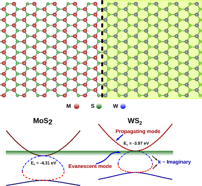
For example, in Fig. 3, we consider a heterointerface formed between MoS2 and WS2 monolayers. From first-principles electronic structure calculations, we know that MoS2 (eV) has a lower conduction band minimum than WS2 (eV) monolayer. Hence, when an electron with energy eVeV is injected from the MoS2 to the WS2 monolayer, transport can occur only through the evanescent modes. These evanescent modes are placed within the bandgap and will have purely imaginary wavevectors, which in turn results in exponentially decaying contributions to the scattered wavefunction. Traditional scattering calculations cannot account for these crucial contributions, since the probabilities of evanescent modes vanish at the asymptotic limit where the boundary conditions are applied to determine the scattering amplitudes. We therefore require a new quantum scattering framework as discussed in Sec. II, that can accurately compute both the evanescent modes and angular current contributions in the near-field of the scattering center.
The low-energy dynamics of charge carriers in semiconductors can be effectively described by the Hamiltonian luttingerkohn ; luttinger ; bir_pikus ; Dresselhaus . This Hamiltonian provides an accurate characterization of the energy dispersion around the high-symmetry points of the Brillouin Zone, in terms of a small number of input band parameters. These band parameters, in turn, can be obtained from accurate first-principles calculations, for example, DFT or many-body perturbation theory C2DB . In this section, we describe the multiband scattering theory using the envelope functions solutions of the Hamiltonian.
The Hamiltonian effectively captures the coupled dynamics of the conduction and valence bands around the high-symmetry points of the Brillouin zone. This is also the region in which we are most interested in determining the transport properties. Effects of remote bands can be easily included by using Löwdin perturbation theory lowdin . Effects due to strain, magnetic field, and spin-orbit coupling can also be included as additional input parameters. Being a long-wavelength theory, perturbation theory is well suited to simulate transport properties at device-relevant scales.
Let us consider the Hamiltonian equation of the form
| (14) |
where is the source term defined in Eq. (10), is the incoming amplitude, is the band-index, is the wavevector, and is a scale factor (derived in Appendix E). Here, is the cell periodic potential, and is the defect/impurity potential obtained from DFT calculations. In the envelope-function approximation (EFA), the general form of the wavefunction and the incoming amplitude are considered as a linear combination of a finite number of bands luttingerkohn ; kane1 ; kane2 , given by
| (15) |
where is the slowly-varying envelope function, is the cell-periodic Bloch function, is the incoming amplitude, and is the number of bands considered. Here, the expansion is at a fixed value, and we will assume from now on that the expansion is around . Within the framework of EFA, we perform ‘cell-averaging’ by integrating over each unit cell of the crystal. Bloch functions satisfy Schrödinger’s equation with band-edge energies, and results in:
| (16) |
where is the momentum matrix element. This averaging procedure results in equation of the form
| (17) |
where is the Hamiltonian, and is the identity matrix. From now on we denote simply as . The envelope function is , and the incoming amplitude is . In the absence of the defect potential , the incoming amplitudes satisfy an equation of the form
| (18) |
Hence, for a given energy, we can obtain by solving the above eigenvalue equation. Note that Eq. (18) represents the standard Hamiltonian equation for the pristine material.
We cast Eq. (17) into an action integral, as this allows us to solve the equation in the variational approach. The advantages of the action integral formulation are that there is no ambiguity about reordering of operators for symmetrization lrr_wavefunction and, moreover we can easily evaluate the conserved current using the gauge-variational approach introduced by Gell-Mann and Levy gellmanlevy and used extensively by us lrr_wavefunction (see Appendix (D)). This action integral is solved using finite element analysis. A detailed discussion of this variational numerical procedure is described in our earlier work sathwik1 .
Within the Boltzmann transport formalism, important transport properties such as the mobility, conductance and Seebeck coefficients are expressed in terms of the total relaxation time . To determine , we need to consider both the intrinsic and extrinsic scattering rates. The extrinsic scattering rate arises from the potential scattering. According to Matthiessen’s law
| (19) |
where, is the extrinsic carrier scattering time and is the total intrinsic scattering time arising from the acoustic and optical phonon mode contributions.
III.1 Carrier scattering time
Through kinectic theory liboff , for elastic scattering processes in 2D, is given by
| (20) |
where is the disorder density, is the average velocity, and is the momentum scattering cross-section defined as
| (21) |
where, is the differential cross-section length. The average incident velocity is
| (22) |
where is the carrier velocity, and is the angle between the velocity vector and the longitudinal axis. For example, for a uniform velocity distribution, .
III.2 Phonon scattering time
First-principles calculations provide a convenient way of determining the phonon scattering times by computing the deformation potentials of the crystal lattice Bardeen . In 2D materials, the phonon scattering rate from the longitudinal and transverse acoustic phonons is given by Kaasbjerg ; kim_eph ; kim_eph_mos2
| (23) |
where is the effective mass, is the first-order deformation potential, is the absolute temperature, is the 2D ion mass density, and is the sound velocity of the acoustic phonons. The intervalley acoustic phonon and optical phonon rates are expressed in terms of the zero-order deformation potential , and is given by
| (24) |
where is the Heaviside step function, is the phonon frequency, and is the Bose-Einstein distribution function for the phonon mode . Effect of the Fröhlich interaction can be implicitly added to the deformation potential kim_eph . We neglect the first-order optical deformation potential contributions, that are typically small compared to the values from Eqs. (23) and (24). Hence the total intrinsic phonon scattering rate is computed by summing over the all phonon modes, .
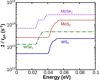
In Fig. 4, we have plotted the total intrinsic phonon scattering rate at room temperature for various TMDC monolayers. We have included deformation potentials for the acoustic and optical phonon modes corresponding to the transition, . Emergence of contributions from optical phonon modes are observed as steps in the scattering rate. We observe that MoSe2 (WS2) has the strongest (weakest) interaction with phonons for the considered TMDC monolayers. WX2 has a greater electrical conductivity than MoX2. These observations and scattering rate values are consistent with previous first-principles study in the literature Kaasbjerg ; kim_eph .
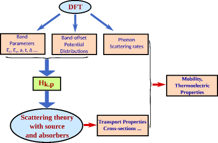
The flowchart displayed in Fig. 5 summarize the quantum transport framework discussed in this article. The band parameters, potential distributions, and phonon scattering rates are obtained through DFT calculations. These quantities will be an input to the Hamiltonian which is then solved using the non-asymptotic quantum scattering theory. By combining the carrier scattering rate obtained through our calculations with the phonon scattering rate obtained though first-principles calculations, we can accurately obtain the carrier mobility and thermoelectric performance of the devices. In our theory, the scattering properties are calculated at a finite distance from the scattering center. Hence, it will accurately account for the evanescent mode contributions that are significant in scattering across heterointerfaces. This is evident from the enhancement of the electron mobility observed here, for TMDC monolayers with material inclusions.
IV Transport properties in TMDC heterostructures
Transition-metal dichalcogenides have attracted tremendous recent interest in fabricating 2D semiconductor nanoelectric circuits kis1 ; kis2 ; kis3 . In contrast to graphene, TMDCs host massive Dirac fermions due to their direct bandgap, which negates the probability of Klein tunneling ulloa_hardcirlceTMD . Strong coupling between spin and valley degrees of freedom are observed in TMDC monolayers due to their lack of inversion symmetry cui1 . This makes them interesting candidates to realize valleytronic devices as well ye .
Similar crystal structures and comparable lattice constants observed in MX2 (M = Mo, W; X = S, Se) monolayers have motivated the study of TMDC-based quantum confinement in heterostructures shenoy ; Kormanyos ; Liu_pang ; Wu_tong ; Pawlowski ; Pisoni ; ulloa_ovando . Experimentally, such lateral heterostructures can be realized through multistep chemical vapor deposition techniques, bottom up synthesis, and micromechanical techniques growth1 ; growth2 ; growth3 ; growth4 ; growth5 ; growth6 ; growth7 ; growth8 ; growth9 ; growth10 . The ability to pattern material inclusions in these systems provides an enhanced level of control over their electrical properties. Hence, they have great potential to realize in-plane transistors, photodiodes, cascade lasers, and CMOS circuits.
As shown in Fig. 3, the mismatch between band-offsets breaks the translational symmetry within planar TMDC heterostructures. Hence the evanescent modes (with purely imaginary wavevector) contribute heavily to their transport properties. Therefore, in 2D lateral heterostructures, the carrier scattering calculations have to carried out using the method described in Sec. III. In TMDCs, a seven-band model can accurately capture the most important dispersion features of the conduction (CB) and valence (VB) bands kormanyos1 . We can apply Löwdin perturbation theory lowdin to reduce the seven band model into a two-band model corresponding to the lowest CB and highest VB. Here, we keep the terms up to second-order in the diagonal element in the Hamiltonian corresponding to the basis set . Here, is the spin index, and denotes the valley . symmetry dictates that the Hamiltonian should have the form
| (25) |
where denotes the Pauli matrices, is the lattice constant, is the effective hopping integral, is the spin-orbit (SO) parameter, and is given by
| (26) |
Here, are the material parameters, and and are the CB minimum and the VB maximum, respectively. As the theory is corrupted with the occurrence of spurious solutions, we have utilized the Foreman transformations foreman to eliminate the spurious solutions, and hence, we set . In Table 1 we have listed all the parameters used in our calculations for MoS2, WS2, MoSe2, WSe2 monolayers. For now we have neglected strain matrix elements since MoS2 (MoSe2) and WS2 (WSe2) have commensurate lattice constants. Material parameters between the two layers are smoothly interpolated through the self-consistent potential distribution obtained from DFT calculations.
| (eV) | (eV) | (Å) | (eV) | (eV) | (eVÅ2) | |
|---|---|---|---|---|---|---|
| MoS2 | -4.31 | -5.89 | 3.184 | 1.059 | 0.073 | -5.97(-6.43) |
| WS2 | -5.97 | -5.50 | 3.186 | 1.075 | 0.211 | -6.14(-7.95) |
| MoSe2 | -3.91 | -5.23 | 3.283 | 0.940 | 0.090 | -5.34(-5.71) |
| WSe2 | -3.61 | -4.85 | 3.297 | 1.190 | 0.230 | -5.25(-6.93) |
IV.1 Fano Resonance
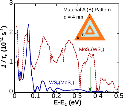
In Fig. 6, we have plotted the electron scattering rate for a 2D triangular superlattice between MoS2 and WS2 monolayers. There have been experimental efforts to realize such structures through lateral epitaxy growth9 . MoS2 has a lower CB minimum as compared to WS2. Hence, below eV (marked by a green arrow in Fig. 6) transport in WS2 layers can occur only through the evanescent modes. Evanescent wavevectors are the purely imaginary roots of the Hamiltonian defined in Eq. (25). Firstly, we observe that the WS2 (MoS2) structure has a lower scattering rate (higher lifetime) as compared to the MoS2 (WS2) structure. This is because an electron injected from the WS2 layer can scatter through the additional propagating conduction channel available from MoS2 inclusions. For transport in the MoS2 (WS2) structure, we observe that at the incoming energies eV (eV, marked by an arrow in Fig. 6), corresponding to the CB minimum of WS2, the electron scattering rate decreases significantly, since the evanescent modes disappear above this energy. The resonances observed in the MoS2 (WS2) structure, below the energy eV are due to the interaction with the trapped electron states within the WS2 barrier.
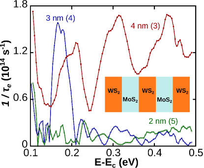
For transport in the WS2 (MoS2) structure, we observe both a maximum and minimum in the electron scattering rate around eV (see Fig. 6). This marks the occurrence of a Fano resonance in the transmission profile, an effect analogous to that of atomic autoionization Fano , first observed in the context of inelastic electron scattering by a helium atom. Analogous Fano profiles are observed around the subband minima of a quantum waveguide with attractive potentials sathwik2 . Here, the MoS2 inclusion acts as a quantum well and leads to the formation of quasi-bound metastable states. Interaction between the propagating modes and the quasi-bound states leads to the Fano resonance. Multiple Fano resonances are observed when we have a superlattice of WS2 and MoS2 layers as shown in Fig. 7. Formation of Fano resonances leads to an enhancement in the thermoelectric figure-of-merit far beyond the pure 2D monolayers. This phenomenon will be discussed in detail elsewhere sathwik_thermoelectric .
IV.2 Enhancement of Electron Mobility
In this section, we study the electron mobility in TMDC heterostructures. Around the -valley, the CB is isotropic and parabolic in nature. Hence, the mobility can be defined as
| (27) |
where, the 2D carrier density , is the density of states, and the Fermi-Dirac distribution is . Due to the parabolic nature of CB, we consider constant , where and ( for VB, CB) are the spin and valley degeneracies, respectively.
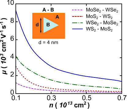
In Fig. 8, we plot the total electron mobility (including both phonon and electron contributions) at room temperature for the -type TMDC monolayers with triangular inclusions. The density of triangular inclusions is considered to be cm-2. We observe an enhancement in the mobility at low carrier density. The WS2 monolayer with MoS2 inclusion has the highest mobility amongst the considered combinations. This can be attributed to two main factors: 1) additional CB channels available from MoS2 inclusions enhance the electron scattering lifetime, 2) WS2 monolayer has the highest phonon scattering lifetime amongst the family of TMDC monolayers (see Fig. 4). The MoS2 monolayer with WS2 inclusion, on the other hand has lower mobility. This is because the evanescent modes, being real functions, will not contribute to the probability current, thereby suppressing the overall mobility. We also note that the mobility observed here in WX2 monolayers with triangular inclusions is an order of magnitude larger than the phonon-limited mobility and the mobility calculated in layers with charged vacancies. In charged vacancies, Coulomb contributions suppress the mobility tonylow . Hence, short-range potentials such as the inclusions considered here are very promising candidates to realize high-mobility devices.
V Conclusions
In this article, we have developed a non-asymptotic quantum scattering theory using a novel method of sources and absorbers. The Cauchy boundary conditions that are necessary in the variational formulation of scattering are reduced to simpler Dirichlet boundary conditions by constructing a perfect absorber (stealth region) around the scattering centers. This allows us to define a finite computational domain. In the conventional scattering theory, scattering properties are determined at the asymptotic distance, resulting in the loss of evanescent mode contributions in multiband scattering processes and in the presence of absorbing scattering potentials. Introducing an absorber facilitates the evaluation of the scattering properties at a finite distance, and preserves the distance information between the observer and the scattering center. Once we enclose the active scattering region with the absorber, we require a carrier source to generate plane-waves and initiate the scattering event. We have derived the expression for the circular source term in Eq. (10) introduced in the right-hand side of the Hamiltonian equation.
We have shown that even for the simplest case of scattering from a hard circle potential, the cross-section length measured at a finite distance using our formalism, and at the asymptotic distance obtained through the analytical formulation show significant quantitative differences. As the carrier scattering time is inversely proportional to the cross-section length, our formalism is of immediate relevance in nanoscale systems, where transport measurements are made in proximity to the scattering centers.
We have shown that bridging our scattering theory framework with the perturbation theory, with inputs from ab-initio electronic structure calculations, provides a versatile multiscale formalism. The continuum nature of our formalism enables the modeling of realistic devices, scaling from hundreds to thousands of atoms. Carrier scattering rates obtained through our formalism combined with the phonon scattering rates obtained through DFT calculations can accurately calculate the thermoelectric properties of the nano-devices.
We obtained the phonon scattering rates for MX2 (M = Mo, W; X = S, Se) monolayers through deformation potential calculations. We observed that the WS2 (MoSe2) has the highest (lowest) phonon scattering time in the family of MX2 monolayers. This observation is consistent with other first-principles study in the literature. As an application of our formalism, we studied the transport properties in lateral TMDC heterostructures. Material inclusions in TMDCs acts as a short-range scattering centers. We observed the emergence of novel Fano resonances for the first time in 2D materials, when MoS2 is encapsulated within WS2 monolayer. The MoS2 inclusion here acts as a quantum well, and forms the quasi-bound states that interact with the propagating modes leading to these resonances.
Lastly, we studied mobility of electrons as a function of carrier density in a family of TMDC layers with triangular inclusions. Here, WS2 monolayer with MoS2 inclusions is observed to have the highest electron-mobility, which is by an order of magnitude larger than the phonon-limited mobility. Hence, such lateral TMDC heterostructures should be explored as candidates to realize high-mobility devices.
Acknowledgements.
Calculations presented here were performed using computational resources supported by the Academic and Research Computing Group at WPI.Appendix A Scattering cross-section length at a finite distance
The differential cross-section is determined by dividing the scattered flux by the incoming flux, given by
| (28) |
where is the scattered current, and is the magnitude of the current from the incoming plane wave. In the traditional scattering theory, the detector is at infinity, and the outgoing wave in 2D is a circular wave of the form . When the observer is at a finite distance, , the outgoing wave-front incident on the observer will have both radial and angular components. The surface element is considered to be orthogonal to the outgoing current dai1 ; dai2 . In a 2D scattering,
| (29) |
where is the determinant of the metric . In 2D circular coordinate system
| (30) |
Hence,
| (31) |
where
In order to compare with the expression given in the standard scattering theory, we would like to express the scattered flux in Eq. (31) only in terms of the scattering current components. We know that
| (32) |
Hence we can express the scattered current as
| (39) |
Now let us take a surface of revolution for the scattered current, expressed in a parametric form . The tangential vector at a point on this surface is
| (40) |
and the normal vector is
| (43) |
Hence, the scattered current is given by
| (44) | ||||
| (47) |
Equating Eq. (39) and (44), we obtain the angular components of the scattered as
| (48) |
Hence we find that
| (49) |
By substituting this relation in Eq. (31), we obtain
| (50) |
We know that . Substituting this relation to Eq. (31) we obtain
and the differential cross-section length is given by
| (51) |
Note that as the source and observer are pushed to infinity ,
| (52) | ||||
where is scattering amplitude. Hence, we obtain the standard definition of the differential cross-section length Adhikari1 in the limit .
Appendix B Scattering from a Hard circle potential
In this appendix, we discuss the analytical results for the scattering from a hard circle potential in 2D. Even though, this problem has been addressed before in the literature Lapidus ; Shertzer , the limiting behavior has not been discussed.
The hard circle potential of radius in a 2D space is given by
| (53) |
The solution wavefunction for the above potential is of the form
| (54) |
To determine the coefficients , we utilize the boundary condition . Hence,
| (55) |
where we have used the expansion of the planewave . Through partial-wave analysis, we obtain the total cross-section length given by
| (56) |
To compare the quantum mechanical calculations with classical mechanics predictions, we consider the cross-section length in the high energy limit . We know that,
| (57) |
Therefore,
| (58) |
Classically, the particle will not be deflected by the potential if the impact parameter . The angular momentum will follow the limit . Hence, we can restrict the sum in Eq. (58) between the limits . With this simplification, we obtain the cross-section length
| (59) |
which is twice the classical mechanics prediction Lapidus .
To obtain the low energy limit () of the cross-section length, we retain only the first term () in the series given in Eq. (56). In this limit,
| (60) |
Hence,
| (61) |
This is not an analytic function. Therefore, as , cross-section length will diverge even though the scattering current vanishes.
Appendix C Scattering theory in three-dimensions using sources and absorbers
In this appendix, we set up the framework for the quantum scattering theory in 3D, using our source and absorber scheme. In 3D, we consider a spherical source, and the absorber will be a spherical shell. An incoming plane wave will be of the form
| (62) |
where, are the Laplace spherical harmonics, are the spherical Bessel function, and define the direction of the wavevector . Following a similar scheme as in Sec. II, we can derive the corresponding source term
| (63) |
where, is the spherical Hankel function. With this set up the incoming wavefunction in the absence of external potential is given by
Hence, we obtain plane waves incident on the scattering center from a spherical source at .
Appendix D Action integral formation
In this appendix, we explain the action integral formulation employed to solve Eq. (17). Let us consider a general form of the Hamiltonian in a 2D material given by
| (64) |
where are the coefficient matrices, , and . For simplicity, we have considered only the terms up to the second order derivatives. With this Hamiltonian, the action integral corresponding to Eq. (17) is given by
| (65) |
where is the Lagrangian operator given by
where and represent the derivative operator acting on the functions appearing to the left and right side, respectively. This will ensure the correct operator ordering at the material interface lrr_wavefunction .
Across a material interface, the envelope wavefunction, and the probability current has to be continuous. The continuity of the envelop function is ensured by using Hermite interpolation polynomials in our calculations, which will have both first and second derivative continuity KBR . The probability current is evaluated using a gauge-variational approach that is commonly used in high energy/particle physics. Following Gell-Mann and Levy gellmanlevy , we perform a transformation of the envelop function with respect to an arbitrary gauge function of the form, . With this transformation, we obtain the conserved current
| (66) |
The interfacial potential is obtained from the DFT calculations, and will be continuous across the interface. Hence, this conserved current will also be continuous.
Appendix E Scale factor
In this appendix, we obtain the expression for the scale factor employed in Eq. (17). For simplicity, let us consider the Hamiltonian in one-dimension (1D). The expression we obtain here for 1D translates into higher dimensions as well. Let us consider the equation
| (67) |
where the source term in 1D is given by sathwik1 ; ram_book , with being the incoming wavevector. The solution to the above equation in terms of the Fourier components is given by
| (68) |
Let us constrain to be a matrix, with eigenenergies given by and . Then
| (69) |
where are the solution wavevector for the determinantal equation . The Hamiltonian can include terms in higher order (such as ) and hence, the determinant equation will have roots. Therefore, we choose
| (70) |
so that the the incoming wavefunction will have the form
| (71) |
The expression derived in Eq. (70) follows for 2D and higher dimensions as well.
References
- (1) M-Y. Li, S-K. Su, H.-S. P. Wong and L.-J. Li, Nature 567, 169–170 (2019)
- (2) J. M. Shalf and R. Leland, Computer 48, 14–23 (2015)
- (3) F. Xia, H. Wang, D. Xiao, M. Dubey, A. Ramasubramaniam, Nat. Photon. 8, 899–907 (2014).
- (4) F. Schwierz, Nat. Nanotechnol. 5, 487–496 (2010).
- (5) L. Tao, E. Cinquanta, D. Chiappe, C. Grazianetti, M. Fanciulli, M. Dubey, A. Molle and D. Akinwande, Nat. Nanotechnol. 10, 227–231 (2015).
- (6) L. Li, Y. Yu, G. Jun Ye, Q. Ge, X. Ou, H. Wu, D. Feng, X. H. Chen and Y. Zhang, Nat. Nanotechnol. 9, 372–377 (2014).
- (7) Y. Yoon, K. Ganapathi, S. Salahuddin, Nano Lett. 11, 3768–3773 (2011).
- (8) Y. Cui, R. Xin, Z. Yu, Y. Pan, Z‐Y. Ong, X. Wei, J. Wang, H. Nan, Z. Ni, Y. Wu, T. Chen, Y. Shi, B. Wang, G. Zhang, Y‐W. Zhang, X. Wang, Adv. Mater. 27, 5230–5234 (2015).
- (9) A. D. Bartolomeo, F. Urban, M. Passacantando, N. McEvoy, L. Peters, L. Iemmo, G. Luongo, F. Romeo, and F. Giubileo, Nanoscale, 11, 1538–1548 (2019).
- (10) J. Lee, D. Wong, J. Velasco, Jr., J. F. Rodriguez-Nieva, S. Kahn, H.-Z. Tsai, T. Taniguchi, K. Watanabe, A. Zettl, F. Wang, L. S. Levitov, and M. F. Crommie, Nat. Phys. 12, 1032–1037 (2016).
- (11) C. Gutiérrez, L. Brown, C.-J. Kim, J. Park, and A. N. Pasupathy, Nature Phys. 12, 1068-1076 (2016).
- (12) H. Alon, C. Stern, M. Kirshner, O. Sinai, M. Wasserman, R. Selhors, R. Gasper, A. Ramasubramaniam, T. E. Orcid, and D. Naveh, ACS Nano 12, 1928–1933 (2018).
- (13) E. Margapoti, J. Li, O. Ceylan, M. Seifert, F. Nisic, T. Le Anh, F. Meggendorfer, C. Dragonetti, C.-A. Palma, J. V. Barth, and J. J. Finley, Adv. Mater. 27, 1426 (2015).
- (14) D. M.-Gustin, L. Cabral, M. P. Lima, J. L. F. Da Silva, E. Margapoti, S. E. Ulloa,, Phys. Rev. B. 98, 241403(R) (2018).
- (15) C. C. Price, Nathan C. Frey, D. Jariwala, V. B. Shenoy, ACS Nano 13, 8303-8311 (2019).
- (16) W. Kohn and L. J. Sham, Phys. Rev. 140, A1133–A1138 (1965).
- (17) C. W. Groth, M. Wimmer, A. R. Akhmerov, X. Waintal, New J. Phys. 16, 063065 (2014).
- (18) M. L. Van de Put , M. V. Fischetti, W. G. Vandenberghe, Comput. Phys. Commun. 244, 156–169 (2019).
- (19) J. Taylor, H. Guo, and J. Wang, Phys. Rev. B 63, 245407 (2001).
- (20) M. Brandbyge, J. L. Mozos, P. Ordejón, J. Taylor, and K. Stokbro, Phys. Rev. B 65, 1654011 (2002).
- (21) S. K. Adhikari, Am. J. Phys. 54, 362–367 (1986).
- (22) A. Sommerfeld, Partial Differential Equations in Physics (Academic, New York, NY, 1949).
- (23) Lord Rayleigh, The theory of sound, Vol. 2 (Macmillan and Co., Ltd., New York, 1896); Ch. 17, p. 236–284.
- (24) H. Faxen and J. P. Holtsmark, Zeits. f. Physik 45, 307 (1927).
- (25) C. C.-Tannoudji, B. Diu, and F. Laloe, Quantum Mechanics, Vol. 2 (John Wiley & Sons Inc, New York, NY, 1991).
- (26) T. Liu, W-.D Li, and W-.S. Dai, J. High Energy Phys. 2014, 87 (2014).
- (27) W-.D Li, and W-.S. Dai, J. Phys. A: Math. Theor. 49, 465202 (2016).
- (28) Sathwik Bharadwaj, and L. R. Ram-Mohan, J. Appl. Phys. 125, 164306 (2019).
- (29) H. K. Harbury and W. Porod, J. Appl. Phys. 75, 5142–5149 (1994).
- (30) H. Gan, P. L. Levin, and R. Ludwig, J. Acoust. Soc. Am. 94, 1651–1662 (1993).
- (31) P.M. Morse, H. Feshbach, Methods of theoretical physics (McGraw-Hill Book Company, New York, NY, 1953).
- (32) L. R. Ram-Mohan, Finite Element and Boundary Element Applications in Quantum Mechanics (Oxford University Press Inc., New York, 2002).
- (33) O. C. Zienkiewicz and Y. K. Cheung, Finite Element Methods in Structural and Continuum Mechanics (McGraw-Hill, New York, 1967); O. C. Zienkiewicz, The Finite Element Method (McGraw-Hill, New York, 1977).
- (34) J. Jin, The Finite Element Method in Electromagnetics, 2nd ed. (Wiley, New York, 2002).
- (35) B. Chen, M. Lazzouni, and L. R. Ram-Mohan, Phys. Rev. B 45, 1204–1212 (1992).
- (36) J. M. Luttinger and W. Kohn, Phys. Rev. 97, 869–883 (1955).
- (37) J. M. Luttinger, Phys. Rev. 102, 1030–1041 (1956).
- (38) G. Bir and G. Pikus, Symmetry and Strain-Induced Effects in Semiconductors (Wiley, New York, NY, 1974).
- (39) M. S. Dresselhaus, G. Dresselhaus, and A. Jorio, Group Theory Application to the Physics of Condensed Matter (Springer, Berlin, 2008).
- (40) S. Haastrup, M. Strange, M. Pandey, T. Deilmann, P. S. Schmidt, N. F. Hinsche, M. N. Gjerding, D. Torelli, P. M. Larsen, A. C. Riis-Jensen, J. Gath, K. W. Jacobsen, J. J. Mortensen, T. Olsen, K. S. Thygesen, 2D Materials 5, 042002 (2018).
- (41) P. O. Lowdin, J. Chem. Phys. 19, 1396–1401 (1951).
- (42) E.O.Kane, J. Phys. Chem. Solids 6, 236 (1958).
- (43) E. O. Kane, Semiconductors and Semimetals, vol. 1, ed. R. K. Willardson, and A. C. Beer (Academic, New York, NY, 1966). See also, E. O. Kane, Handbook on Semiconductors, vol. 1, ed. W. Paul (North-Holland, Amsterdam,1982) p. 193.
- (44) L. R. Ram-Mohan and K.-H. Yoo, J. Phys.: Condens. Matter 18, R901–R917 (2006).
- (45) M. Gell-Mann, and M. Levy, Nuovo Cimento 16 53 (1960).
- (46) R. L. Liboff, Kinetic Theory: Classical, Quantum, and Relativistic Descriptions (Springer, Berlin, 2003).
- (47) J. Bardeen and W. Shockley, Phys. Rev. 80, 72–80 (1950).
- (48) K. Kaasbjerg, K. S. Thygesen, and K. W. Jacobsen, Phys. Rev. B 85, 115317 (2012).
- (49) Z. Jin, X. Li, J. T. Mullen, and K. W. Kim, Phys. Rev. B 90, 045422 (2014).
- (50) X. Li, J. T. Mullen, Z. Jin, K. M. Borysenko, M. B. Nardelli, and K. W. Kim, Phys. Rev. B 87, 115418 (2013).
- (51) B. Radisavljevic, A. Radenovic, J. Brivio, V. Giacometti, and A. Kis, Nat. Nanotechnol. 6, 147 (2011).
- (52) A. Ovchinnikov, A. Allain, Y.-S. Huang, D. Dumcenco, and A. Kis , ACS Nano 8, 8174 (2014).
- (53) B. Radisavljevic and A. Kis, Nat. Mater. 12, 815 (2013).
- (54) D. M.-Gustin, S. E. Ulloa, and V. L.-Richard, Phys. Rev. B 98, 125301 (2018)
- (55) H. Zeng, J. Dai, W. Yao, D. Xiao, and X. Cui, Nature Nanotech. 7, 490–493 (2012).
- (56) Y. Ye, J. Xiao, H. Wang, Z. Ye, H. Zhu, M. Zhao, Y. Wang, J. Zhao, X. Yin and X. Zhang, Nature Nanotech. 11, 598–602 (2016).
- (57) A. Kormányos, V. Zólyomi, N. D. Drummond, and G. Burkard, Phys. Rev. X 4, 011034 (2014).
- (58) G.-B. Liu, H. Pang, Y. Yao, and W. Yao, New J. Phys. 16, 105011 (2014).
- (59) Y. Wu, Q. Tong, G.-B. Liu, H. Yu, and W. Yao, Phys. Rev. B 93, 045313 (2016).
- (60) J. Pawlowski, D. Zebrowski, and S. Bednarek, Phys. Rev. B 97, 155412 (2018).
- (61) R. Pisoni, Z. Lei, P. Back, M. Eich, H. Overweg, Y. Lee, K. Watanabe, T. Taniguchi, T. Ihn, and K. Ensslin, Appl. Phys. Lett. 112, 123101 (2018).
- (62) O. A-Ovando, D. Mastrogiuseppe, and S. E. Ulloa Phys. Rev. B 99, 035107 (2019).
- (63) C. Huang, S. Wu, A. M. Sanchez, J. J. P. Peters, R. Beanland, J. S. Ross, P. Rivera, W. Yao, D. H. Cobden, and X. Xu, Nat. Mater. 13, 1096 (2014).
- (64) Y. Gong, J. Lin, X. Wang, G. Shi, S. Lei, Z. Lin, X. Zou, G. Ye, R. Vajtai, B. I. Yakobson, H. Terrones, M. Terrones, B. K. Tay, J. Lou, S. T. Pantelides, Z. Liu, W. Zhou, and P. M. Ajayan, Nat. Mater. 13, 1135 (2014).
- (65) X. Duan, C. Wang, J. C. Shaw, R. Cheng, Y. Chen, H. Li, X. Wu, Y. Tang, Q. Zhang, A. Pan, J. Jiang, R. Yu, Y. Huang, and X. Duan, Nat. Nanotechnol. 9, 1024 (2014).
- (66) X.-Q. Zhang, C.-H. Lin, Y.-W. Tseng, K.-H. Huang, and Y.-H. Lee, Nano Lett. 15, 410 (2015).
- (67) M.-Y. Li, Y. Shi, C.-C. Cheng, L.-S. Lu, Y.-C. Lin, H.-L. Tang, M.-L. Tsai, C.-W. Chu, K.-H. Wei, J.-H. He, W.-H. Chang, K. Suenaga, and L.-J. Li, Science 349, 524 (2015).
- (68) C. Zhang, Y. Chen, J.-K. Huang, X. Wu, L.-J. Li, W. Yao, J. Tersoff, and C.-K. Shih, Nat. Commun. 7, 10349 (2016).
- (69) C. Zhang, M.-Y. Li, J. Tersoff, Y. Han, Y. Su, L.-J. Li, D. A. Muller, and C.-K. Shih, Nat. Nanotechnol. 13, 152 (2018).
- (70) P. K. Sahoo, S. Memaran, Y. Xin, L. Balicas, and H. R. Gutiérrez, Nature 553, 63 (2018).
- (71) S. Xie, L. Tu, Y. Han, L. Huang, K. Kang, K. U. Lao, P. Poddar, C. Park, D. A. Muller, R. A. DiStasio, and J. Park, Science 359, 1131 (2018).
- (72) J. Wang, Z. Li, H. Chen, G. Deng, X. Niu, Nano-Micro Lett. 11, 48 (2019).
- (73) A. Kormányos, G. Burkard, M. Gmitra, J. Fabian, V. Zólyomi, N. D. Drummond, and V. I. Fal’ko, 2D Mater. 2, 022001 (2015). See also, A. Kormányos, V. Zólyomi, N. D. Drummond, G. Burkard, and V. I. Fal’ko, Phys. Rev. B 88 045416 (2013).
- (74) B. A. Foreman, Phys. Rev. B 56, R12748 (1997).
- (75) U. Fano, Phys. Rev. 124, 1866–1878 (1961); U. Fano and J. W. Cooper, ibid 137, A1364–A1379 (1965).
- (76) Sathwik Bharadwaj, and L. R. Ram-Mohan, J. Appl. Phys. 125, 164307 (2019).
- (77) Sathwik Bharadwaj, Ashwin Ramasubramaniam and L. R. Ram-Mohan (In preperation).
- (78) K. Kaasbjerg , T. Low, and A.-P. Jauho, Phys. Rev. B 100, 115409 (2019).
- (79) I. R. Lapidus, Am. J. Phys. 54, 459–461 (1986).
- (80) S. McAlinden and J. Shertzer, Am. J. Phys. 84, 764–769 (2016).
- (81) P. G. Kassebaum, C. R. Boucher, and L. R. Ram-Mohan, J. Comp. Phys. 231, 5747–5760 (2012).