Analysis and fabrication of antireflective coating for photovoltaics based on a photonic-crystal concept and generated by evolutionary optimization
Abstract
We optimize multilayered anti-reflective coatings for photovoltaic devices, using modern evolutionary algorithms. We apply a rigorous methodology to show that a given structure, which is particularly regular (i.e. essentially periodic), emerges spontaneously and systematically for a very broad range of conditions. The very regularity of the structure allows for a thorough physical analysis of how the design operates. This allows to understand that the central part is a photonic crystal utilized as a buffer for light, and that the external layers have the purpose of reducing the impedance mismatch between the outer media and the Bloch mode supported by the photonic crystal. This shows how optimization can suggest new design rules and be considered as a source of inspiration. Finally, we fabricate these structures with easily deployable techniques.
Numerical optimization of photonic devices is increasingly relied on in the literature to provide us with solutions to technological needs, like highly miniaturized multiplexers[1]. This constitutes a path towards efficient solutions when no clear design rules are available. Such an approach clearly dates back to two decades ago, when particularly efficient design tools for multilayered structures have been developed[2, 3]. More recently, advanced optimization methods for photonic devices have been proposed and successfully used to generate numerous photonic structures[4].
However, no thorough physical analysis of the response of the structure is generally done, for the simple reason that the structures are way too complex to be truly understood. The algorithms present for instance a well known tendency to generate extremely small features which make them more difficult to fabricate and commercialize[4]. The results of these optimizations do not suggest any new design rule, so that numerical optimization is not yet considered as a true source of inspiration. This is all the more frustrating that naturally occurring photonic structures do inspire original designs[5], which is made possible by the fact that these photonic structures are almost systematically regular in some way or another[6].
In this paper, we will call structures regular when they may be periodic, have periodic parts or present a gradual change. In that sense, regular structures are obviously structures which can be physically analyzed and understood. We underline however that the link between regularity and our comprehension is even more profound: when regularity can be identified in the most disordered structures or problems[7, 8] then it can be interpreted physically. The spontaneous emergence of regularity in optimization should thus really be sought after and never considered lightly – this may be a sign that design rules can be derived from optimization results. We underline that in other domains, the same methods which are used in photonics actually yield regular solutions and are thus considered as a source of inspiration[9].
In photonics however, the emergence of regularity is much less common, which can be linked to the numerous resonances even the most simple structures may present : each resonance represents potentially a local minimum for a cost function, and thus an increase in the complexity of the problem for an optimization algorithm. It is then difficult to determine whether regular structures do not emerge spontaneously because of the method used to perform the optimization or because regular structures are simply not optimal. A pioneer work however has suggested more than a decade ago that choosing the right optimization algorithm is important, by showing that evolutionary algorithms, which are versatile and global optimization methods, are able to generate regular photonic structures spontaneously. More recently, it has been shown that such algorithms are indeed perfectly able to retrieve naturally occurring photonic structures in the most simple yet emblematic cases[10].
When applied to the problem of designing a multilayered anti-reflective coating for a photovoltaic device, these evolutionary algorithms yield a particularly elegant and regular solution based on a photonic crystal with obviously adapted external layers. The emergence of a partially periodic solution may seem at first surprising. Photonic crystals may present a forbidden band, and thus behave as a frequency selective mirror – that is why in all the other optimization problems they emerge when the reflection, not the transmission, is maximized[10]. The optimization results thus suggest that photonic crystals may be utilized when they are transparent as efficient anti-reflective coatings.
Here we show that this structure emerges as the result of the optimization for a broad range of conditions and in a very systematic way. Then, we conduct a thorough physical study of this anti-reflecting coating based on a photonic crystal, which is made possible by the very regularity of the solution proposed by the optimization algorithms.
In a first part, we study in which conditions the structure may emerge, and show that they are broader than initially thought, explaining why it is consistently proposed as a solution by the optimization. A simple physical analysis then allows us to discuss to which point the structure is actually optimal. In a second part, we provide a thorough physical analysis of the optical response of the structure. Our analysis is based on a Fabry-Perot model for the Bloch mode propagating inside the crystal, and we provide tools to compute the reflection coefficient of the Bloch mode inside the structure. We show that the photonic crystal is used, outside its forbidden band, as a buffer allowing light coming from free space to be transferred to silicon in a very efficient way. Finally, we have checked that such a structure could actually be realized using techniques which would be easy to deploy in the industry.
I Emergence of the design
The structure we study in the present work has emerged as a solution consistently produced by global optimization algorithms when asked to find the best possible Anti-Reflective Coating (ARC) in normal incidence as a multilayer with two alternating refractive index (1.4 and 1.7 which are typical of the silicon oxynitride we use in the last part of the paper to fabricate the ARC[11] or of biological materials, typically chitin[12]) on top of amorphous hydrogenated silicon layer.
The quantity to be maximized here was the short-circuit current in the 375-750 nm range, assuming a quantum yield equal to 1, as described in [13]. Among the different algorithms which were tested, Differential Evolution (DE) proved to be the most efficient algorithm for this kind of problem, generating solutions faster and more reliably than any other global algorithm[10].
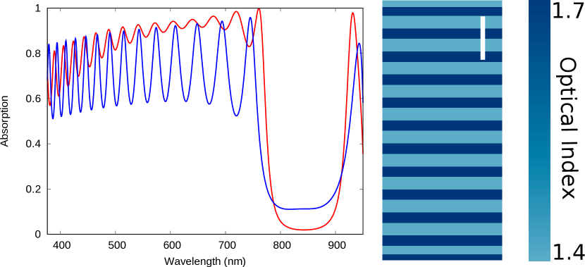
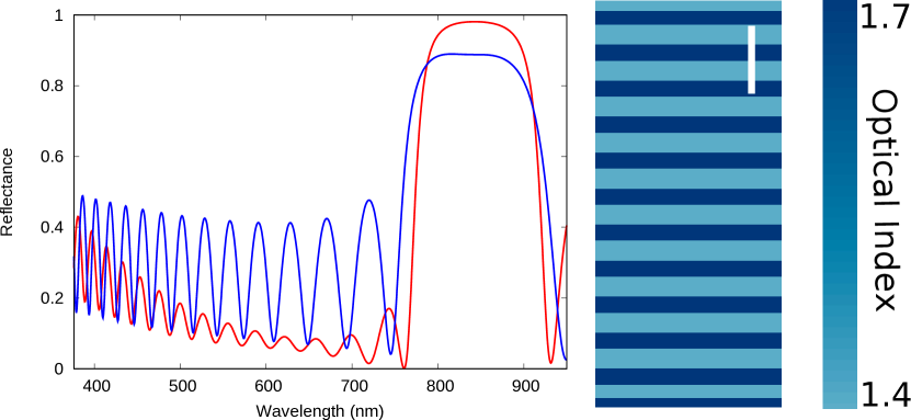
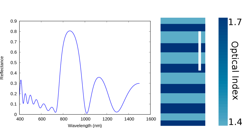
The structure which will serve as a reference in the following, and that we call the simplified ARC is constituted of a Bragg mirror with a forbidden band center at 835 nm, with two adapted layers on top of the structure (in contact with air) of 79 and 102 nm; and at the bottom (close to silicon) of 100 and 70 nm. The structure as well as its absorption spectrum are shown on Fig. 1, compared to the absorption spectrum of the photonic crystal alone. The role of the additional layers can be easily understood: they reduce the oscillations which can be seen in the spectrum and thus maximize the absorption in the visible range where the silicon is absorbent. The overall behavior of the structure is even better understood when looking at the reflectance of the structure, because the reduction of the oscillations and the high reflectance due to the forbidden band clearly appear on the spectrum Fig.2. This structure evokes Bragg mirrors equipped with ripple reduction layers, a classical technique used in optical filter synthesis for Bragg mirrors deposited on a glass substrate[14, 15, 16, 17]. Such a technique is however not used to generate anti-reflective coatings, as this is generally not the goal which is pursued.
In this part, we will discuss the optimally of the ARC structure, keeping in mind that it is generally impossible to prove that a solution provided by an optimization algorithm is actually optimal. Even worse, one should assume that an optimization almost never produces an optimal design. It is possible to build some confidence that a solution is close to being optimal when for instance (i) it is consistently obtained as a solution by the optimization algorithms (ii) a simple physical analysis allows to understand how the design operates. Here, we will couple a statistical analysis of the emergence of our solution to our physical understanding of this solution. We show that this kind of structure is not optimal, by providing slightly more efficient ARC for the largest index contrasts. However, as we show here, the fact the same structure emerges consistently reinforces our confidence that it is close to being optimal.
I.1 Methodology of the optimization
The cost function is the function which the algorithm will try to minimize. In our case, for a given multilayer structure characterized by the refractive index and thickness of each layer, we compute the short circuit current assuming an AM1.5 standard solar spectrum using the formula
| (1) |
where is the absorbance of the active layer, e, h and c are respectively the elementary charge, the Planck constant and the speed of light in vacuum and the spectral density of the illumination is given the solar spectrum[18]. We divide by the maximal theoretical short-circuit over the 375-750 nm range, . Since we want to maximize this quantity, the cost function is defined by
so that it is comprised between 0 and 1. Said otherwise, when the cost function is decreased by 0.1, this corresponds to an increase of the short-circuit current equal to 10% of the maximum achievable current.
We expect the problem we study to be modular, meaning that different regions of the structure will play almost independent roles, which is often the case for multilayered structures. In order to chose the right algorithm as well as the right variant and parameters for our problem, we have compared different algorithms and their variants on the most modular problem we have identified: the case of the high reflectance filter on a broad spectral range, leading to a chirped design[19]. On this problem, the evolutionary algorithm called Differential Evolution (DE) is the most efficient[10], but several variants of DE exist. After comparing the most common variants (DE/rand/1, DE/best/1, DE/randToBest/1, DE/currToBest/1, DE/rand/2, DE/best/2, identified according to the usual classification [20]) we have selected the DE/randToBest/1 variant. Finally, we have tuned the parameters of the algorithm so that it is finds the solution are quickly and as reliably as possible for the chirped dielectric mirror. We underline that this testbed is freely available in the Nevergrad library[21, 22].
We thus consider a population of 30 individuals chosen randomly. Each individual is a potential structure solution and is defined by a vector, corresponding to a location in what we call here the phase space. To generate a new generation, each individual is compared to a new individual. The parameters of the new individual come either directly from the current individual to be improved with a probability or from a mutant generated using the formula
| (2) |
where is the mutant, , and are the vectors which correspond to individuals chosen randomly in the population, while is the vector corresponding to the individual with the lower cost function. We have taken and . The cost function associated to the new individual is computed, and it replaces the current individual in the population only if it has a lower cost function.
We have put boundaries on all the parameters. Here we force the thicknesses of each layer to be comprised between 30 and 250 nm. When a new individual is generated using mutation, there is no guarantee that it will satisfy these conditions. When this is not the case for a parameter, it is simply replaced by the parameter of the current individual. This allows to explore correctly all the authorized phase space, without neglecting the edges – because the best solution is frequently found near these limits, especially when the refractive index vary[10]. We underline that in some of our optimizations, we left the refractive indexes of each layer vary. In those cases we performed a structured optimization by considering that the refractive index and the thickness of a layer constitute a single parameter: when a new individual is generated, either the two parameters are taken from the parent or they are computed using formula (2) with the same individuals. In general this drastically improves the efficiency of the algorithm[23], underlining once more what a physical understanding can bring to the optimization even a priori.
In order to estimate whether a solution is produced systematically or not, we run 50 times DE on each problem (with a given number of layers), making sure that each run has converged by allocating a large enough budget[24]. Then we plot all the different values of the cost function for the best individual obtained for each optimization, sorting them starting with the lowest as shown Fig. 3.
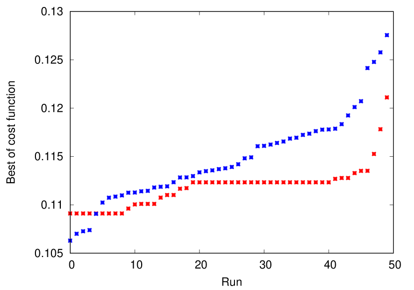
This kind of representation allows to estimate whether the solution was produced by pure luck or not. A plateau for the lowest value indicates that the solution is often found. A plateau at a different value indicates that there is another solution with a large attraction basin in the phase space which is often found by the algorithm (these two types of plateau can be seen Fig. 3).
Generally, for a multilayered optical filter, the higher the number of layers, the more efficient it is, and thus the lower the cost function [14, 3, 22, 10]. This unique property allows to better estimate when the algorithms struggle to find a solution by plotting the lowest cost function obtained for 50 run versus the number of layers of the structure. In general, this curves shows a smooth decline as the number of layers grows and then becomes chaotic – signaling that the results are no longer reliable because the problem is too complex for the algorithm.
I.2 Results
First we have run optimizations as described above, for an even number of layers ranging from 4 to 50, the structure beginning with the lower index (1.4) and ending with the higher (1.7). The structure is placed on top of an infinite hydrogenated amorphous silicon substrate. We have plotted Fig. 4 the best cost function obtained as a function of the number of layers. On the same figure, we have plotted the cost function obtained for our simplified ARC, described above.
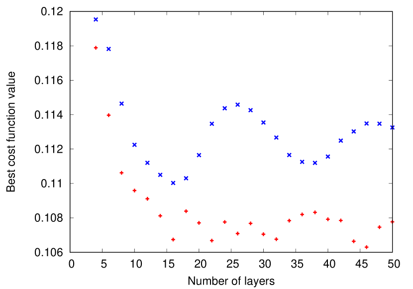
Changing the thickness of the photonic crystal inside the ARC amounts to shifting the oscillations which can be seen on its spectrum as shown Fig.2. As a result, the cost function of the simplified ARC presents quasi-periodic oscillations when the number of layers increases. The values of the cost function for the simplified ARC are just slightly larger than for the fully optimized structure. We consider this is a sign that small changes are brought by the algorithms to adapt even more the ARC, but that they will bring minor improvements only. The simplified ARC thus captures the main characteristics of the optimized structures. Furthermore, Fig. 4 indicates that even for 50 layers the optimization is reliable, since it always provides solutions that are better than the simplified ARC despite the increase in complexity of the problem.
Setting the refractive index of the layers, how they alternate, an even number of layers are arbitrary choices which may have introduced bias and may be responsible for the emergence of the structure. We have thus run optimizations for different cases[24] and almost each time, the optimized structure is a photonic crystal with the most of the time two adapted layers at each sides.
We represent the cost function values of the best structures obtained in the standard conditions as a function of the number of layers in the structure in red in Fig.4. We note that the structure with 12 layers is particularly efficient. Fig. 5 shows the structure and the corresponding reflectance spectrum. Fig. 3 shows that this 12 layers structure is obtained very consistently, since a plateau can be seen for the lowest values of the cost function.
I.3 Discussion
Our results clearly indicate that a Bragg mirror with adapted outer layers is an obvious strategy to reduce the reflection for a photovoltaic device. The design emerges systematically whatever the conditions. Even when the algorithm cannot be considered to produce a satisfactory solution (i.e. as efficient as the simplified ARC), the results point in that direction, obviously resembling the reference and presenting the same level of efficiency but never clearly outperforming it.
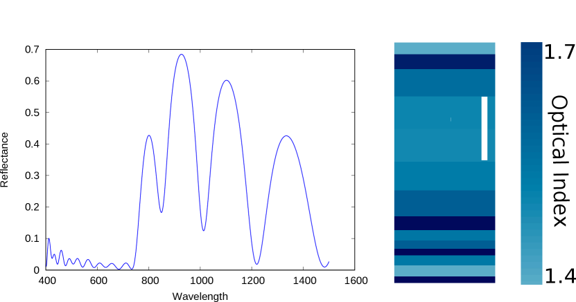
For a photovoltaic problem, extending over most of the visible spectrum and with a relatively bumpy AM1.5 illumination, a much more disordered structure could have been expected. In similar situations, engineered disorder has actually proven to be a very fruitful approach[25]. Even seemingly ordered structures which occur in nature, like that of the Morpho butterfly[10] do contain some kind of correlated disorder[25]. The structures we obtain do also, to better adapt to the AM1.5 spectrum obviously, but this remains limited – so that the ordered structure can always be distinguished. However, different structures may well emerge if the way the efficiency of the structure is assessed (and thus the cost function) changes. Figure 6 shows another ordered design, which emerges when the refractive index range is extended and the refractive index is let to vary. This structure can be deemed regular, with a striking symmetrical pattern at its core. However, the reasons why it emerges remain unclear: one would expect such a smooth refractive index profile to lead to some kind of localization of light inside the structure, a seldom desirable feature in this context. This shows anyway that while the range of situations where a periodic structure emerges is relatively broad, such a structure is not systematically the best solution.
Moreover, simulations show that when the incidence angle is modified, the photonic bandgap of the crystal is shifted towards shorter wavelengths, which is detrimental to the efficiency. A new cost function including a wide angular range may then lead to completely different structures, eventually disordered. The design we present may thus be optimal only in normal incidence.
We underline that the solutions to ARC problems in the literature, generally obtained using specific design algorithms[2, 3], are generally complex, but sometimes quite regular too[26] – so that the emergence of a periodic design is not new. However, the designs are still difficult to understand compared to the design we study here and which is definitely original.
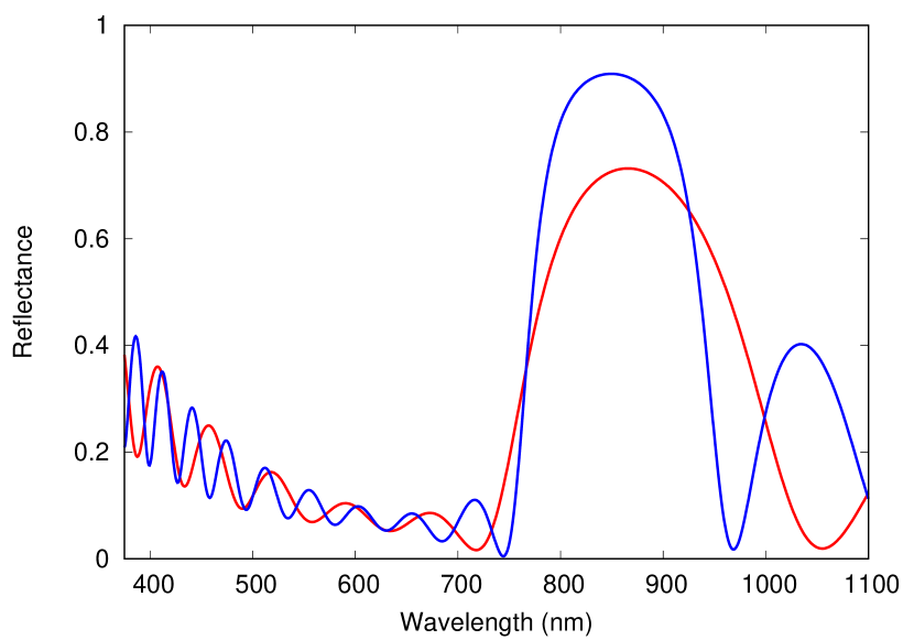
The strategy suggested here by the optimization is very similar to what is done for Bragg mirrors in order to reduce the so called ripples – the oscillations in the spectrum outside of the bandgap[15, 16, 17, 27, 28]. Such oscillations are commonly thought as produced by some kind of reflection inside the structure due to the ”mismatch between the structure and the surrounding media”[16]. The amplitude of the ripples is actually not modified whatever the number of layers of the photonic crystal, as shown Fig. 7. We have thus followed this idea by trying to retrieve the reflection coefficient of the Bloch mode inside the structure and to see how it is modified by the adapted layers.
II Physical analysis through a cavity model for the Bloch mode
Inspired by the results provided by the optimization, we study in this part our simplified ARC as described above.
Even though a Bragg mirror is actually considered by most authors as a slab in which a Bloch mode propagates and is reflected by both edges, there has been little work supporting such an idea because of the lack of any theoretical method to define or compute the reflection or transmission coefficients of the Bloch mode.
Here we show that such coefficients can be computed by using a cavity model to fit the actual data, allowing a thorough physical analysis of the whole structure.
II.1 Fabry-Perot cavity model
Inside an infinite Bragg mirror, light propagates as in an homogeneous medium under the form of a Bloch mode, which has the profile of a plane wave. Each Bloch mode is characterized by a wavevector along the direction of the interfaces and a wavevector perpendicularly to the interfaces noted here. In the following, the light is assumed to illuminate the structure in normal incidence, so that and the dispersion relation giving reduces to
| (3) |
with the period of the photonic crystal, the wavevector inside medium of refractive index and thickness , and .
In the bandgap of the Bragg mirror, is purely imaginary, which means that the Bloch mode will not propagate inside the structure. In the spectral range we consider, the wavevector will be assumed to be real and the Bloch mode propagative.
A Bragg mirror with a finite number of periods, with or without adapted outer layers will be considered here as a cavity for the Bloch mode defined above, with a wavevector given by the dispersion relation for the infinite Bragg mirror.
In the framework of such a model, the reflection coefficient of the whole structure with a Bragg mirror with a thickness is given by a cavity model
| (4) | |||
| (5) | |||
| (6) |
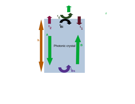
with and the upward and downward amplitudes of the Bloch mode, the reflection of the incident plane wave on the first layer of the photonic crystal, and the transmission coefficients between free space and the Bloch mode, (resp. ) is the reflection coefficient of the Bloch mode on the outer layers (resp. the substrate). The whole model with the different coefficients is summarized Fig. 8.
Those formula leads to Fabry-Perot formula for the reflection coefficient of the whole structure
| (7) |
II.2 Fit with a Fabry-Perot formula
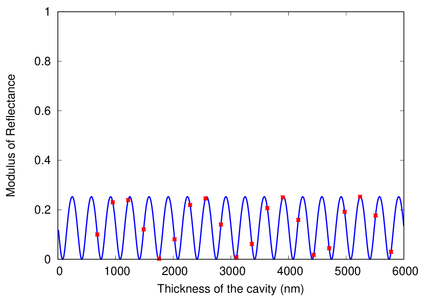
Retrieving the internal transmission and reflection coefficients of the model would be a relatively easy task if only it were possible to make the thickness of the structure take arbitrary values for a given frequency. However, the core of the structure has a thickness which is always a multiple of the period of the crystal . The problem is illustrated Fig. 9 where the red point indicate the available data, as well as a reliable fit with a periodicity imposed by the Bloch mode wavevector. Retrieving the internal coefficients is thus non trivial and requires a purely numerical approach.
To summarize, we fit the data with a cavity model. However, given the structure of the formula, it is not possible with a single fit to determine all the internal coefficients. The model for the reflectance which we actually use is given by
| (8) |
where , and are the coefficients which can actually be retrieved, is given by the dispersion relation ((3)) and is the number of periods of the photonic crystal considered. In order to perform the fit, a rather complicated optimization process, we use DE again, and the cost function, defined for a given frequency by
| (9) |
where is the reflection coefficient of the whole structure, computed using an impedance formalism[14] to reduce the computational cost. A single optimization run is usually enough to determine satisfactory coefficients, as shown Fig. 9. It is striking how the periodicity of the model, imposed by the wavevector calculated independently of the fit, is different from the apparent periodicity of the data. This illustrate why the fitting process is difficult.
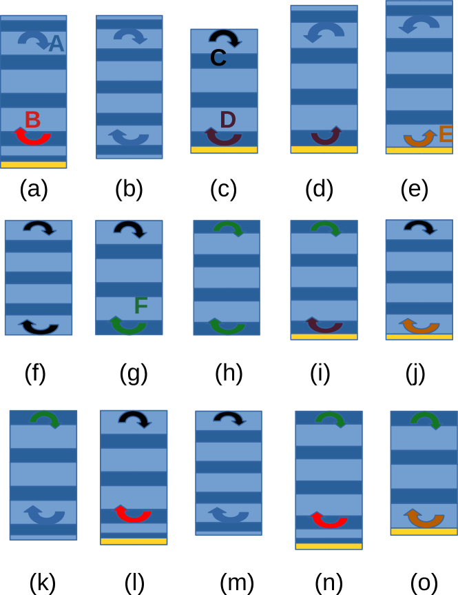
We can find the coefficient by using the fitting process. However, it provides an immediate access to the internal reflection coefficients only in the case of a symmetric structure. In general, is the product and thus the determination of both coefficients is not straightforward. We prove[24] that determining these coefficients is possible and constitutes a coherent approach, provided the fitting process is applied to a variety of symmetric and asymmetric structures (see Fig.10).
We have check for all the structures shown Fig. 10 that our approach produces perfectly coherent results, allowing us to access the reflection coefficient of the Bloch mode whatever the termination for the Bragg mirror considered (abrupt or adapted, with silicon or with air).
II.3 Discussion
Now that we have access to the reflection coefficient of the Bloch mode, we can compare the response of the structure when the Bragg mirror is terminated abruptly and when the adapted layers are added.
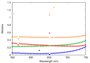
Fig. 11 shows the comparison between the internal reflection coefficient with abrupt or adapted termination, whether on the side of air or of silicon. In both cases the role of the adapted layers appears very clearly: the modulus of the reflection coefficient is significantly reduced. This is particularly striking for the layers between the Bragg mirror and air. This strengthen the idea of that the adapted layers allow to reduce the mismatch between air and the Bragg mirror, reducing the internal reflection coefficient and finally the ripples.
The Bragg mirror can finally be considered as a buffer in the structure generated by the algorithms. It is difficult to reduce the impedance mismatch between air and silicon, because this mismatch is really large. Anti-reflective coatings with gradually increasing refractive index can be very efficient, but such structures require a wide range of available refractive index, typically ranging from 1 to the at least 3 (close to the refractive index of silicon)[29]. The Bragg mirror with adapted terminations emerges because, with a limited range of refractive index, a better solution is to minimize the mismatch between free space and the photonic crystal, and then between the photonic crystal and silicon. The role of the Bragg mirror is thus clearly to support the Bloch mode, characterized by an effective index, and to serve as a buffer. That is the reason why, when the number of layers is increased, the algorithms tend simply to add periods to the Bragg mirror.
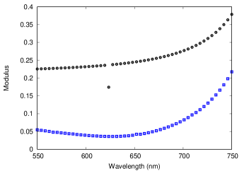
This interpretation is reinforced when the coefficient, the reflection coefficient of the incoming light on structure with an infinite Bragg mirror layer, which can be deduced from our optimizations, is considered. If we compare the coefficient obtained for structures without adapted layers, we see a reduction of by a factor of 4 to 5 typically when adapted layers are added (see Fig. 12), which is completely coherent with the idea of a reduced impedance mismatch between air and the photonic crystal.
III Fabrication and characterization of the anti-reflective coating
Finally, we have checked that the designs suggested by optimization could be easily fabricated while relying on a technique which could potentially be deployed on currently existing production lines. We have used a reactive sputtering, a process which is known to be easily scalable, to fabricate non-stoechiometric silicon oxynitride layers whose refractive index range typically from 1.4 to 1.7. Higher index can be reached for a higher content in silicon with this technique[11], however in that case the layers become absorbent. A crystalline silicon target is placed at 9.5 cm in front of a rotating substrate holder and sputtered using a radiofrequency power of 250 W and at 13.56 MHz in an atmosphere of [11]. The gas flows and are controlled using mass flowmeters. In the present work, the flows of and are put at a fixed value, while the flow of was made to vary periodically. More precisely, we use a a rectangular pulsed flow rate from 0 during the off-time , to a maximum flow rate during the on-time . Depending on pulsed parameters (, and ), time-averaged flow rate is tuned during target sputtering which gives us a precise control on the composition of the deposited film, e.g. x, y and z in material and so on their refractive index.
Two samples have been fabricated, corresponding to structures with a relatively low number of layers. The results presented above show that the physical mechanism which explain the efficiency of the ARC can actually occurs for as few as 6 layers, with only one period of the photonic crystal. The second sample corresponds to two periods of the Bragg mirror and thus 8 layers. These two structures are potentially cheap to manufacture and thus are more likely to be deployed some day than coatings with a thicker photonic crystal.
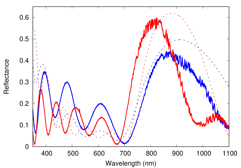
We measure the reflectance of the fabricated structures at room temperature. A halogen lamp is used as a visible light source. The collimated light is directed on the sample, then the reflected signal is focused on the monochromator slits entrance. A 32 cm focal monochromator coupled with a CCD camera is used as the detection.
The measured spectra obtained for the two samples shown Fig. 13 are in relatively good agreement with theoretical calculations, showing both a part of the spectrum presenting a low reflectance and a higher reflectance in the gap of the photonic crystal. We have little doubt that imperfections in the fabrication process, which is far from being optimized yet, are responsible for the discrepancies. At least, these results show how easily the ARC we have designed can be fabricated with easily deployable techniques.
IV Conclusion
We shown that evolutionary optimization of anti-reflective coatings for photovoltaic devices systematically yields photonic crystals with adapted terminations. While such structures may not be perfectly optimal, we have established that they emerge for a very broad set of conditions. Such solutions can be called robust. While such an approach reminds of ripple reduction strategies which have been known for a very long time[16], our work suggest that this class of structure should be the subject of much more attention. We insist that devices including photonic crystals whose working point is outside of the forbidden band, like the ARC studied here, are finally not that common[30].
Light propagates in photonic crystals under the form of Bloch modes. Since their invention, Bragg mirrors have been thought as cavities for such a mode, and the ripples outside of the photonic bandgap as a signature of slab resonances. We have proposed a methodology to retrieve the internal reflection coefficient of the Bloch mode – quantities which can not be retrieved analytically. First, our analysis is in complete agreement with the picture of finite structures as cavities. Second, our approach has confirmed that the outer layers of our ARC reduce the impedance mismatch between the outside media and the photonic crystal. The periodic part of the structures can thus be thought of as a buffer for light.
This strategy is robust, in the sense that only the outer layers have to change when either the outer media or the index contrast change, explaining why such structures emerge so easily as solutions. Here, the physical analysis strengthens the confidence we have in the optimization process. A physical analysis is a powerful tool allowing to easily guess that a structure is probably sub-optimal or to perceive more precisely why it emerges[10] and even to guide an optimization[31, 32]. As a consequence, we think the result of an optimization should always be discussed physically, which is only seldom done[33, 34].
Finally, we have shown that these structures can be easily fabricated using a sputtering process which is increasingly used in the industry. We underline that the bandgap of the photonic crystal present in our designs has the potential to reduce the heating of a potential solar cell, as it would reflect a part of the infra-red spectrum which is not always able to generate electron-hole pairs. This could be a real advantage for some photovoltaic devices when performances are more important than costs, like for concentration photovoltaics for instance[35].
We underline that we have been able to physically understand the structures produced by optimization because they are regular. In addition to being often a sign that the structure is close to optimality[33, 10, 26], regularity generally allows for a physical analysis and thus, for the results of the optimization to be used as a true source of inspiration. As very few algorithms have in the past yield regular structures, the present work is one of the first example of such an a posteriori analysis. This is welcome because bio-inspiration does not always offer relevant solutions to technological problems, particularly in photonics. Being able to generate photonic structures which are technologically relevant through an evolution-like optimization process may be more promising.
V Acknowledgments
The authors would like to thank Théo Charreyron for his help. Computations have been performed on the supercomputer facilities of the Mésocentre Clermont Auvergne University. Antoine Moreau is an Academy CAP 20-25 chair holder. He acknowledges the support received from the Agence Nationale de la Recherche of the French government through the program “Investissements d’Avenir” (16-IDEX-0001 CAP 20-25).
References
- Piggott et al. [2015] A. Y. Piggott, J. Lu, K. G. Lagoudakis, J. Petykiewicz, T. M. Babinec, and J. Vučković, Inverse design and demonstration of a compact and broadband on-chip wavelength demultiplexer, Nature Photonics 9, 374 (2015).
- Tikhonravov and Trubetskov [1994] A. V. Tikhonravov and M. K. Trubetskov, Development of the needle optimization technique and new features of OptiLayer design software, in Optical Interference Coatings, Vol. 2253, edited by F. Abeles, International Society for Optics and Photonics (SPIE, 1994) pp. 10 – 20.
- Tikhonravov et al. [1996] A. Tikhonravov, M. Trubetskov, and G. DeBell, Application of the needle optimization technique to the design of optical coatings, Applied optics 35, 5493 (1996).
- Molesky et al. [2018] S. Molesky, Z. Lin, A. Y. Piggott, W. Jin, J. Vucković, and A. W. Rodriguez, Inverse design in nanophotonics, Nature Photonics 12, 659 (2018).
- Potyrailo et al. [2007] R. A. Potyrailo, H. Ghiradella, A. Vertiatchikh, K. Dovidenko, J. R. Cournoyer, and E. Olson, Morpho butterfly wing scales demonstrate highly selective vapour response, Nature Photonics 1, 123 (2007).
- Kinoshita et al. [2008] S. Kinoshita, S. Yoshioka, and J. Miyazaki, Physics of structural colors, Reports on Progress in Physics 71, 076401 (2008).
- Moreau et al. [2006] A. Moreau, O. Teytaud, and J.-P. Bertoglio, Optimal estimation for large-eddy simulation of turbulence and application to the analysis of subgrid models, Physics of fluids 18, 105101 (2006).
- Yu et al. [2020a] S. Yu, X. Piao, and N. Park, Machine learning identifies scale-free properties in disordered materials, Nature communications 11, 1 (2020a).
- Liu et al. [2018] J. Liu, A. T. Gaynor, S. Chen, Z. Kang, K. Suresh, A. Takezawa, L. Li, J. Kato, J. Tang, C. C. Wang, et al., Current and future trends in topology optimization for additive manufacturing, Structural and Multidisciplinary Optimization 57, 2457 (2018).
- Barry et al. [2020] M. Barry, V. Berthier, B. Wilts, M.-C. Cambourieux, P. Bennet, R. Pollès, O. Teytaud, E. Centeno, N. Biais, and A. Moreau, Evolutionary algorithms converge towards evolved biological photonic structures, Scientific Reports 10, 12024 (2020).
- Farhaoui et al. [2016] A. Farhaoui, A. Bousquet, R. Smaali, A. Moreau, E. Centeno, J. Cellier, C. Bernard, R. Rapegno, F. Réveret, and E. Tomasella, Reactive gas pulsing sputtering process, a promising technique to elaborate silicon oxynitride multilayer nanometric antireflective coatings, Journal of Physics D: Applied Physics 50, 015306 (2016).
- Parker et al. [2001] A. R. Parker, R. C. McPhedran, D. R. McKenzie, L. C. Botten, and N. Nicorovici, Aphrodite’s iridescence, Nature 409, 36 (2001).
- Defrance et al. [2016] J. Defrance, C. Lemaître, R. Ajib, J. Benedicto, E. Mallet, R. Pollès, J.-P. Plumey, M. Mihailovic, E. Centeno, C. Ciracì, D. Smith, and A. Moreau, Moosh: A numerical swiss army knife for the optics of multilayers in octave/matlab, Journal of Open Research Software 4 (2016).
- Macleod [2001] H. A. Macleod, Thin-film optical filters (CRC press, 2001).
- Macleod [2012a] A. Macleod, The quarterwave stack: 1 early history, Bulletin, Society of Vacuum Coaters, Issue Summer , 22 (2012a).
- Macleod [2012b] A. Macleod, The quarterwave stack: 2 properties, Bulletin, Society of Vacuum Coaters, Issue Fall , 16 (2012b).
- Macleod [2013] A. Macleod, The quarterwave stack: 3 a building block, Bulletin, Society of Vacuum Coaters, Issue Spring , 22 (2013).
- Santbergen et al. [2010] R. Santbergen, J. Goud, M. Zeman, J. van Roosmalen, and R. C. van Zolingen, The am1. 5 absorption factor of thin-film solar cells, Solar energy materials and solar cells 94, 715 (2010).
- Szipőcs and Kőházi-Kis [1997] R. Szipőcs and A. Kőházi-Kis, Theory and design of chirped dielectric laser mirrors, Applied Physics B: Lasers and Optics 65, 115 (1997).
- Storn and Price [1997] R. Storn and K. Price, Differential evolution: A simple and efficient heuristic for global optimization over continuous spaces, J. of Global Optimization 11, 341 (1997).
- Rapin and Teytaud [2018] J. Rapin and O. Teytaud, Nevergrad - A gradient-free optimization platform, https://GitHub.com/FacebookResearch/Nevergrad (2018).
- Bennet et al. [2020] P. Bennet, E. Centeno, J. Rapin, O. Teytaud, and A. Moreau, The photonics and ARCoating testbeds in Nevergrad (2020), working paper or preprint.
- Rapin et al. [2020] J. Rapin, P. Bennet, E. Centeno, D. Haziza, A. Moreau, and O. Teytaud, Open source evolutionary structured optimization, in Proceedings of the 2020 Genetic and Evolutionary Computation Conference Companion (2020) pp. 1599–1607.
- [24] See Supplemental Material at http://link.aps.org/supplemental/10.1103/PhysRevB.103.125135 (or below) for supplementary figures and a more detailed discussion about the emergence of the design and the retrieval of cavity model parameters.
- Yu et al. [2020b] S. Yu, C.-W. Qiu, Y. Chong, S. Torquato, and N. Park, Engineered disorder in photonics, Nature Reviews Materials , 1 (2020b).
- Tikhonravov et al. [2008] A. V. Tikhonravov, M. K. Trubetskov, T. V. Amotchkina, and J. Dobrowolski, Estimation of the average residual reflectance of broadband antireflection coatings, Applied optics 47, C124 (2008).
- Thelen [1966] A. Thelen, Equivalent layers in multilayer filters, J. Opt. Soc. Am. 56, 1533 (1966).
- Thelen [1971] A. Thelen, Design of optical minus filters, J. Opt. Soc. Am. 61, 365 (1971).
- Centeno et al. [2019] E. Centeno, A. Farahoui, R. Smaali, A. Bousquet, F. Réveret, O. Teytaud, and A. Moreau, Ultra thin anti-reflective coatings designed using differential evolution (2019), arXiv:1904.02907 [physics.optics] .
- Centeno and Cassagne [2005] E. Centeno and D. Cassagne, Graded photonic crystals, Optics letters 30, 2278 (2005).
- Moreau et al. [2007] A. Moreau, C. Lafarge, N. Laurent, K. Edee, and G. Granet, Enhanced transmission of slit arrays in an extremely thin metallic film, Journal of Optics A: Pure and Applied Optics 9, 165 (2007).
- Moreau et al. [2012] A. Moreau, R. Smaali, E. Centeno, and C. Seassal, Optically optimal wavelength-scale patterned ito/zno composite coatings for thin film solar cells, Journal of Applied Physics 111, 083102 (2012).
- Gondarenko et al. [2006] A. Gondarenko, S. Preble, J. Robinson, L. Chen, H. Lipson, and M. Lipson, Spontaneous emergence of periodic patterns in a biologically inspired simulation of photonic structures, Physical review letters 96, 143904 (2006).
- Frellsen et al. [2016] L. F. Frellsen, Y. Ding, O. Sigmund, and L. H. Frandsen, Topology optimized mode multiplexing in silicon-on-insulator photonic wire waveguides, Optics express 24, 16866 (2016).
- Xing et al. [2015] Y. Xing, P. Han, S. Wang, P. Liang, S. Lou, Y. Zhang, S. Hu, H. Zhu, C. Zhao, and Y. Mi, A review of concentrator silicon solar cells, Renewable and Sustainable Energy Reviews 51, 1697 (2015).