The quantum efficiency and diffractive image artifacts of Si:As IBC mid-IR detector arrays at 5 10 m: Implications for the JWST/MIRI detectors
Abstract
Arsenic doped back illuminated blocked impurity band (BIBIB) silicon detectors have advanced near and mid-IR astronomy for over thirty years; they have high quantum efficiency (QE), especially at wavelengths longer than 10 , and a large spectral range. Their radiation hardness is also an asset for space based instruments. Three examples of Si:As BIBIB arrays are used in the Mid-InfraRed Instrument (MIRI) of the James Webb Space Telescope (JWST), observing between 5 and 28 . In this paper, we analyze the parameters leading to high quantum efficiency (up to 60%) for the MIRI devices between 5 and 10 m. We also model the cross-shaped artifact that was first noticed in the 5.7 and 7.8 Spitzer/IRAC images and has since also been imaged at shorter wavelength () laboratory tests of the MIRI detectors. The artifact is a result of internal reflective diffraction off the pixel-defining metallic contacts to the readout detector circuit. The low absorption in the arrays at the shorter wavelengths enables photons diffracted to wide angles to cross the detectors and substrates multiple times. This is related to similar behavior in other back illuminated solid-state detectors with poor absorption, such as conventional CCDs operating near 1 m. We investigate the properties of the artifact and its dependence on the detector architecture with a quantum-electrodynamic (QED) model of the probabilities of various photon paths. Knowledge of the artifact properties will be especially important for observations with the MIRI LRS and MRS spectroscopic modes.
1 Introduction
Developed in the 1980’s (e.g., Petroff & Stapelbroek, 1980, 1984, 1985; Stetson et al., 1986), arsenic doped extrinsic silicon (Si:As) Blocked-Impurity-Band (BIB - or Impurity Band Conductor - IBC) detector arrays are widely used in the field of mid-infrared astronomy. Multiple space missions have made them their detector of choice due to particular attributes: their wide spectral region coverage (5-28 m), high quantum efficiency, low dark current, stable performance for an extended period of time, low heat dissipation (which is particularly important for cryo-cooled space missions), and nuclear radiation hardness. The sizes and performance of arrays of these detectors have increased over time. The Short Wavelength Spectrometer on the Infrared Satellite Observatory (ISO), launched in 1995, utilized a 1 12 array (Leech et al., 2003), the MSX satellite, launched in 1996, had 8 192 arrays (Mill et al., 1994), while IRS and MIPS on the Spitzer Space Telescope had 128 128 devices (Van Cleve et al., 1995) and the IRAC/Spitzer 5.7 and 7.8 m (Hora et al., 2004) and the Akari (Onaka et al., 2007) arrays were 256 256. The latest generation detectors are 1024 1024, such as the 12 and 23 m arrays of the WISE mission (Mainzer et al., 2008) and the three focal plane arrays (FPAs) (Ressler et al., 2008) mounted in the Mid-InfraRed Instrument (MIRI) of the James Webb Space Telescope (JWST).
Much of the theory on the operation of these detectors was published in the 1980’s, shortly after they were invented, i.e.: Petroff & Stapelbroek (1984, 1985); Stetson et al. (1986); Szmulowicz & Madarsz (1987); Szmulowicz et al. (1988). Since then there has been substantial progress in the detector quality, primarily through improved control of minority impurities, resulting in successful fabrication of devices with much thicker infrared-active layers than previously (Love et al., 2004). The original efforts are largely successful in describing the properties of these improved devices at the longer wavelengths. However, testing of detectors with these thicker layers showed that the behavior of responsivity vs. bias voltage requires introduction of a diffusion length of 2.5 m (rather than the negligible diffusion length in the original theory), or the response at low bias and wavelengths near the peak of response would fall short of measurements (Rieke et al., 2015). This change is required because at wavelengths 15 m, most of the photons are absorbed in the first 10 microns of the infrared-active layer. At low bias, the field does not penetrate across this layer and the photo-electrons must diffuse across a field-free zone to be collected and produce a signal.
In addition, the detectors have been utilized down to wavelengths as short as 5 m, far from their peak response at 12 - 25 m. Quantum Efficiencies (QE)111QE is defined as the fraction or percentage of incident photons converted to electrons of 40% are expected in the 5 - 8 m range (Love et al., 2005; Woods et al., 2011). Such applications complement InSb and HgCdTe photodiodes that until recently have had high performance only at wavelengths short of 5 m. Most notable of these applications was the IRAC/Spitzer channel 3 and 4 detector arrays (Fazio et al., 2004; Hora et al., 2004), developed by Raytheon (Estrada et al., 1998). Pre-launch measurements indicated that the IRAC detectors reached a QE of 37% (following revisions after launch) and 56% at 5.6 and 8.0 m, respectively (Pipher et al., 2004). However, on orbit the achieved performance fell short of expectations from these values; the equivalent instrument throughputs were only 45% and 61% of the pre-launch predictions, respectively. This discrepancy was traced to a substantial portion of the signal appearing over an extended region on the detector. This signal was included in the laboratory measurements that integrated over a large fraction of the array, but was excluded in the on-orbit measurements, which were analyzed with point-source photometry (Hora et al., 2004). This behavior raises a question about whether the expected QE was actually achieved.
On-orbit images with IRAC showed that this extended response appeared as an image artifact, which the IRAC publications termed “banding” (Hora et al., 2004; Pipher et al., 2004). The artifact can be described as a cross along the pixel columns and rows centered on the sources. Various tests were executed on a sister detector of the IRAC flight hardware at the University of Rochester to find the origin of the artifact (Pipher et al., 2004). External optical effects were ruled out by the placement of a dark mask around the laboratory pinhole, which did not mitigate the “banding.” Their tests also showed that the strength of the artifact increases with decreasing wavelength and that light is scattered not just into the bands, but also into the entire detector area. These results indicate that the artifact is not due to an issue with the readout electronics but is internal to the detector. The IRAC Instrument handbook (Laine, 2015) describes the banding as a result of diffraction off the rectilinear grid of conductive pads and multiple scattering within the detector. This conclusion indicates that the behavior is similar to scattering observed in the near infrared with conventional CCDs (Gull et al., 2003; Ryon, 2019); i.e., that it is a general issue with back-illuminated solid state detectors being operated in spectral regimes where they have poor absorption.
This paper complements the evaluation of the long wavelength behavior of Si:As IBC detectors described in Rieke et al. (2015). We will discuss both the short wavelength QE and the imaging artifacts. We start with a description of the detector architecture (Section 2). We then derive the wavelength dependence of the quantum efficiency and show good agreement with the behavior of the flight detectors for MIRI on JWST, including quantum efficiencies of up to 60% in the 5 10 m range for arrays with suitable anti-reflection coatings (Section 3). The remainder of the paper focuses on the cause and morphology of the spreading of images in the shorter wavelengths, i.e., the “banding,” or the more descriptive term “the cross artifact” (Section 4). The work and modeling in this paper will inform the on-orbit image analysis for MIRI, which will in turn be used to refine the models to enhance the calibration of this instrument, particularly of its spectrometers.
2 Detector architecture
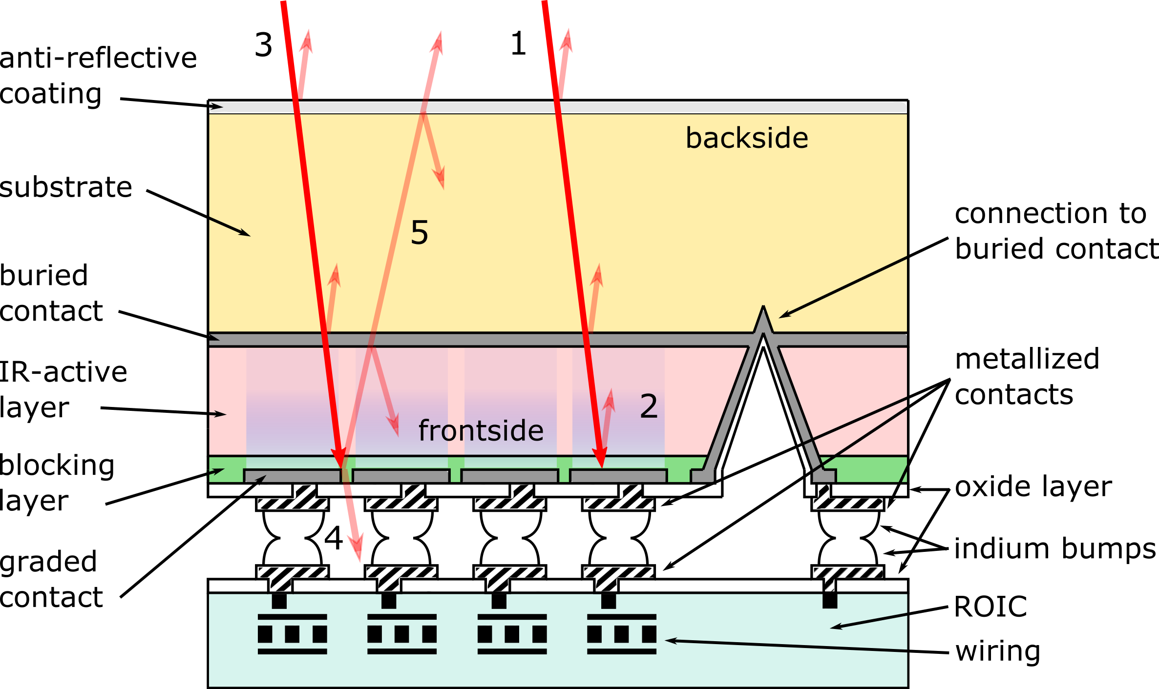
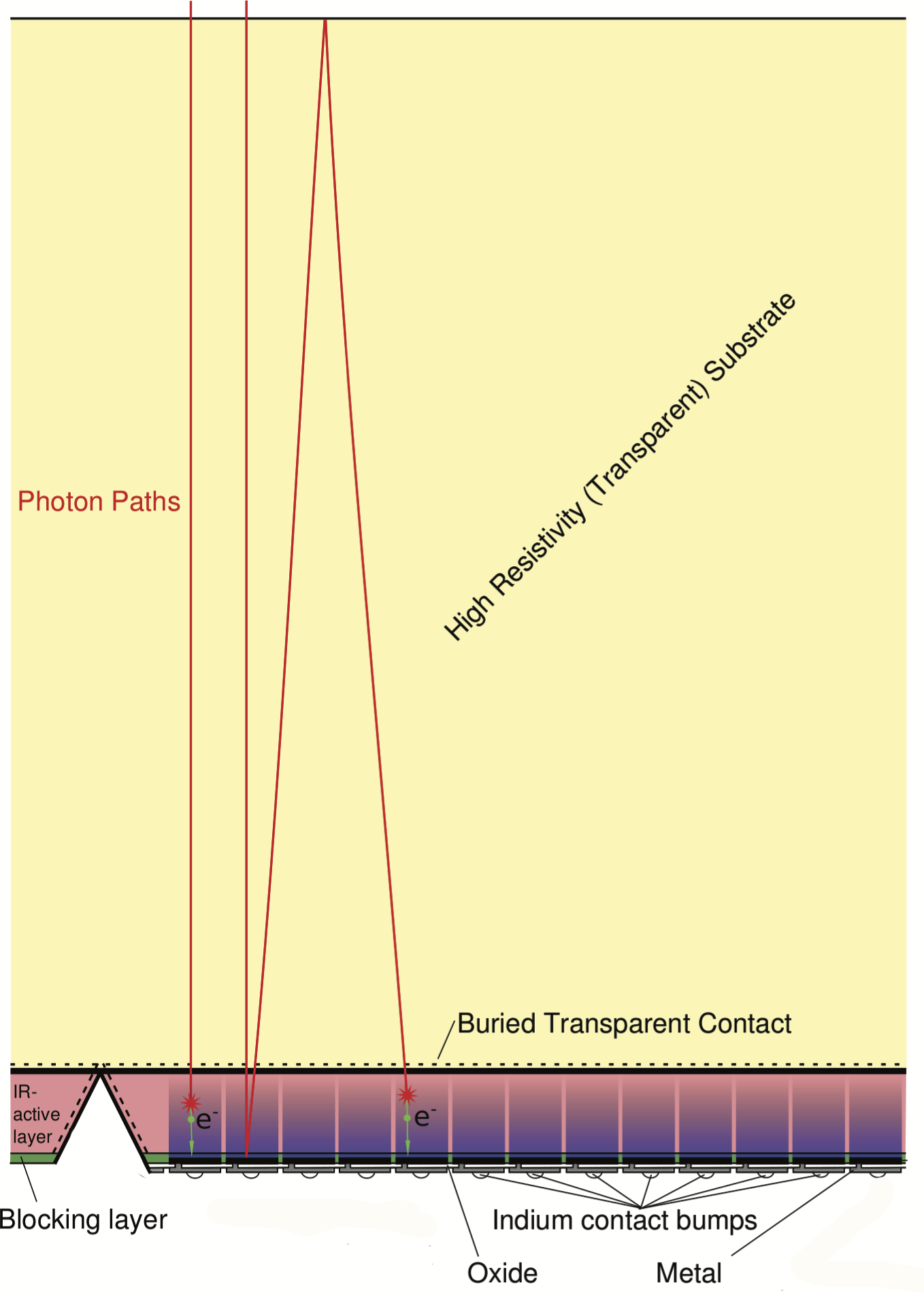
In Figure 1, we show the general architecture of modern Si:As IBC detector arrays. The detectors are grown on a substrate and illuminated through it. They consist of (1) a buried contact to establish an electrical field, (2) an IR-active layer that is heavily doped with arsenic to create an impurity band where the photons are absorbed, elevating free electrons into the conduction band, (3) a high purity layer that blocks dark current from the impurity band but allows passage of photoelectrons in the conduction band, and (4) an output contact. For the MIRI baseline arrays, the substrate is 420 m thick, the IR-active layer is 35 m, and the blocking layer is 4 m. The substrate is of a high resistivity (i.e., low impurity content) silicon wafer. The arsenic impurity (a donor) in the IR-active layer has a concentration of cm-3, while acceptor-type impurities are at a level of about cm-3. This low level of the minority impurity is critical to allow the electric field (shown in blue shading in the figure) to penetrate the IR-active layer for complete collection of photoelectrons at a bias level that does not trigger avalanche gain (and the resulting increase in noise). The 4 m thick blocking layer just before the output contacts is of high purity and hence has no impurity band. As a result, it blocks thermal currents, while allowing free transit to photoelectrons, which have been elevated into the conduction band (which, of course, is continuous from the IR-active layer through the blocking one). When the photoelectrons reach the contacts, they are sensed by integrating amplifiers in the readout integrated circuit (ROIC), connected through indium bump bonding hybridization (i.e., cold welding of indium bumps deposited on the detector and the readout wafers).
Figure 1 also illustrates some fates for incident photons. There are reflective losses at the entrance to the substrate and both reflective and absorptive ones in the buried contact. Near the peak of response (12 - 24 m) close to all the photons that survive through these layers are absorbed in the IR-active layer, either in the first pass (downward in Figure 1) or after reflection from a metallized contact. However, a significant fraction of photons () that are not absorbed in the initial downward pass are lost within an inter-pixel gap, while others undergo diffraction due to the pixel lattice structure (the fraction of photons that diffract depends on the detector architecture and the wavelength of the photons). In the region of peak response, very few of these photons will get through the IR-active layer on their upward trajectory and are therefore most likely detected in the same pixel as they entered. However, if the IR-active layer has low absorption many of them will escape back upward into the substrate. Many of those will be sufficiently off-normal to undergo total internal reflection when they encounter the upper edge of the substrate, leading to their being trapped in the silicon. These photons are responsible for the large scale of the imaging artifact.
3 Response and quantum efficiency
Si:As IBC detectors can offer systems level advantages through their ability to provide good performance from 5 through 27 m. To quantify this performance, in this section we consider the QE and response in the 5 10 m range, where the arsenic absorption coefficient is less than the values at the peak of response from 12 20 m. The low values of the absorption cross section between 5 and 10 m have led to a presumption that the QE of the detectors would be low there. However, QEs of up to 60% are achieved by the MIRI detectors; our model explores the parameters that make such high levels possible.
3.1 Modeling the response
Our model of the short wavelength response of Si:As IBC detectors uses the parameters of the MIRI “baseline” devices as described above and in more detail by Love et al. (2004, 2005, 2006); Ressler et al. (2008); Rieke et al. (2015); Ressler et al. (2015). We assume that the wavelength-dependent response is determined through a combination of (1) the absorption characteristics of the Si:As, (2) the anti-reflection coating on the entrance surface, (3) the optical characteristics of the buried contact, and (4) geometric factors.
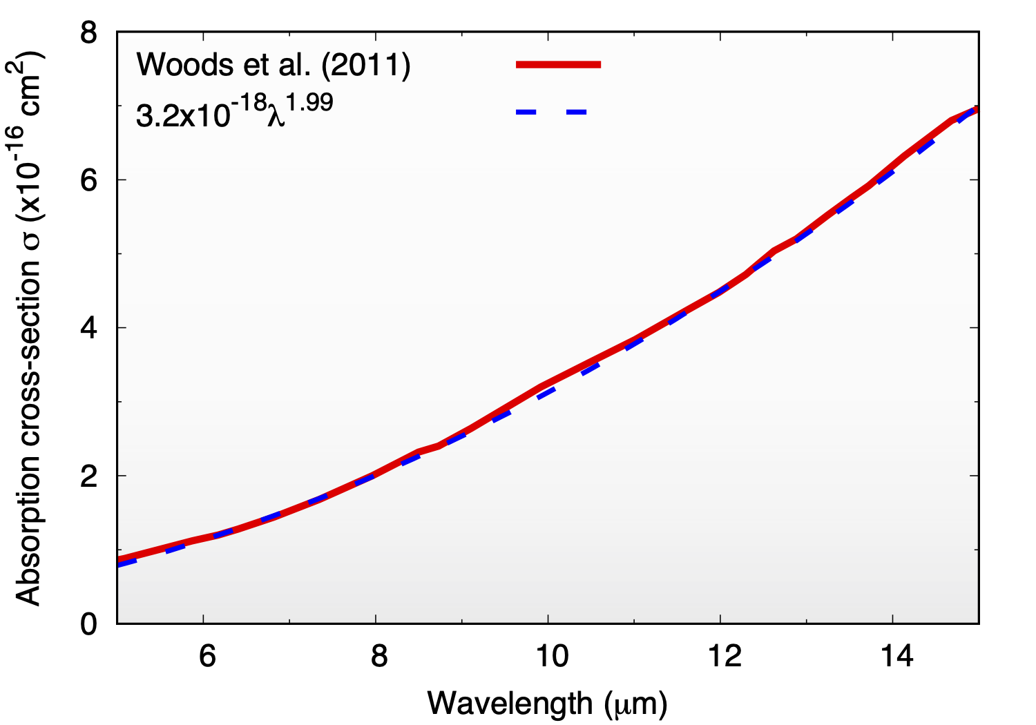
There are a number of determinations of the absorption cross section of As in Si (Petroff & Stapelbroek, 1985; Geist, 1989; Woods et al., 2011). Geist (1989) shows that taking the cross section to be 0.7 times the formula provided by Petroff & Stapelbroek (1985) provides an excellent fit to the data between 500 and 750 cm-1 (13.3 – 20 m). The Petroff & Stapelbroek (1985) fit follows a dependence of between 5 and 25 m. However, Geist (1989) finds that the slope in the theoretical study of Coon & Karunasiri (1986) is steeper, as . The measurements of Woods et al. (2011) are the only ones extending down to 5 m (and below). They agree with those of Geist (1989) and Petroff & Stapelbroek (1985) in most of the region of overlap. They are inaccurate beyond 25 m, failing to reflect the steep drop in sensitivity that begins at 27 m. However, the region from 5 – 15 m is the range of interest for this paper. We show their results for these wavelengths in Figure 2 along with a fit proportional to .
Ilaiwi & Tomak (1990) show that the shape of the theoretically predicted absorption coefficient depends critically on the assumed potential describing the screening behavior of the impurities. However, their calculations agree very well with each other for the isotropic hydrogenic, Yukawa, and Hülthén potentials, all of which also agree with the behavior.
We consider the absorption coefficient to be well determined, therefore; to be specific, we have used the values from Woods et al. (2011). The errors on these values are estimated at 6% at 10 m but much larger at 2 m; we have assumed between 5 and 10 m they scale linearly, so they are 12% at the former wavelength.
The MIRI arrays have one of two single-layer AR coatings of ZnS, in one case optimized for 6 m and in the other for 16 m. We have modeled the array where this coating is optimized for 16 m, since the high absorption coefficient around this wavelength allows us to determine the effects of the buried contact unambiguously. We have taken cryogenic refractive indices for silicon from Li (1980) and for ZnS from Hawkins & Hunneman (2004). The predicted wavelength-dependent quantum efficiency shows two peaks, i.e., one at 16.3 m corresponding to and another at 5.8 m for (the wavelengths do not differ by exactly a factor of three because of the wavelength dependence of the refractive indices). These values are a result of tuning the modeled thickness of the AR coating to provide the best match to the observed peaks, deriving a value of 1.95 m (in good agreement with the measured value).
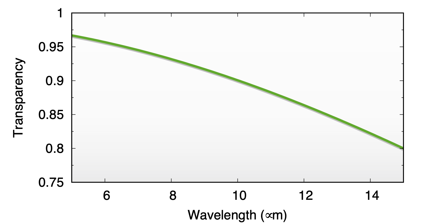
From early-on, it was recognized that the buried “transparent” contact was not fully transparent; Petroff & Stapelbroek (1985) estimated that it was 25% absorptive for one of their back-illuminated detectors. These contacts consist of a layer doped with a shallow impurity, such as arsenic, antimony, or phosphorus, so they show a decrease in absorption toward short wavelengths, just as photoconductive detectors based on such impurities do. The optical behavior of such contacts has been modeled by Hoelzlein et al. (1980) but is seldom included in modeling detectors. These models show that they both reflect and absorb incoming energy. We have obtained the absorptive component for typical contacts from M. G. Stapelbroek (private communication, see Figure 3). The fringing model described by Argyriou et al. (2020) indicates reflection at the level of 4% from 5 to 9 m (beyond 9 m, the detector absorption dominates the optical behavior). We have assumed 4% reflection at all wavelengths for the QE modeling (we ignore reflectance for the diffraction pattern modeling in the later part of the paper).
The primary geometric property affecting the detector quantum efficiency is the inter-pixel gaps in the backside contacts. The pixels are 25 m square and have pixel-to-pixel gaps of 2 m. The model described below assumes that all photoelectrons freed in the infrared-active layer are collected at a contact because of the fringing effect on electric fields for closely spaced electrodes (e.g. Lisowski & Skopec, 2009). However, photons that penetrate to the contacts are reflected back through the detector layer, where additional absorption adds to the photo-current. In our model, the reflected signal is decreased to match the areal coverage of the contacts. A small additional absorption occurs for photons reflected back from the buried contact or detector backside when they pass through the IR-active layer. The model will include a total of two complete passes through the detector (i.e. four passes through the IR-active layer).
A model was built combining these various effects. The absorption near 16 m in the transparent contact was normalized to match the measured QEs. The resulting dependence of QE on wavelength is shown in Figure 4. The model provides a satisfactory fit to the measurements, and this fit is improved if the “high” values of the absorption coefficient are adopted at the shorter wavelengths, where high means those increased in accordance with the estimated errors in Woods et al. (2011). In this model, the buried contact absorbs 18% of the signal at 16 m, qualitatively similar to the values obtained previously.
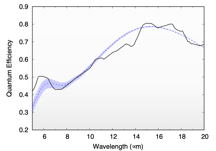
The agreement of our model with the measurements of the detector array with a single-layer anti-reflective coating optimized for 16 m demonstrates that the internal operation of the detectors is well understood for the 5 10 m range. We therefore confirm that even higher QEs are expected in this range with a suitably optimized antireflective coating. Ressler et al. (2008) show a predicted value of 60%.
3.2 Detector gain?
The agreement between model and measurements in Figure 4 emerges in a straightforward way, based on a careful accounting of all the relevant effects. In an alternative approach, Woods et al. (2011) invoked detector gain at the wavelengths short of 10 m, i.e. a quantum yield 1.222There are two common definitions of quantum yield (QY). In one, used by Woods et al. (2011), it describes the number of charge carriers produced per incident photon. In the other, which we prefer, there are two terms: (1) the QE is the fraction of incoming photons absorbed to produce free charge carriers, i.e., a peak of 0.78 or 78% in Figure 4, and (2) the QY is the average number of charge carriers produced per absorbed photon, i.e. 1.66 at 5.6m in the Woods et al. (2011) analysis. Under their definition, the QY would be the QE multiplied by the QY as we define it. In our definition, the detector noise can be as small as the square root of the product of the photon flux and the QE, and QY 1 leads to extra noise terms. We find that this is not necessary and is in fact unlikely. QY 1 is improbable in extrinsic photoconductors (for photons below their bandgap energies) because the impurities that need to be ionized are so dilute in the crystal. In addition, gain in these detectors would be associated with increased noise above the simple square root of the number of absorbed photons. Two effects are relevant: (1) the excess electrons over those for QY = 1 are not independent; the number of independent events is the number of absorbed photons, not the number of resulting photoelectrons; and (2) the statistical fluctuations in the number of photoelectrons produced per photon means that the noise will be increased further. As an example of the first effect, at 5.6 m, Woods et al. (2011) predict QY = 1.66; therefore the number of independent absorbed photons will have been overestimated by this factor. Assuming the signal to noise ratio (SNR) goes as the square root of the number of absorbed photons, the SNR will be overestimated by a factor of 1.29. We simulated the second effect with a Monte Carlo calculation. This calculation allowed each simulated photon to produce 1, 2, or 3 photoelectrons and calculated the resulting signals as a 1000 second integration sampled every 3 seconds (analogous to the operation in MIRI). The resulting integration ramp was fitted by linear regression and the results compared as a function of the QY. For QY = 1.66, the prediction from this simulation is that the noise should be increased a further factor of 1.14. That is, the value of the QY found by Woods et al. (2011) implies that the noise at 5.6 m should be elevated by a total factor of 1.29 1.14 = 1.47 over that estimated from the square root of the number of collected charge carriers.
This prediction has been compared with the measured noise from the MIRI detectors. We used calibration data obtained in the JWST Cryo-Vacuum Test 3 (CV3) to determine the noise. A series of measurements was taken in each imager filter (except 25.5 m), with the total collected electrons adjusted to be approximately the same in all cases. These data were reduced to a series of images. Adjacent images were differenced to remove non-ideal behavior (e.g., reset anomaly, drifts) and photometry was conducted on the resulting images using a pseudo-aperture approach in which the “source” region is square and the “sky” is a surrounding square with the center removed, with all dimensions an integral number of pixels. The “signal” is then the total counts from the “source” minus the predicted number of counts adjusted to the same number of pixels from the “sky”. This extraction unit was placed randomly (except it was always centered on a pixel) over the difference image to obtain a Monte Carlo set of noise measurements. This geometry allows very straightforward calculation of the expected noise since both source and sky contain an integral number of pixels. We found a modest degradation of the detector noise behavior toward short wavelengths, by a factor of 1.15 at 5.6 m. This effect could have a number of possible causes; for example, instability in the source temperature will modulate the output flux more at the short wavelengths than at the long ones. Assuming the entire effect is true photon-noise-related, it is significantly less than predicted for the QY reported by Woods et al. (2011), i.e., the factor of 1.47 based on the photon statistics and our Monte Carlo simulation combined.
In the preceding section, we reproduced the full wavelength-dependent behavior of the MIRI detector quantum efficiency with QY = 1. Given this experimental evidence against values significantly above 1, we believe QY = 1 is correct for these devices operating at wavelengths 5 m.
4 “Banding” or the “cross” artifact
A general issue for back-illuminated semiconductor photodetectors arises when the absorption efficiencies are low, allowing some photons to penetrate to the frontside from which they are scattered back into the detector array. Particularly if the array is thick, they can be absorbed and detected far from their point of entry. For example, for ACS on HST: “Long wavelength photons that pass through the CCD can also be scattered by the electrode structure on the [front] side of the device. This creates two spikes that extend roughly parallel to the x-axis. These spikes are seen at wavelengths longer than 9500 Å in both the HRC and WFC” (Ryon, 2019). Similarly for the STIS on HST: “Longward of 6000 Å, the scattered light component becomes noticeable, primarily due to scatter in the STIS CCD and climbs to a level of at 10,000 Å” (Gull et al., 2003).
A cross artifact due to this phenomenon at wavelengths 10 with Si:As IBC detectors was first noticed in the Channel 3 and 4 IRAC/Spitzer images (Pipher et al., 2004); see Figure 5. It can be described as a few rows and columns of bright pixels centered on a point source, with the artifact becoming brighter towards the source. The discussion below explores the causes of these internal scattering artifacts, focusing on Si:As IBC detectors, and demonstrates a theoretical simulation of them. That is, while Section 3 focused on the traditional type of response, trajectories (1) (4) in Figure 1, we now focus on trajectory (5) and its further reflections. Since the analysis is computationally demanding, we simplify it by ignoring reflection at the buried contact, which is only at a level. Enabling reflection would significantly increase computational complexity by allowing a large number of additional photon paths, which would need to be tracked. Ignoring reflection at the buried contact has no significant effect on the results because it is an insignificant player in the response being modeled. We have verified this with a modification of our modeling code.
4.1 Details of the Si:As IBC detector behavior
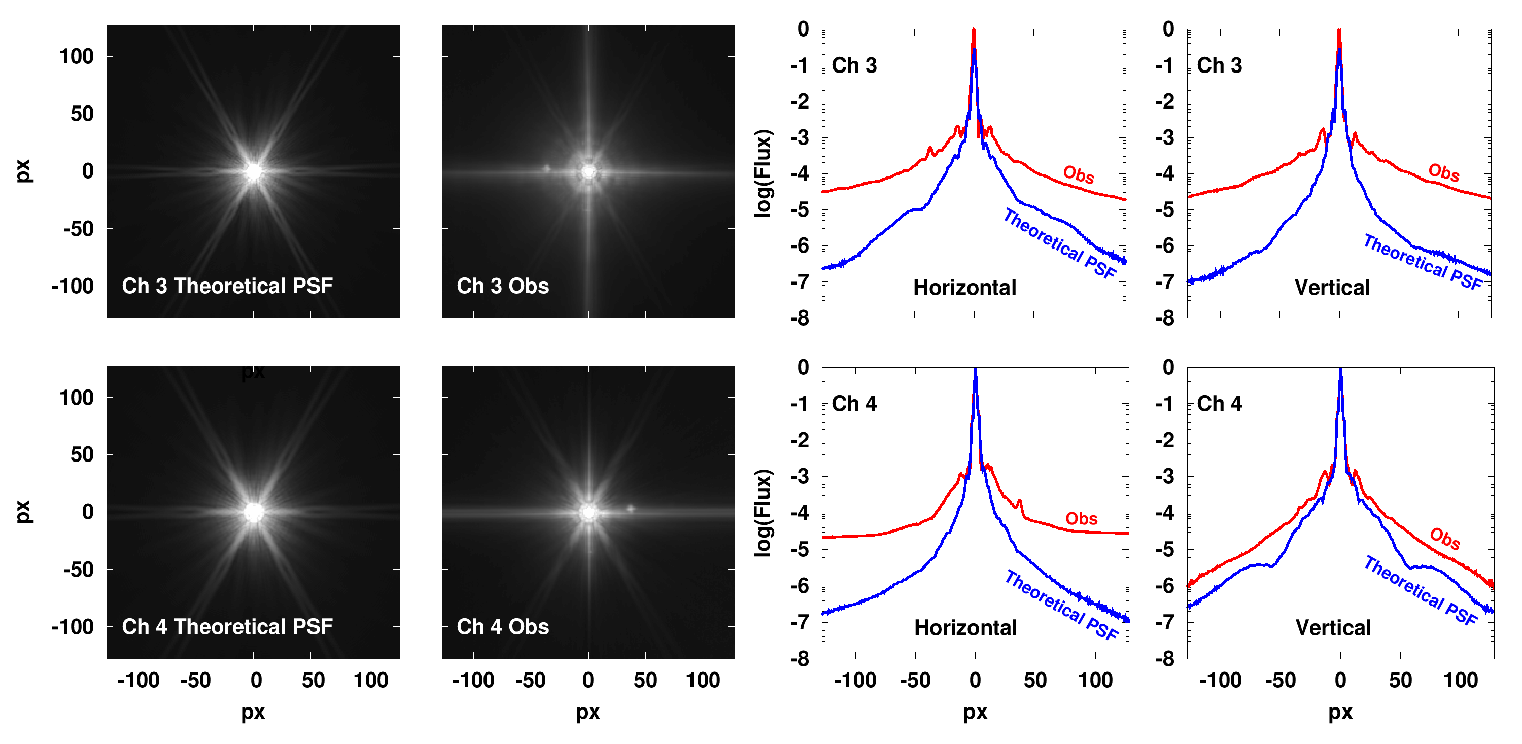
In Figure 5, we show theoretical and in-flight observed point spread functions (PSFs) for the IRAC instrument, highlighting the considerable difference between the two. The Spitzer Science Center (SSC) pipeline notes that the artifact exhibits flaring and that narrow-band images have a more complex artifact pattern. Since IRAC had a dedicated detector at each wavelength and the PSFs could be well characterized, there were no additional attempts to understand the nature of the artifact theoretically.
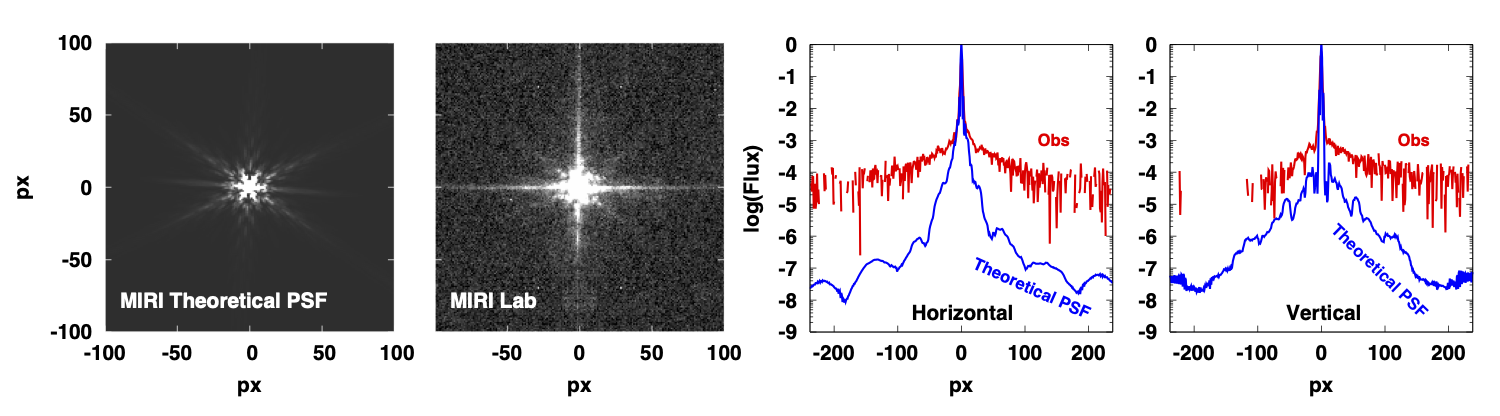
A similar “cross” also appears in the MIRI detector images. In Figure 6, we show the theoretical PSF calculated with WebbPSF v. 0.8.0 (Perrin et al., 2012, 2014) and images taken with the flight detector at the second cryo-vacuum test (with certain artifacts related to the laboratory setup artificially removed from the image), both at . Remarkably, the artifact is present out to at least pixels in the high contrast laboratory images. As we show below, the artifact is a result of two optical properties of the detectors: 1) coherent light beams undergo diffraction off the metallic pixel contacts at the frontside of the detectors, and 2) inefficient photon absorption at shorter wavelengths ( µm) in the IR-active layers and reflection off both the front and the back of the detector allows photons to travel through the detector multiple times. A pass through the detector and substrate three times (down, up, and down) produces an artifact extending to a maximum of px, meaning some of the photons cross the MIRI detector at least two times to be detected at a distance of over 400 px. At 400 px the WebbPSF contrast is , while the standard deviation of the background in the CV2 data is at a contrast of . The cross is 1 above the background up to 150 px from the central source and is visually discernible to 400 px.
4.2 The Quantum Electrodynamic model of the detector
Since we were uncertain of details regarding the scattering/diffraction, we could not a-priori determine a simple specific model. Furthermore, our input light sources are more complicated than just a pinhole and realistic PSFs change as a function of wavelength. Therefore, we model the detector using the theory of Quantum Electrodynamics (QED; Feynman, 1948); as an all-encompassing Monte Carlo-style (MC) method it allows us to model aspects of the system we otherwise may have ignored.
4.2.1 Basics of QED
With QED modeling, all possible random directions of ray paths need to be explored, even if they violate classical optical laws. Each ray path carries its own probability amplitude and phase angle (or complex phasor), where the phase angle advances with traveled distance as
| (1) |
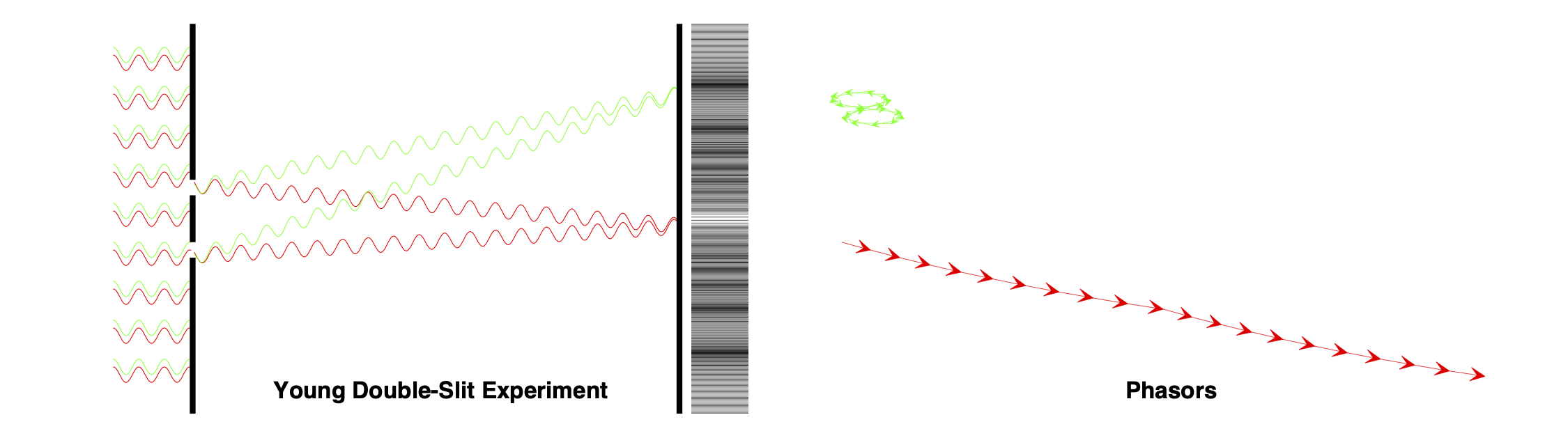
where is the wavelength of the tracer and is the traveled distance. As the photons enter the silicon substrate from the outer vacuum their wavelengths shorten by a factor of n, i.e. a 5.6 m photon will become a 1.64 m photon. We quote the vacuum equivalent wavelength of photons in our work; however, the calculations use the appropriately shortened wavelengths. The phasors of unlikely paths cancel out, while the phasors of likely paths construct a large probability amplitude due to their similar phase angles. The resulting map of the square of the amplitudes yields the final relative probability of a photon being absorbed at a certain location and hence the intensity. In Figure 7, we explain the Young double-slit experiment with QED modeling, showing how the probability amplitudes at various locations add up. The total amplitude at the intensity peak is much larger than at the minima.
4.2.2 Tracer paths
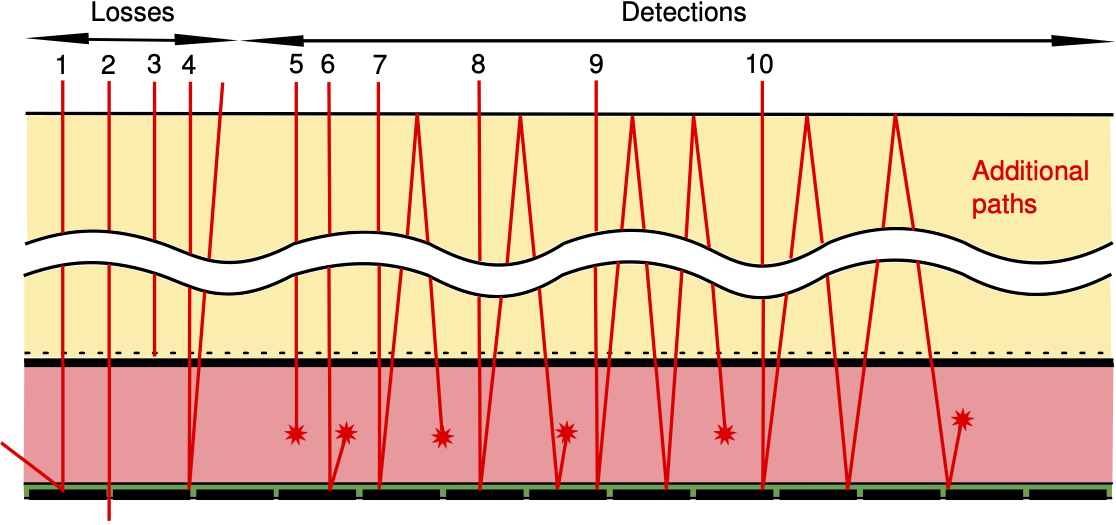
We first describe how photons creating the cross artifact travel in the detector and then how the QED model describes the probability of each path. In Figure 1, we showed two possible paths with minor variations. In Figure 8, we show how diffracted photons ((5) in Figure 1) can be returned to the active pixels by total internal reflection off the array backside. We expand on this figure and show the most likely 10 paths a photon may take in Figure 9, with the probabilities of each path noted in Table 1. Paths 1 6 are variations of those from Figure 1, but paths 7 10 illustrate the cases for photons trapped by total internal reflection and show how they may travel many pixel widths within the detector array before being absorbed, detected, or lost. This process is relatively efficient because of the good transparency of the buried contact at short wavelengths as shown in Figure 3. Although theoretically there are an infinite number of possible paths for the photons to take through the detector, 99% of the photons will travel on the most probable dozen or so path-types (see Table 1).
| Path ID | Description | Percent |
|---|---|---|
| Losses | ||
| 1 | Exit at the side of the detector | 0.11% |
| 2 | Exit in the pixel gap | 9.39% |
| 3 | Absorption at the buried contact | 1.03% |
| 4 | Exit at the top of the detector | 1.79% |
| Detections | ||
| 5 | Absorption in 1st pass | 27.09% |
| 6 | Absorption in 2nd pass | 35.63% |
| 7 | Absorption in 3rd pass | 11.91% |
| 8 | Absorption in 4th pass | 7.68% |
| 9 | Absorption in 5th pass | 2.56% |
| 10 | Absorption in 6th pass | 1.65% |
Note. — The sum of all losses and the eleven most probable detected tracer paths encompass 99.98% of all possible paths. Tracer path IDs larger than 10 are not shown in Figure 9; they are simply further crosses across the detector. Surprisingly, of the photons/tracers are lost through various modes. The first two detection paths will remain close to the image core and contain 63% of the total flux (the detection within the second passing - path #6 - is higher than in the first, due to increased pathlengths from off-axis diffraction). Around 26% of the total flux will be spread out (i.e. not absorbed in the first two crossings of the IR active layer), remaining in the detector and raising the “background” signal or contributing to the cross artifact. Our model ignores an reflection at the buried contact.
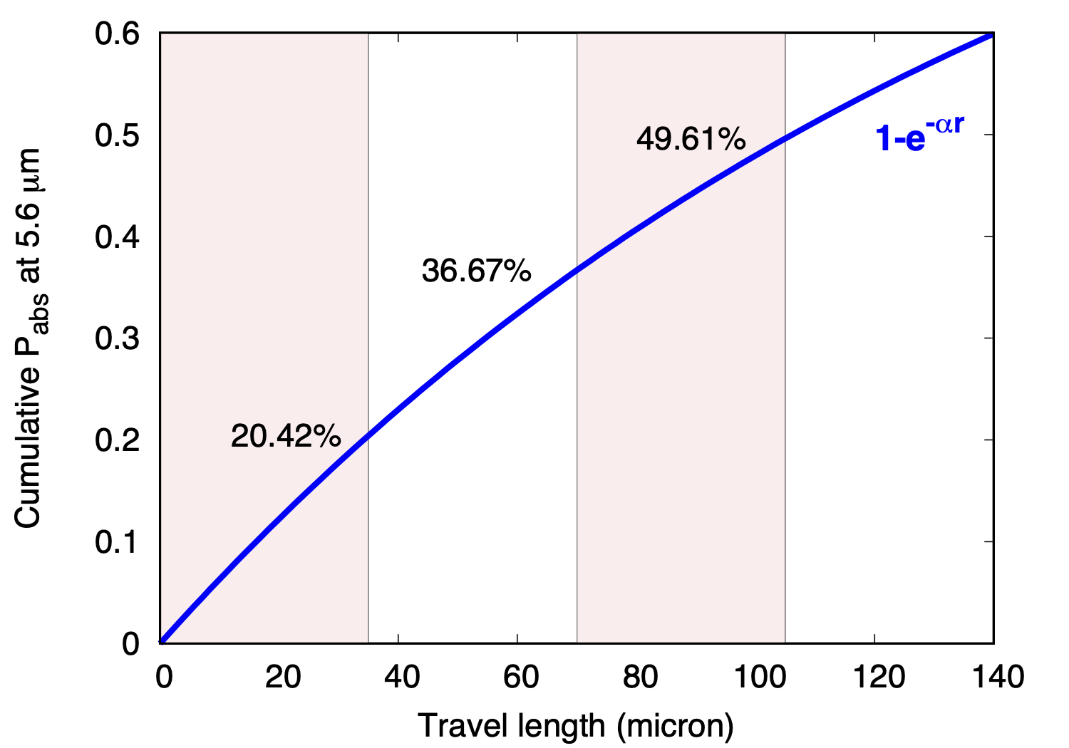
When describing the QED model, we use the word “tracer” to describe a particular photon path that is explored. We do this to differentiate it from paths that photons are more likely to take. Each tracer enters the detector with the same initial phase angle and unit amplitude. The total path length covered by the tracers is cumulatively monitored and used to calculate the phase angle when and if they are absorbed. As a tracer travels trough the buried contact, it may either get absorbed (and vanish from the calculation) or transfer through it, according to the absorptance illustrated in Figure 3. As noted previously, we ignore reflection at the buried contact, due to its low probability and the computational simplifications this allows. The tracer then travels through the IR-active layer and either gets absorbed or survives its passage. The probability of absorption is described as
| (2) |
where is the distance traveled in the IR-active layer and is the absorption efficiency, which we derive from the fitted QE, i.e. the values as shown in Figure 2 adjusted to optimize the fit as in Figure 4. In Figure 10, we show how the probability of absorption increases for 5.6 m wavelength photons with the cumulative distance traveled in the IR-active layer.
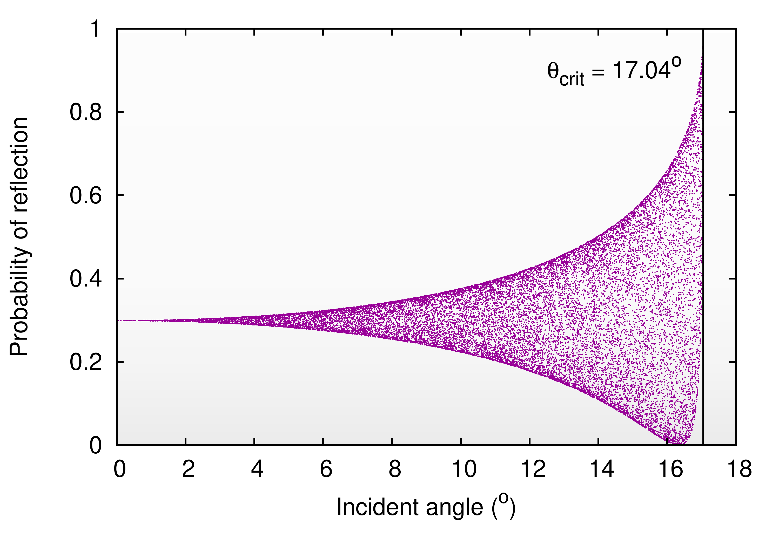
The total length that is travelled through the IR-active layer will depend on the incidence angle of the tracer, which is practically 0∘ for the first passage (ignoring minor variations due to OTA diffraction). If a tracer survives, it will get reflected off the metallic contacts at a random angle or disappear in the pixel gaps between the metallic contacts. Since in this section we are modeling the diffraction pattern, and the only surface yielding one is the pixel lattice, we generate new random directions for the tracers only at the metallic contacts and evolve them following regular reflection laws at the reflecting surface (hence the unusual reflection angle for the paths in Figures 1 and 9). This allows us to calculate the model with a “reasonable” number of photons. A reflected/diffracted tracer will assume its new direction and continue to travel toward the detector backside, with similar physical considerations as on the way from the backside to the frontside. For incidence angles larger than 0∘, the travelled length will increase and therefore so will the absorption probability (see Figure 10) in the IR-active layer. The final fork in the road traveled by a tracer is at the backside, where it will either exit the detector or be reflected and repeat the previous cycle. Whether a tracer reflects or not depends on its incidence and polarization phase angles, and the probability is given by the Fresnel equations. If the incidence angle is larger than the critical angle of total internal reflection
| (3) |
then the tracer reflects with a nearly 100% probability (since the AR coating is virtually lossless). If this incidence angle is less, then we need to apply the Fresnel equations. Since most astronomical objects are not polarized, the model picks a random polarization angle and calculates a reflection probability. In Figure 11, we show the reflection probabilities of 50,000 tracers in the code, highlighting the large range of probabilities considered for the majority of incidence angles.
Since the patterns will likely form on spatial scales proportional to the input wavelength (which is reduced by a factor of nsil once the photon enters the silicon detector), we divide each pixel into sub-pixels and calculate the phasor amplitudes as if the photons were absorbed in the center of the sub-pixels. The default setting of the model is to use 1 µm sub-pixels, which is close to Nyquist sampling the 1.64 µm wavelength of a 5.6 µm input photon after it enters the silicon. The model can also divide the IR-active layer into sub-layers, although this division has little effect. Absorption is calculated in the center of the sub-layers; if a single absorptive layer is assumed (as in the default setting), then absorption is projected to occur in the middle of the IR-active layer.
4.2.3 Image flux scaling
We sample tracers from the square root of the initial intensity distribution and track the position and phase of their phasors as they travel in random directions. Sampling from the square root of the intensity distribution is necessary, as photon probabilities (i.e. intensities) are defined as the square of the total phasor amplitude. Therefore, to select unit amplitude tracers with correct probabilities, we need to sample them from the square root of the input intensity distribution. If a tracer is absorbed, we add its phasor to the total phasor in the respective sub-pixel it was absorbed in. When choosing from an input image or Airy ring, spatial positions are determined randomly based on cumulative flux distributions, thereby selecting brighter input positions more frequently than fainter ones.
We also need to track the number of tracers absorbed and initiated, as it is necessary to scale the relative probabilities. The vast majority of tracer paths are low probability, but their low probability needs to be established with a large number of test paths. Therefore, the model records each probable photon path type separately, being able to distinguish between the most probable photon paths. This is important because the final relative intensity map is calculated as the square of the phasor amplitudes, scaled by the total number of photons absorbed relative to the number of photons the model used. In equation form, the total intensity of a particular path at pixel position would be described by
| (4) |
where gives the total number of tracers absorbed in path , gives the total number of test tracers used by the program, the amplitude squared in pixel (x,y) for path , while is the total intensity captured with path .
As many more photons are absorbed in the first photon passing, and probabilities are calculated as relative differences between sums, it would receive a significantly higher flux value if we did not correct for the number of photons each path (and layer) possibility (each with its own diffraction pattern) absorbed. This is an important aspect of QED; it calculates relative probabilities using sums. Furthermore, each absorption event is independent; there is no “interference” in QED in the classical sense (even though the final product is equivalent). Once a large enough number of tracers has been recorded for each possible path and absorption layer, we calculate intensity maps for each path-type and sum them up per pixel. Finally, the intensities of all path-types are summed for the total intensity per pixel.
4.2.4 Our modeling code GimMIRI
Unfortunately, MC algorithms are notoriously slow to converge, therefore our modeling code utilizes graphical processing units (GPUs). GPUs, with their parallel processing capabilities, provide an ideal environment for calculating the trajectories of independent tracers; hence they are widely used in ray tracing applications. We opted to encode our model using the Nvidia CUDA language, since the University of Arizona has a substantial Nvidia GPU cluster server333https://elgato.arizona.edu/ and we have also received an academic hardware donation directly from Nvidia. The code we developed, called GimMIRI (GPU image for MIRI), is a multi-GPU single-node program written in C/CUDA, allowing it to use as many GPUs as are available (or requested) on a single computer node. 444Download from https://github.com/merope82/GimMIRI The model only has a few basic input variables and a multitude of tweakable detector parameters that are defined and hard-coded in the source. The calculations are done at a single wavelength (which is one of the input variables) for each execution of the code and therefore if an extended bandpass is studied, multiple models need to be run and their results co-added. The user can select between three flux input distribution types: 1) any fits file of their liking, 2) a pinhole of chosen radius, or 3) an Airy function (specified by the observing aperture). If a WebbPSF (Perrin et al., 2014) PSF fits file is used as input, the code sets the wavelength and oversampling rate for the calculation from the image header (which can be overwritten). Other than output frequency and naming options, the only variable the user sets for the compiled code is x and y pixel offsets.
Each individual CUDA thread calculates the path of a single tracer, generating numerous independent random numbers during the calculations: assigning new random angles of propagation at the metallic contacts, deciding whether a tracer is absorbed in the IR-active layer or the buried contact, and setting reflection probabilities based on random polarization angles at the backside of the detector. To ensure that each thread generates independent random numbers, all threads on all cards have their unique random generator seed that is stored on the graphical cards. Up until absorption, all threads calculate independently, and upon absorption an atomic addition process (serialized) adds the tracer phasor values to the specific sub-pixel’s cumulative value. Since it is not likely that two threads will add to the same exact subpixel, the atomic addition does not slow down the code. At requested intervals the code writes a new fits image, with the image header containing all relevant information.
4.2.5 Variables of the model
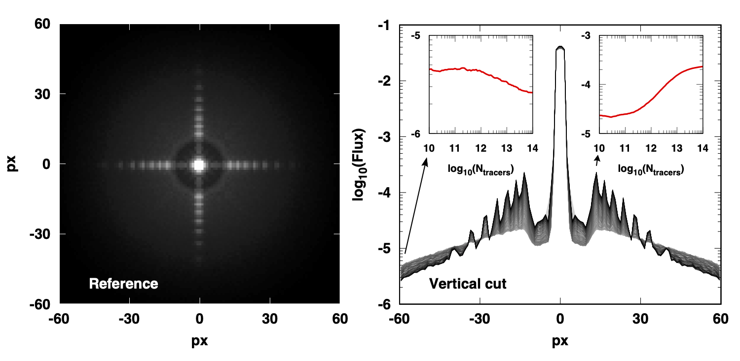
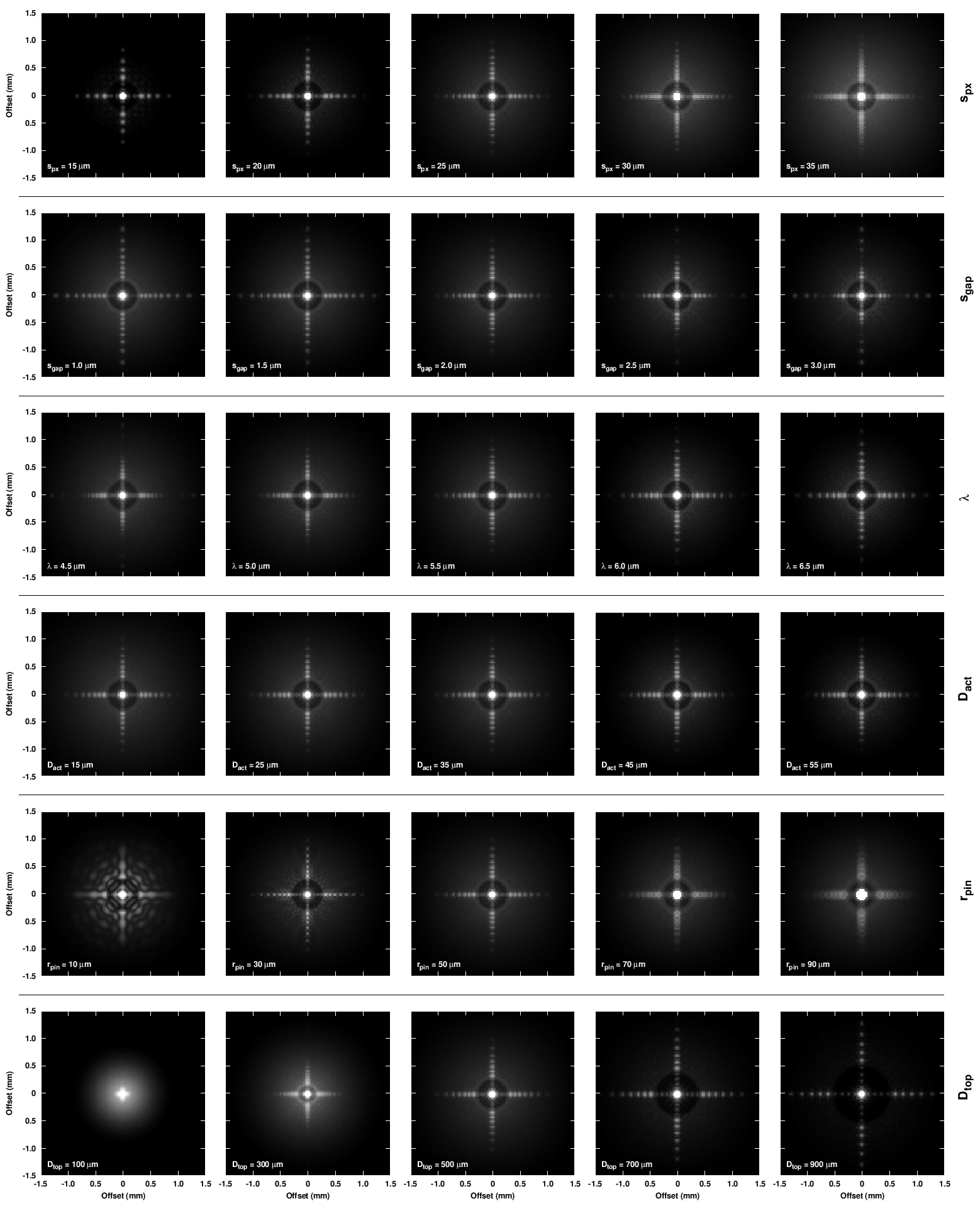
The variables of the model define the detector architecture, the finesse of the calculation, and the size of the output image. In Table 2, we define these variables and their values used in our reference model. Since the exact values of some of these variables are not available, we use reasonable assumptions for the MIRI detector. We execute a Reference model at 5.5 , assuming a 50 radius pinhole as input flux distribution. While the pinhole is obviously not representative of an actual PSF, its simplicity and concentrated light allows our model to converge faster and enables a clearer study of each detector parameter. In Figure 12, we show our Reference model image.
4.3 Exploring the parameter space
| Variable | Description | Value |
|---|---|---|
| Width of IR-active layer | 35.0 µm | |
| Total height of detector | 500.0 µm | |
| Pixel gap size | 2.0 µm | |
| Pixel pitch | 25.0 µm | |
| Sub-pixel size | 1.0 µm | |
| Input wavelength | 5.5 µm | |
| Pinhole radius | 50 µm | |
| Number of paths considered | 9 | |
| Number or IR sub-layers | 1 | |
| Refractive index of material | 3.4127 | |
| Output image size in x | 120 | |
| Output image size in y | 120 | |
| Offset in incident angle (normal) | 0.045∘ | |
| Offset in incident angle (CCW) | -13.75∘ |
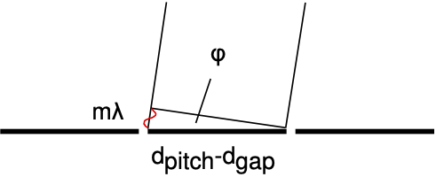
The diffraction pattern that is imaged depends on the various geometric parameters of the detector and the observed wavelength. As a first order approximation, the classic wave interference explanation of diffraction can help place each of them in context. In Figure 13, we display the direction of two beams at the top of a pixel-defining metallic contact, where the two beams constructively interfere at the order. Based on this interpretation, one would expect constructive interference, where
| (5) |
In the far field extreme, the two beams meet at infinity and the pixel offset can be calculated as
| (6) |
Since the height of the detector () is only 20 times that of the lattice length (and around 300 times the wavelength), the far field approximation is not necessarily adequate for modeling, but we can use it for demonstration purposes. For the reference model, the pixel offsets of the through 10 order peaks are at 2.8, 5.7, 8.6, 11.7, 15.0, 18.5, 22.5, 27.1, 32.5, and 39.3 pixels, according to the far field approximation. In fact, we see peaks in the diffraction pattern for the reference model at , 16.5, 19.6, 23.5, 27.9, 33.0, and 39.6 pixel offsets, corresponding to the to 10 orders. The , 2, 3 orders fall inside the critical angle of total internal reflection and are therefore not produced at a high contrast level. The agreement between the far field approximation and model results is worse for the lower orders, as the pathlength of the rays is shorter for them. For , the difference is less than a pixel for the reference model. Obviously, the level of agreement will depend on the detector architecture and the wavelength of observation. At , the diffraction angle would be larger than 90∘ and therefore it is not physically plausible; the diffraction angle is 78.8∘ and the pixel offset is px. This calculation also shows that any artifact that extends over this distance must be produced by more than a single reflection off the metallic contacts.
We modeled the diffraction pattern as a function of varying values for the pixel pitch (), the pixel gap (), the input wavelength (), the detector substrate height (), the size of the pinhole radius (), and the width of the IR-active layer (). In Figure 14, we show the GimMIRI image as a function of these variables. The details of the pattern change, but the overall pattern remains and is dominated by the diffraction off the square grid of contacts. Other dominant patterns would result from other contact geometries.
We conducted a number of tests to be sure of the validity of our models. We checked for numerical convergence in Figure 12. The GimMIRI reference model is converged by 1014 tracer phasors. When modeling realistic PSFs, more tracers are necessary, therefore we will check for convergence again when modeling the JWST PSF responses at higher fidelity. We also checked dependence on the sub-pixeling and the number of sub IR-active layers we model. Nyquist sampling with sub-pixeling is critical, however, sub-layering the IR-active layer is not as important, as long as absorbed photons are projected to be absorbed in the center of the layer.
5 Verifying our QED model
We verify our QED diffraction model against the artifact pattern observed in the MIRI CV2 tests. For this test, we used the WebbPSF model of MIRI at 5.6 m as the input flux distribution. It models the complete JWST optical path up to the instrument focal plane, and therefore provides the ideal input flux distribution for our model. To simulate a realistic smooth input PSF, we used a 16 times ovsersampled WebbPSF model for our calculations. Calculating the GimMIRI image (to tracers) took a total of 1200 hours on two Nvidia TITAN BLACK GPUs.
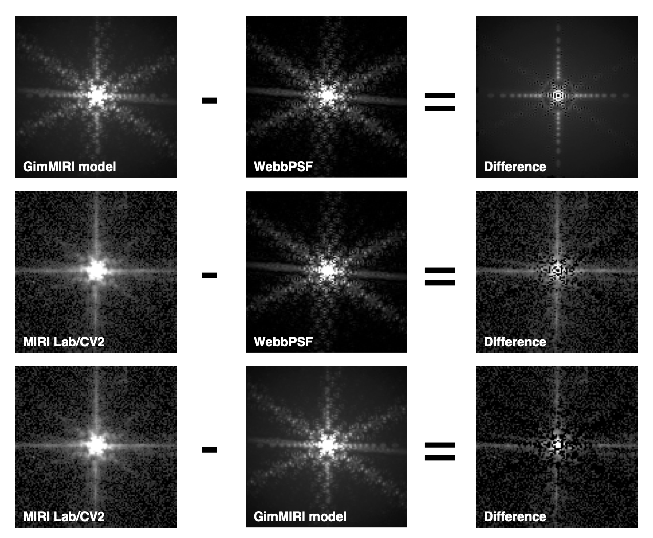
The WebbPSF model has an integrated unit intensity (by definition), while the modeled GimMIRI PSF has an integrated intensity of 0.835. This shows that 83.5% of the incoming flux remains within the detector; the increase compared with the QE calculated for the central response only in Section 3 is an indication of the extent of the diffraction effects. The number is also slightly lower than the cumulative absorbed value given in Table 1, as the verification model “only” encompassed a 200 px 200 px area, resulting in higher losses at the detector edge. The peak intensity of the PSFs, however, scale by a factor of 0.624, which agrees with the QE values estimated by Ressler et al. (2008) and in Section 3 for a device with an AR coating optimized for 6 m. The difference between the two scalings highlight that a significant portion (21.2%) of the flux gets placed into both the diffraction spikes and into a halo surrounding the peaks, and also the problems posed by the artifacts when calibrating spectral data.
In Figure 15, we compare the theoretical JWST/MIRI PSF calculated with WebbPSF to the complete PSF calculated with GimMIRI, and with that measured using a flight hardware at the second cryo-vacuum tests (CV2). All images are at 5.6 µm (at native pixel scale). The cross artifact is apparent in both the observed PSF and the modeled one, although modeling with additional photon tracers would likely strengthen its signal in the final model image. The top row of Figure 15 shows the output GimMIRI PSF image and the WebbPSF model that was used as the input for the modeling, as well as their difference. The top-right panel highlights where the internal diffraction places the flux removed from the PSF core. The middle-row of Figure 15 shows the difference between the measured CV2 PSF and the WebbPSF model. It is clear that the WebbPSF is not adequate to model the observed diffraction structure. The bottom row of Figure 15 compares the CV2 image with the GimMIRI one. Our model removes the PSF core and most of the diffraction pattern, but not the complete structure. This is due at least in part to the fact that the laboratory image was taken using the F560W MIRI filter, which has a broad transmission window within 5.0 and 6.2 µm, while the GimMIRI model is at a single wavelength. The broader transmission profile will result in a smooth diffraction spike, which the single wavelength model cannot replicate.
Our model reproduces the cross artifact produced by tracers up to path #8 in Figure 9, which can physically extend up to 200 px. The artifact can be traced further out at very low levels (see Section 4.1) in actual images. While our model does include these unlikely tracer paths, modeling constructive interference with QED tracers at those distances is very expensive computationally. Further work will be necessary to enable quicker (and possibly less accurate) modeling of the diffraction structure. Regardless, GimMIRI provides a complete model of all the attributes of the detector physics, thereby providing a baseline for future approximations.
6 Summary
We have addressed two phenomena regarding the short wavelength (5 10 m) performance of Si:As IBC detector arrays: (1) quantum efficiency; and (2) image artifacts. Our study confirms:
-
•
Quantum efficiencies in the 5 10 m range of 60% are attainable with these detectors when suitably anti-reflection coated.
-
•
This performance is achieved without quantum yields (QYs; i.e. the number of free charge carriers yielded per absorbed photon) 1. There should be no excess noise as would result if QY 1.
At wavelengths of 5 10 m, these detectors show a large-scale cross-like imaging artifact. Related behavior is seen in other back-illuminated solid-state detectors where the absorption efficiency is low, e.g. conventional CCDs in the near infrared, allowing photons to scatter off contacts and other structures on the detector frontside. We show that
-
•
The underlying cause of these artifacts is low absorption efficiency at the particular wavelength and diffraction off inter-contact gaps
-
•
Photons can be diffracted to sufficiently large off-axis angles ( in silicon) that they are totally reflected when they reach the detector backside.
-
•
Consequently, these photons can be trapped in the detector/substrate wafer and can travel large distances until they are absorbed or escape, often leading to their detection far from their point of entry.
References
- Argyriou et al. (2020) Argyriou, I., Wells, M., Glasse, A., et al. 2020, A&A, 641, A150, doi: 10.1051/0004-6361/202037535
- Coon & Karunasiri (1986) Coon, D. D., & Karunasiri, R. P. G. 1986, Phys. Rev. B, 33, 8228, doi: 10.1103/PhysRevB.33.8228
- Estrada et al. (1998) Estrada, A. D., Domingo, G., Garnett, J. D., et al. 1998, in Proc. SPIE, Vol. 3354, Infrared Astronomical Instrumentation, ed. A. M. Fowler, 99–108
- Fazio et al. (2004) Fazio, G. G., Hora, J. L., Allen, L. E., et al. 2004, ApJS, 154, 10, doi: 10.1086/422843
- Feynman (1948) Feynman, R. P. 1948, Rev. Mod. Phys., 20, 367, doi: 10.1103/RevModPhys.20.367
- Geist (1989) Geist, J. C. 1989, Appl. Opt., 28, 1193, doi: 10.1364/AO.28.001193
- Gull et al. (2003) Gull, T. R., Lindler, D., Tennant, D., et al. 2003, in HST Calibration Workshop : Hubble after the Installation of the ACS and the NICMOS Cooling System, 147
- Hawkins & Hunneman (2004) Hawkins, G., & Hunneman, R. 2004, Infrared Physics and Technology, 45, 69, doi: 10.1016/S1350-4495(03)00180-4
- Hoelzlein et al. (1980) Hoelzlein, K., Pensl, G., & Schulz, M. 1980, Applied Physics, 23, 7, doi: 10.1007/BF00899563
- Hora et al. (2004) Hora, J. L., Fazio, G. G., Allen, L. E., et al. 2004, in Proc. SPIE, Vol. 5487, Optical, Infrared, and Millimeter Space Telescopes, ed. J. C. Mather, 77–92
- Ilaiwi & Tomak (1990) Ilaiwi, K., & Tomak, M. 1990, Journal of Physics and Chemistry of Solids, 51, 361, doi: 10.1016/0022-3697(90)90120-5
- Laine (2015) Laine, S., ed. 2015, IRAC Instrument Handbook
- Leech et al. (2003) Leech, K., Kester, D., Shipman, R., et al. 2003, The ISO Handbook, Volume V - SWS - The Short Wavelength Spectrometer
- Li (1980) Li, H. H. 1980, Journal of Physical and Chemical Reference Data, 9, 561, doi: 10.1063/1.555624
- Lisowski & Skopec (2009) Lisowski, M., & Skopec, A. 2009, IEEE Transactions on Dielectrics and Electrical Insulation, 16, 24, doi: 10.1109/TDEI.2009.4784548
- Love et al. (2006) Love, P. J., Beuville, E. J., Corrales, E., et al. 2006, in Society of Photo-Optical Instrumentation Engineers (SPIE) Conference Series, Vol. 6276, Proc. SPIE, 62761Y
- Love et al. (2004) Love, P. J., Hoffman, A. W., Lum, N. A., et al. 2004, in Society of Photo-Optical Instrumentation Engineers (SPIE) Conference Series, Vol. 5499, Proc. SPIE, ed. J. D. Garnett & J. W. Beletic, 86–96
- Love et al. (2005) Love, P. J., Hoffman, A. W., Lum, N. A., et al. 2005, in Proc. SPIE, Vol. 5902, Focal Plane Arrays for Space Telescopes II, ed. T. J. Grycewicz & C. J. Marshall, 58–66
- Mainzer et al. (2008) Mainzer, A., Larsen, M., Stapelbroek, M. G., et al. 2008, in Proc. SPIE, Vol. 7021, High Energy, Optical, and Infrared Detectors for Astronomy III, 70210X
- Mill et al. (1994) Mill, J. D., O’Neil, R. R., Price, S., et al. 1994, Journal of Spacecraft and Rockets, 31, 900, doi: 10.2514/3.55673
- Onaka et al. (2007) Onaka, T., Matsuhara, H., Wada, T., et al. 2007, PASJ, 59, S401, doi: 10.1093/pasj/59.sp2.S401
- Perrin et al. (2014) Perrin, M. D., Sivaramakrishnan, A., Lajoie, C.-P., et al. 2014, in Proc. SPIE, Vol. 9143, Space Telescopes and Instrumentation 2014: Optical, Infrared, and Millimeter Wave, 91433X
- Perrin et al. (2012) Perrin, M. D., Soummer, R., Elliott, E. M., Lallo, M. D., & Sivaramakrishnan, A. 2012, in Proc. SPIE, Vol. 8442, Space Telescopes and Instrumentation 2012: Optical, Infrared, and Millimeter Wave, 84423D
- Petroff & Stapelbroek (1980) Petroff, M. D., & Stapelbroek, M. G. 1980, ”Blocked impurity band detectors”, Google Patents
- Petroff & Stapelbroek (1984) —. 1984, Proceedings of the Meeting of the Specialty Group on Infrared Detectors, IRIA-IRIS, 2
- Petroff & Stapelbroek (1985) —. 1985, Proceedings of the Meeting of the Specialty Group on Infrared Detectors, IRIA-IRIS, 3
- Pipher et al. (2004) Pipher, J. L., McMurtry, C. W., Forrest, W. J., et al. 2004, in Proc. SPIE, Vol. 5487, Optical, Infrared, and Millimeter Space Telescopes, ed. J. C. Mather, 234–243
- Ressler et al. (2008) Ressler, M. E., Cho, H., Lee, R. A. M., et al. 2008, in Society of Photo-Optical Instrumentation Engineers (SPIE) Conference Series, Vol. 7021, Proc. SPIE, 70210O
- Ressler et al. (2015) Ressler, M. E., Sukhatme, K. G., Franklin, B. R., et al. 2015, PASP, 127, 675, doi: 10.1086/682258
- Rieke et al. (2015) Rieke, G. H., Ressler, M. E., Morrison, J. E., et al. 2015, PASP, 127, 665, doi: 10.1086/682257
- Ryon (2019) Ryon, J. E. 2019, Advanced Camera for Surveys Instrument Handbook for Cycle 27 v. 18.0
- Stetson et al. (1986) Stetson, S. B., Reynolds, D. B., Stapelbroek, M. G., & Stermer, R. L. 1986, in Proc. SPIE, Vol. 686, Infrared detectors, sensors, and focal plane arrays, 48–65
- Szmulowicz et al. (1988) Szmulowicz, F., Diller, J., & Madarasz, F. L. 1988, Journal of Applied Physics, 63, 5583, doi: 10.1063/1.340335
- Szmulowicz & Madarsz (1987) Szmulowicz, F., & Madarsz, F. L. 1987, Journal of Applied Physics, 62, 2533, doi: 10.1063/1.339466
- Van Cleve et al. (1995) Van Cleve, J. E., Herter, T. L., Butturini, R., et al. 1995, in Society of Photo-Optical Instrumentation Engineers (SPIE) Conference Series, Vol. 2553, Proc. SPIE, ed. M. S. Scholl & B. F. Andresen, 502–513
- Woods et al. (2011) Woods, S. I., Kaplan, S. G., Jung, T. M., & Carter, A. C. 2011, Appl. Opt., 50, 4824, doi: 10.1364/AO.50.004824