Ultrafast Momentum-Resolved Probing of Plasmon Thermal Dynamics with Free Electrons
Abstract
Current advances in ultrafast electron microscopy make it possible to combine optical pumping of a nanostructure and electron beam probing with subångstrom and femtosecond spatiotemporal resolution. We present a theory predicting that this technique can reveal a rich out-of-equilibrium dynamics of plasmon excitations in graphene and graphite samples. In a disruptive departure from the traditional probing of nanoscale excitations based on the identification of spectral features in the transmitted electrons, we show that measurement of angle-resolved, energy-integrated inelastic electron scattering can trace the temporal evolution of plasmons in these structures and provide momentum-resolved mode identification, thus avoiding the need for highly-monochromatic electron beams and the use of electron spectrometers. This previously unexplored approach to study the ultrafast dynamics of optical excitations can be of interest to understand and manipulate polaritons in 2D semiconductors and other materials exhibiting a strong thermo-optical response.
I Introduction
Thermal engineering of plasmons and other forms of polaritons in nanomaterials offers an appealing way of controlling light-matter interactions down to nanometer Baffou and Quidant (2012) and femtosecond Ni et al. (2016); Dias et al. (2020) spatiotemporal scales, opening applications in photonics and optoelectronics, such as all-optical switching Debnath et al. (2018); Cox and García de Abajo (2019), light modulation Li et al. (2014); AbdollahRamezani et al. (2015); Yu et al. (2018), ultrafast light emission Kim et al. (2018), and photodetection Guo et al. (2018). Traditionally, the study of ultrafast thermal dynamics relies on optical experiments, in which a light pump pulse is used to excite the system and bring it out of equilibrium, followed by a light probe pulse that measures the evolution of the sample response Lui and Hegmann (2001); George et al. (2008); Wall et al. (2012). However, this procedure is limited in spatial resolution due to light diffraction when relying on far-field optics, or to a few tens of nanometers when a tip is used to locally amplify the electromagnetic field in ultrafast scanning near-field optical microscopy (SNOM) Ni et al. (2016).
Electron energy-loss spectroscopy (EELS) performed in scanning transmission electron microscopes overcomes the optical diffraction limit by using keV electrons rather than light to map the material response García de Abajo (2010); Kociak and Stéphan (2014); Polman et al. (2019) with subångstrom spatial precision Batson et al. (2002) and increasing spectral resolution that currently enables the study of mid-infrared polaritons Krivanek et al. (2014); Lagos et al. (2017); Hage et al. (2018, 2019); Hachtel et al. (2019). When the electron beam is well collimated, momentum-resolved inelastic electron scattering grants us access into the dispersion relations of surface modes in planar films Boersch et al. (1966a); Pettit et al. (1975); Chen and Silcox (1975a, b), while the dispersion of thicker samples can be probed with lower spatial resolution through low-energy (eV) electron microscopy in reflection mode Rocca (1995); Nagao et al. (2001). Additionally, a combination of high temporal and spatial resolution has been achieved through the development of ultrafast electron microscopy, based on the use of femtosecond light and electron pulses that are simultaneously aimed at the sample with a well-controlled relative delay Grinolds et al. (2006); Barwick et al. (2008, 2009). By scanning the light frequency, this approach additionally brings meV energy resolution in what is known as electron energy-gain spectroscopy (EEGS) Howie (1999); García de Abajo and Kociak (2008); Howie (2009), which has been experimentally demonstrated Pomarico et al. (2018) to challenge the state-of-the-art benchmark of a few meV achieved through tour-de-force advances in electron optics Krivanek et al. (2014). In the photon-induced near-field electron microscopy (PINEM) technique Barwick et al. (2009); García de Abajo et al. (2010); Park et al. (2010); Piazza et al. (2015); Feist et al. (2015); Lummen et al. (2016); Echternkamp et al. (2016); Priebe et al. (2017); Vanacore et al. (2018, 2019); Kfir et al. (2020); Wang et al. (2020), the electron beam is focused with nanoscale spatial precision, while the relative light-electron delay provides femtosecond temporal resolution. PINEM has been used to shoot femtosecond movies from surface plasmons evolving in nanowires Piazza et al. (2015) and buried interfaces Lummen et al. (2016), and more recently, also in the characterization of optical dielectric cavities Kfir et al. (2020); Wang et al. (2020). Although efforts in this context have emphasized light-matter interaction aspects and our ability to modulate the wave function of free-space electrons, the optical-pump/electron-probe (OPEP) approach has strong potential to study nanoscale dynamics with unrivalled spatiotemporal resolution by addressing material properties that range from relatively slow structural Grinolds et al. (2006); Barwick et al. (2008) and electronic Vogelgesang et al. (2018) behavior to the intrinsically ultrafast nonlinear optical response Konečná et al. (2019).
Two-dimensional (2D) materials offer a splendid testbed for OPEP because they generally undergo substantial changes in their electronic structure under optical pumping. We consider in particular highly-doped graphene, which in addition hosts electrically-tunable plasmons Jablan et al. (2009); Fei et al. (2011); Koppens et al. (2011); Chen et al. (2012); Fei et al. (2012); Yan et al. (2012a, b); Brar et al. (2013) that possess long lifetime Woessner et al. (2015); Ni et al. (2018), strong spatial confinement Lundeberg et al. (2017a); Alcaraz Iranzo et al. (2018), and a large nonlinear response Kumar et al. (2013); Yao et al. (2018); Kundys et al. (2018); Cox and García de Abajo (2019). These properties have prompted the exploration of exciting applications that include infrared photodetection Xia et al. (2009); Koppens et al. (2014); Lundeberg et al. (2017b); Guo et al. (2018); Yuan et al. (2020), optical sensing Rodrigo et al. (2015); Hu et al. (2016, 2019), and light modulation García de Abajo (2014); Gao et al. (2015); Yao et al. (2018); Cox and García de Abajo (2019); Dias et al. (2020). Because of its conical electronic band structure, the thermo-optical response is remarkably high in graphene and manifests in the emergence of plasmons in heated undoped samples Vafek (2006); García de Abajo (2014); Ni et al. (2016), as well as plasmon shifts when the electronic temperature is increased Jadidi et al. (2016); Yu et al. (2018). The effects are dramatic at electronic temperatures of a few 1000s K, which can be reached using femtosecond laser pulses without damaging the material Johannsen et al. (2013); Gierz et al. (2013). In this context, while SNOM has been extensively used to characterize graphene plasmons Fei et al. (2011); Chen et al. (2012); Fei et al. (2012); Ni et al. (2016, 2018), the unique combination of space, time, momentum, and energy resolution offered by OPEP makes it an ideal technique to reveal unexplored properties of those excitations, as well as other types of polaritons and their associated electron/lattice dynamics in 2D materials.
Here, we use predictive theory to demonstrate that the ultrafast OPEP approach can be used to characterize the temporal dynamics of plasmons in both extended and nanostructured graphene and graphite films. Specifically, we show that the strong confinement of plasmons in these materials produces large deflection in the inelastically scattered electrons, directly yielding dispersion curves in the energy-momentum-resolved electron transmission maps. Adjustment of the light/electron delay allows us to explore the temporal evolution of these excitations as the material undergoes an initial rapid increase in electronic temperature upon optical pumping, followed by slower cooling through relaxation to the atomic lattice over a subpicosecond timescale. Importantly, for laterally confined plasmons, such as transverse modes in ribbons, there is a strong correlation between plasmon energy and momentum, which enables the identification of these modes by collecting the angle-resolved transmitted electrons integrated over a wide energy window, thus avoiding the need to use a spectrometer. This approach is particularly advantageous to study low-energy modes, where conventional imaging in the Fourier plane of an electron microscope could serve to identify polaritons in a spectral window below the accessible range in currently available setups. The present results should stimulate the use of OPEP to study the ultrafast dynamics of polaritions in materials that possess a strong thermo-optical response, such as graphene and other 2D crystals in extended and nanostructured geometries.
II The ultrafast optical-pump/electron probe (OPEP) approach
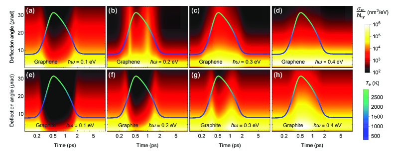
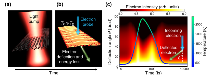
The electron signal carries spectral information on excitations in the sample, and in addition, the angular distribution of inelastically scattered electrons reveals the spatial characteristics of those excitations. The acquisition of energy-momentum-resolved maps of transmitted electrons can directly yield dispersion curves of the sample modes Pettit et al. (1975). OPEP further adds temporal resolution, as we illustrate in Figure 1. The sample (a graphene ribbon in this example) is optically pumped with an ultrafast laser (Figure 1a), which creates an elevated electronic temperature in the material that is probed at a later time by a delayed electron pulse (Figure 1a). Incidentally, the temperature rise occurs rather early because of the scaling of the electronic heat with temperature (see Appendix D). The dynamics of rapid femtosecond heating followed by the subsequent picosecond cooling of graphene electrons is traced through the delay-dependent variations observed in the distribution of scattered electrons, which is represented in Figure 1c for a fixed lost energy using the methods and analysis explained below. Additional plots analogous to Figure 1c are presented in supplementary Figure 5 for different values of the energy loss and for graphite ribbons.
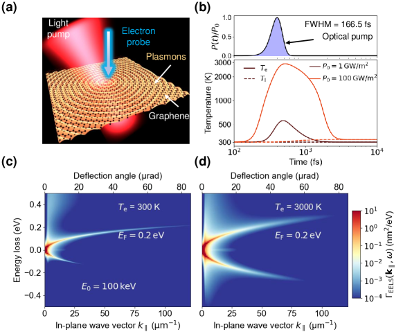
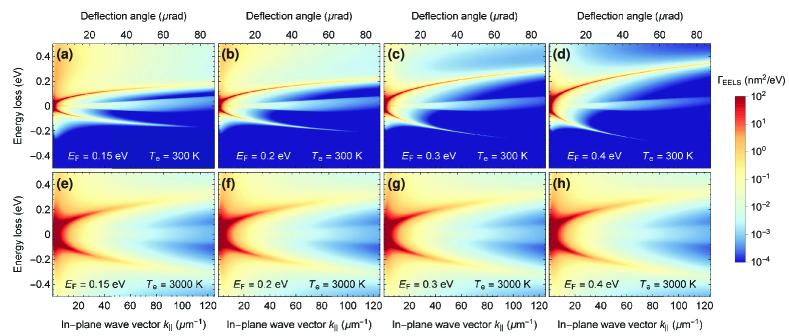
The power of momentum- and energy-resolved OPEP is illustrated in Figure 2 for a self-standing highly-doped extended graphene sample. Figure 2a shows a scheme of the pump-probe configuration, with electrons incident normal to the graphene plane. When excited by an ultrashort optical pulse, high-energy electronic bands of graphene are populated, creating a nonequilibrium distribution of hot electrons, which quickly thermalizes to a high-temperature quasistationary state due to carrier-carrier scattering George et al. (2008); Gierz et al. (2013). During a subpicosecond timescale, the electronic temperature decreases as a result of a cascade of inelastic scattering processes, in particular by emitting and absorbing phonons Hamm et al. (2016). Figure 2b shows the temporal evolution of the temperature as modelled through the two-temperature model (see details in Appendix D) for two different optical pump fluences, reaching transient electronic temperatures as high as K. When probed with a delayed quasi-monochromatic electron pulse, the graphene plasmon dispersion can be mapped out from the energy- and angle-resolved inelastically scattered electron distribution. At room temperature (Figure 2c), the dispersion relation is dominated by a plasmon band with a characteristic wave vector-frequency dispersion that is well documented for doped graphene García de Abajo (2014) (we use a Fermi energy eV throughout this paper, see Appendix A for details of the calculations). Interestingly, negative energy losses (i.e., energy gains) are observed from electrons that absorb thermally populated plasmons (Figure 2c). Energy gains associated with optical phonons were equally observed in a pioneering experiment for electrons traversing thin LiF films Boersch et al. (1966b), and more recently, this approach has been used to determine the phononic temperature in nanostructures Lagos et al. (2017); Lagos and Batson (2018). In the present study, the gain dispersion band is resolved in momentum, showing mirror symmetry with respect to the horizontal axis, except for the difference in electron scattering probability, as losses are proportional to and gains to , where is the Bose-Einstein distribution at the electron temperature (see Appendix A). At higher temperature (Figure 2d) increases, thus reducing the relative difference between gain and loss probabilities. Additionally, the plasmon energy undergoes a clearly discernible blue shift because (eV at K) exceeds eV Yu et al. (2017a). We also observe an elevation in plasmon broadening beyond the intrinsic damping (meV) due to the availability of extra electron-hole-pair transitions that become accessible as increases García de Abajo (2014). These conclusions are maintained when examining results for different values of (supplementary Figure 6) and multilayer graphene films (supplementary Figure 7). Incidentally, the fraction of inelastically scattering electrons is rather high at the relatively low plasmon energies under consideration García de Abajo (2013), giving rise to plasmon replicas associated with multiple losses (supplementary Figure 8).
II.1 Revealing lateral plasmon confinement
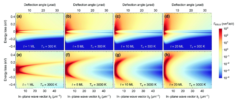
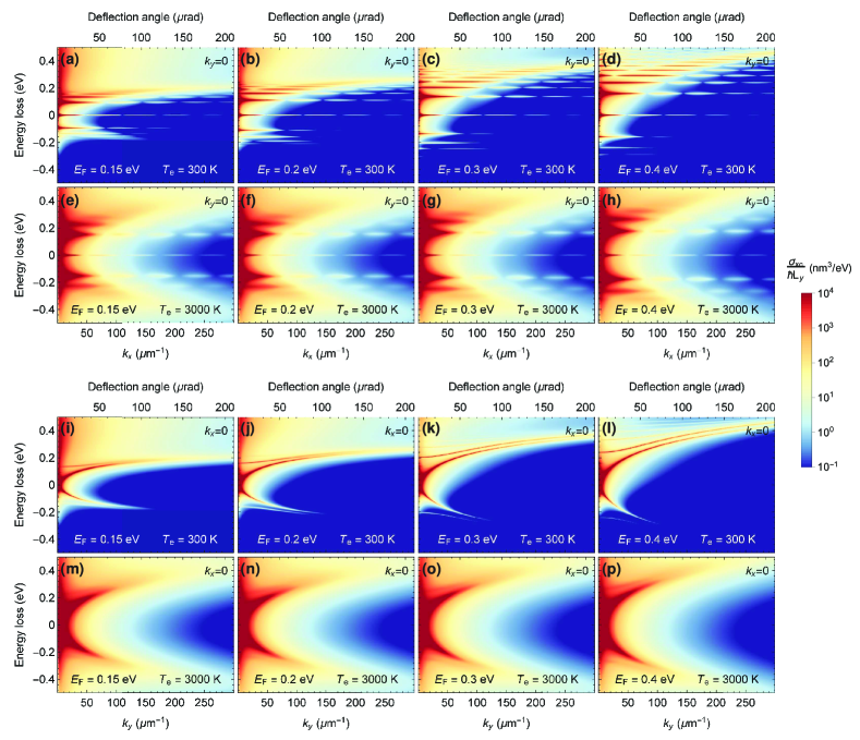
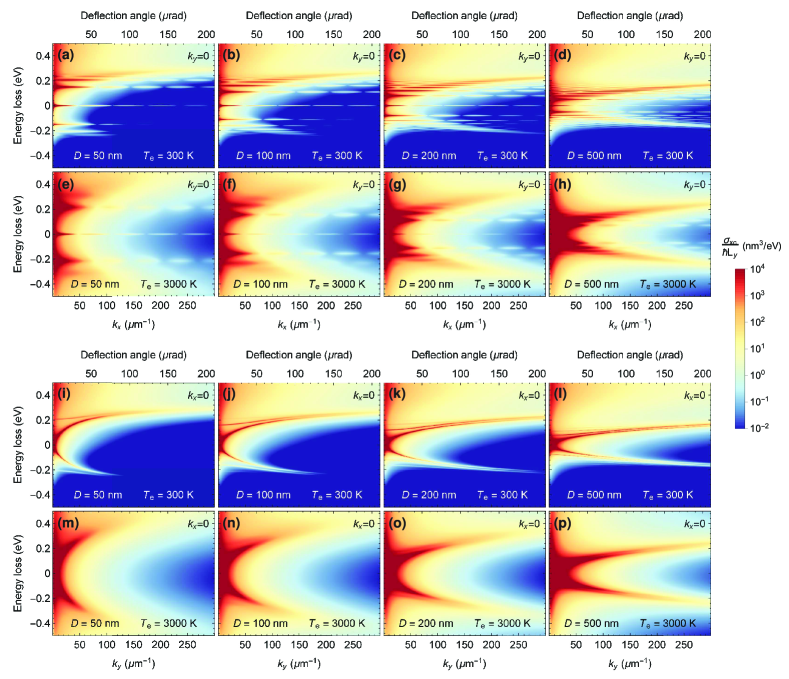
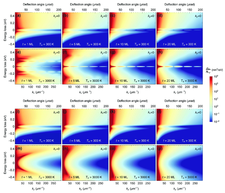
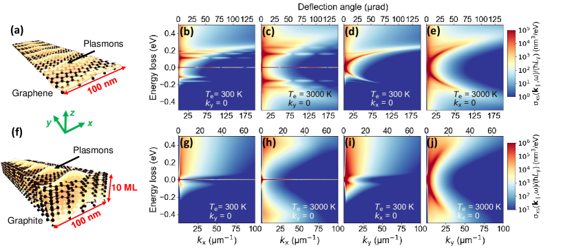
Ribbons break translational invariance and produce lateral plasmon confinement. We illustrate the resulting discretization in electron deflection in Figure 3, where the momentum- and energy-resolved inelastic scattering cross section is represented for an extended electron beam interacting with cool and heated graphene and graphite ribbons. This quantity is proportional to the loss probability, as explained in the Appendix B. In Figure 3a-e we show calculations for a 100 nm wide graphene ribbon doped to eV Fermi energy, whereas in Figure 3f-j we consider a graphite ribbon of the same width and consisting of 10 monolayers (equivalent to nm thickness) of undoped graphene (i.e., we disregard any residual doping, which should be diluted in a larger number of layers). For graphene, the results for electron deflection in the plane containing the direction of the ribbon translational symmetry (Figure 3d,e) are similar to those for planar graphene (Figure 2), as expected from the similarity between the dispersion relations of the lowest-order monopolar plasmon waveguide in ribbons (see supplementary Figure 9) and plasmons in extended samples Christensen et al. (2012). The dipolar waveguide mode, which crosses at finite energy eV, is also discernible, particularly at low temperature (Figure 3d), while higher-order modes are not efficiently excited. In contrast, electron deflection along the transverse direction (Figure 3b,c) exhibits sharp spectral features that reveal lateral confinement, accompanied by a milder momentum discretization resulting from the finite cosine-like charge distribution of plasmons across the ribbon. Like in extended graphene, an elevation in temperature produces plasmon blue shifts, an increase in spectral broadening, and a more symmetric gain-loss distribution. For graphite, the situation is different because the sample is undoped, so no plasmons are observed at low temperature (Figure 3g,i), while a broad plasmon feature emerges at 3000 K for electron deflection along the ribbon (Figure 3j), which is quantized in energy for deflection across the ribbon (Figure 3h), again due to lateral confinement. Additional plots offered in supplementary Figures 10, 11, and 12 show the variation of the results in Figure 3 with graphene doping, graphene ribbon width, and graphite thickness, respectively.
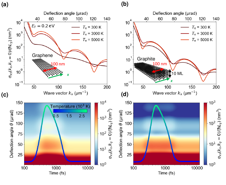
II.2 Spectrometer-free momentum-resolved OPEP
Quantization of momentum transfer due to lateral plasmon confinement suggests the possibility that these excitations and their temporal dynamics can be revealed by integrating the inelastic electron signal over a broad energy range, thus avoiding the need for highly-monochromatic electron beams and precise spectrometers. We explore this idea in Figure 4a,b, where we present the energy-integrated (within the -0.5 eV to 0.5 eV range) cross sections extracted from Figure 3 for electron deflection across the ribbon (i.e., as a function of for ). The results show clear momentum quantization in the inelastic electron signal, which becomes clearer as the temperature increases, particularly for the graphene ribbon. These observations suggest that the dynamics of the system could also be followed by measuring the energy-integrated electron angular distribution in the Fourier plane of the electron microscope. The delay-time dependence of the electron signal is shown in Figure 4c,d (density plots), following the evolution of the electronic temperature (curves) in graphene and graphite ribbons upon optical pumping. Our calculations corroborate the increase in the visibility of the oscillations observed in the inelastic scattering probability as a function of deflection angle around the time of maximum heating.
III Conclusion
Besides its fundamental interest, the study of ultrafast thermal dynamics of material excitations opens exciting opportunities for applications in optical switching and light modulation Cox and García de Abajo (2019). In this work, we have demonstrated based on solid theoretical calculations that the optical-pump/electron-probe approach, which is becoming accessible within a growing number of ultrafast electron microscope setups, grants us access into nanoscale details of such dynamics combined with femtosecond temporal resolution. This method, which brings a radical enhancement in spatial resolution compared to alternative diffraction-limited optical probes, can rely on spectrometer-free momentum-resolved electron detection (i.e., in the microscope Fourier plane) when sampling nanostructures with a well-defined characteristic length, such as the width in ribbons, leading to momentum quantization due to lateral confinement of the supported excitations. In addition, the sampled mode energies can be arbitrarily low, provided their spatial extension is small enough to produce measurable transfers of lateral momentum to the electrons. We have illustrated the power of this concept by showing that energy-integrated, angle-resolved electron signals can reveal plasmons in structures of nm lateral size, which produce electron deflection angles that are sufficiently large to be resolved by a large fraction of existing transmission electron microscopes. The proposed approach should be generally applicable to study surface excitations in 2D materials, as well as local details of insulator-metal transition in vanadium and indium-titanium oxides, where the electron and lattice dynamics triggered by pumping with ultrafast laser pulses could provide information on collective electronic and vibronic excitations with combined nanometer and femtosecond spatiotemporal resolution.
APPENDIX
Appendix A Electron energy-loss and -gain probabilities in extended planar films
We follow a well-established formalism García de Abajo (2013) to calculate the loss probability of an electron that is normally impinging on a planar thin film. The distribution of transmitted electrons as a function of transferred transverse momentum and energy is given by
at zero electronic temperature, where we disregard small retardation effects for simplicity. Here, denotes the momentum- and frequency-dependent Fresnel reflection coefficient of the film for p polarization, which is in turn expressed in terms of the surface conductivity (see Appendix C) as
where we neglect retardation effects. We thus describe the film as a zero-thickness layer under the assumption that the involved surface modes have long wavelengths compared to the film thickness. For graphene, we use the random-phase approximation (RPA) conductivity (see Appendix C), while a thin graphite film consisting of graphene planes is represented by the graphene conductivity multiplied by . For finite electronic temperature , the electron energy-loss probability needs to be corrected due to the following two effects: (1) the reflection coefficient is modified by the thermal dependence of the film conductivity (see Appendix C); and (2) the thermal population of excited electronic states in the film produces an increase in energy losses, as well as a finite probability of energy gains, captured by the expression Lucas and Šunjić (1972); Lucas and Kartheuser (1970)
where
is the frequency- and temperature-dependent Bose-Einstein distribution, the term accounts for energy gain, and we have used the property . In the present work, we apply this model to describe inelastic electron scattering in graphene and few-layer graphite extended films.
Appendix B Inelastic electron scattering cross section of planar nanostructures
We consider a free electron moving along and initially prepared in a plane wave state of energy and momentum , where and are the transverse area and longitudinal length of the quantization box, respectively. The electron is taken to interact with a planar structure lying in the plane. We aim to calculate the transition probability to a final state of energy and momentum , where is the transverse wave vector transfer and . Neglecting retardation, the energy-resolved inelastic transition rate is given by García de Abajo (2010)
where is the induced part of the screened Coulomb interaction. We now (1) make the substitution , (2) adopt the nonrecoil approximation to express the transition frequency as , where is the electron velocity, and (3) divide the rate by the incident electron current density to obtain the spectrally-resolved inelastic scattering cross section , where
| (1) |
is the cross section resolved in momentum and energy transfers and .
We describe the planar structure through a local surface conductivity . Using a quasistatic eigenmode expansion detailed elsewhere García de Abajo (2013), this allows us to express the screened interaction as
| (2) |
in terms of size-independent real-valued charge distributions and eigenvalues , where ,
| (3) |
are normalized scalar mode potentials, is the in-plane position vector normalized to the ribbon width , and labels different modes (see below). Inserting Eq. (2) into Eq. (1), we find
| (4) |
where and . Then, using the Fourier transform of the Coulomb potential in Eq. (3), we find , where
| (5) |
This allows us to recast Eq. (4) as
| (6) |
which has units of time(length)4.
Here, we apply this formalism to ribbons of width that possess translational invariance along (Figure 3a,b), so it is convenient to multiplex the mode index as into a transverse index (we retain for this purpose) and a wave vector along . This needs to be accompanied by the substitutions and , where is the ribbon length and we incorporate the wave-plane dependence on in the charge distribution. We now rewrite Eq. (5) as by making the reassignment
| (7) |
Finally, the counterpart of Eq. (6) for translationally invariant ribbons reduces to
| (8) |
which is normalized to the ribbon length and has units of time(length)3. We use Eqs. (7) and (8) to calculate the results presented in Figures 3 and 4.
Appendix C Graphene conductivity at finite temperature
The temperature-dependent nonlocal RPA surface conductivity of graphene is given by Wunsch et al. (2006); Hwang and Das Sarma (2007)
| (9) |
where the superscript 0 indicates that inelastic relaxation occurs at an infinitesimal rate, m/s is the Fermi velocity, is the electronic temperature, is the Fermi-Dirac distribution function, and is the temperature-dependent chemical potential. The latter can be approximated as Yu et al. (2017a) , where is the zero-temperature Fermi energy for a doping carrier density , and . At , we have and the conductivity admits the analytical expression Wunsch et al. (2006); Hwang and Das Sarma (2007)
with and , where the square root is taken to yield positive real parts and the imaginary part of the log function is taken in the sheet. As a more efficient alternative to evaluating the integral in Eq. (9), we calculate the -dependent conductivity from the expression using the identity Maldague (1978) , which allows us to write
Finally, we introduce a phenomenological inelastic lifetime using the Mermin prescription Mermin (1970)
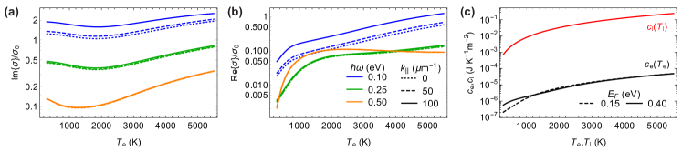
which is designed to preserve the local electron density. Although exhibits a complex dependence on temperature (see supplementary Figure 13a,b), we adopt for simplicity a constant value given by meV throughout this work. Finally, we note that we describe graphite films consisting of undoped graphene layers by means of a temperature-dependent surface-conductivity evaluated at .
Appendix D Two-temperature model
We ignore thermal diffusion under the assumption that the structures are pumped with spatially homogeneous illumination and further neglect radiative emission in our self-standing samples. Then, for simplicity, we find the time- and position-dependent electronic and lattice temperatures, and , by solving a stripped version of the two-temperature model equations Anisimov et al. (1974)
where and are the graphene electronic and phononic heat capacities per unit area, is the absorption power density due to optical pumping, and the rightmost terms account for electron-phonon coupling. We assume that the latter is dominated by disorder, which leads to the scaling Song et al. (2012); Yu et al. (2018) with , where and are the graphene mass density and deformation potential, respectively, is the graphene sound velocity, and nm. The electronic heat capacity is obtained as the derivative of the surface heat density Yu et al. (2017a) , where , where is the polylogarithm function of order . The phonon heat capacity is calculated as Benedict et al. (1996) , where m/s is the phonon velocity and is the Riemann Zeta function; this expression is valid for small compared with the Debye temperature K in graphene (see Figure 1b). Actually, is several orders of magnitude higher than (see supplementary Figure 13c), which implies that the former plays a minor role and does not increase substantially compared with (see Figure 2b).
Appendix E Summary of quasistatic eigenmodes for ribbons
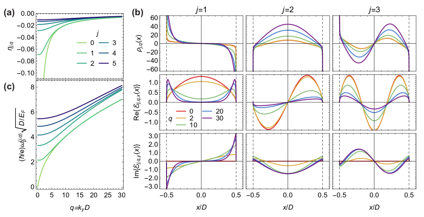
We consider a ribbon of width having translational invariance along , for which we intend to find mode eigenvalue and eigenfunctions and , where and we use the combined mode index . This problem has been addressed using different methods, including electromagnetic simulations Koppens et al. (2011), direct solution of the associated self-consistent quasistatic integral equation Shapoval et al. (2011); Tsalamengas et al. (1989), and inversion of the corresponding integral eigenvalue problem in real-space and special-function representations of the mode fields García de Abajo (2013); Khavasi and Rejaei (2014); Yu et al. (2017b); Gonçalves et al. (2020). Here, we find fast convergence in the solution of the eigenvalue problem by using a Chebyshev expansion of the electric field, as shown in detail in Appendix F, which yields the following result for the Fourier transform of the mode charge density (see Eq. (7)):
where is a Bessel function of order , and , , and (see tabulated values in supplementary Figure 9a and Tables 1 and 2) are determined from the eigensolutions of the matrix equation
| (10) |
with and (T stands for transpose). Matrices in Eq. (15) are defined in terms of blocks with coefficients
where , the indices and run from 0 to ,
is a modified Bessel function of order ,
and are Chebyshev polynomials (defined by and ), , and .
The eigenvectors and must be normalized in such a way that the mode electric fields satisfy (with ), where and
are the and components of the electric field of mode .
Appendix F Detailed derivation of a solution of quasistatic ribbon plasmon eigenfunctions through the Chebyshev expansion method
We use a Chebyshev polynomial expansion of the optical electric field to calculate semi-analytically the plasmonic eigenmodes of a graphene ribbon of width lying on the plane and having translational invariance along . The ribbon is taken to occupy the region. We describe graphene by means of a local, frequency-dependent surface conductivity and incorporate the dependence on surface position by writing , where if and 0 otherwise. The monochromatic optical electric field in the graphene plane then satisfies the integral equation García de Abajo (2013)
| (11) |
where is the average permittivity of the embedding medium (see below). Following Ref. 82, we define dimensionless coordinates and the normalized electric field to rewrite Eq. (11) as
where
and
In the absence of an external field, the above equation reduces to an eigenvalue problem:
| (12) |
Since the kernel is real and symmetric, we can find a complete set of orthonormal solutions that satisfy
where is the unit matrix.
We now focus on the specific geometry of a graphene ribbon of width . Considering its translational invariance along , we can multiplex the mode index into a normalized wave vector and the mode order for each fixed value of (we also use for the mode order). The spatial dependence of mode is thus given by
Using this, Eq. (12) can be recast as
| (13) |
where and we have made use of the identity
Now, the integral equation (13) can be written in the form
To apply the Chebyshev expansion method, it is convenient to map the integration domain onto the interval by introducing the variable changes and :
| (14) |
The essence of the Chebyshev method lies on the expansion of the kernel function in terms of the Chebyshev polynomials and , defined such that and Boyd (2001). In order to do so, we recall that the modified Bessel function can be expanded into the Neumann series Olver et al. (2010)
where is the Euler constant and denotes the modified Bessel function of order . In addition, one can use the Neumann addition formula for even-order
to represent the kernel function as a separable product of functions with arguments and . The other kernel functions in Eq. (14) can be obtained by taking the first- and second-order derivatives of the above identity with respect to :
Additionally, the modified Bessel functions can be expanded in a Chebyshev series as Wimp (1962)
with and
Using these results, we can readily expand the even-order modified Bessel functions and its derivatives in terms of Chebyshev polynomials as
where the expansion coefficients are defined as
Finally, we can obtain the Chebyshev expansion of the functions in the kernel of the integral equation in Eq. (14) as
where we have defined the quantities
It is also convenient to expand the solutions for and in terms of the Chebyshev polynomials as
which allows us to rewrite Eq. (14) in the form
Using the identities
as well as the integration properties of the Chebyshev polynomials, after some algebra, we find the results
With this notation, the integral eigenvalue problem reduces to
where we introduced the definitions
This eigenvalue problem can be recast as a generalized matrix eigenvalue problem if we choose a set of collocation points with . After doing so, we can write
| (15) |
where , (the superscript T indicates the transpose),
for , and is a zero matrix.
The eigenvalues and eigenvectors and can be readily found from Eq. (15) using standard numerical algebra methods. In general, these methods yield orthonormal eigenvectors with elements and (we add the tilde here to clarify that these are the orthonormal eigenvectors that come directly from the eigenvalue equation) that obey the property
where and (i.e., we are dealing with a fixed value of ). However, we note that it is convenient to normalize the obtained eigenvectors in a way that ensures the orthonormality conditions of the fields and . This can be done by dividing the eigenvectors and by a factor with
In this way, the orthonormality of the fields is ensured, so we have
where and .
After the expansion coefficients are found, the fields and related physical quantities can be computed analytically. We present a set of numerically obtained eigenvalues and eigenvectors in Tables 1-2 below. We also show in supplementary Figure 9 the -dependence of the first six modes of , as well as the spatial profile of the charge distribution and the associated electric fields for the first three modes and different values of . Once the eigenvectors are normalized, we can also obtain the total charge density of the mode in the ribbon as , where the -dependent function is given by
The Fourier transform of , as a function of , can finally be computed analytically, yielding
Given a certain surface conductivity of the ribbons, , we can use the obtained eigenvalues to calculate the dispersion relation of the plasmonic modes by numerically solving the equation Christensen et al. (2012)
where is the average permittivity of the materials above and below the ribbon, and we neglect inelastic losses. Considering for simplicity the Drude conductivity
defined in terms of the Fermi energy and a phenomenological inelastic decay rate , the dispersion relation admits the solution
| (16) |
We represent the resulting dispersion relations of the first six plasmon modes of the graphene ribbon in supplementary Figure 9.
Appendix G Multiple plasmon exchanges in extended films
Two-plasmon exchanges can be approximately described through the relation
| (17) |
where
| (18) |
is the single-plasmon interaction probability presented in the Methods section and involving the Bose-Einstein distribution function at the electronic temperature . The integral in Eq. (17) is computationally demanding, so we simplify it by using the plasmon-pole approximation to the reflection coefficient Dias and García de Abajo (2019)
where corresponds to the dispersion relation of the plasmons supported by the graphene sheet and is a dimensionless residue. Disregarding plasmonic losses (i.e, we take the imaginary part of to be infinitesimal), we obtain
| (19) |
Plugging Eqs. (18) and (19) into Eq. (17), we find
| (20) | ||||
The last delta function in the second line of Eq. (20) readily simplifies the integral, effectively allowing us to set . In addition, noticing that and making the change of variables , we can rewrite the remaining delta function as
with . After some straightforward algebra, we find that the two-plasmon loss probability reduces to
where
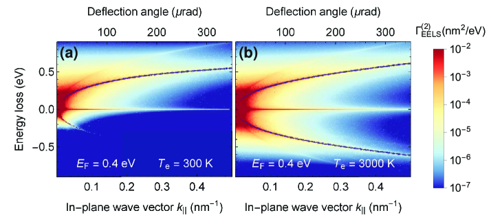
with the Heaviside function originating in the integral over , which is zero unless . We use this expression to obtain supplementary Figure 8, as it only involves a one-dimensional integral, so it is fast to compute.
| – | |||||||||
| – | |||||||||
| – | – | ||||||||
| – |
| – | – | – | – | – | |||||||
| – | – | – | – | – | – | ||||||
| – | – | – | – | – | |||||||
| – | – | – | – | – | – | ||||||
| – | – | – | – | – | |||||||
| – | – | – | – | – | – | ||||||
| – | – | – | – | – | |||||||
| – | – | – | – | – | – | ||||||
| – | – | – | – | – | |||||||
| – | – | – | – | – | – | ||||||
| – | – | – | – | – | |||||||
| – | – | – | – | – | – | – | |||||
| – | – | – | – | – | – | ||||||
| – | – | – | – | – | – | ||||||
| – | – | – | – | – | – | ||||||
| – | – | – | – | – | – | ||||||
| – | – | – | – | – | – | ||||||
| – | – | – | – | – | – | – | |||||
| – | – | – | – | – | – | ||||||
| – | – | – | – | – | – | – | |||||
| – | – | – | – | – | – | – | |||||
| – | – | – | – | – | – | – | |||||
| – | – | – | – | – | – | – | |||||
| – | – | – | – | – | – | – | – | ||||
| – | – | – | – | – | – | – | – | ||||
| – | – | – | – | – | – | – | – | ||||
| – | – | – | – | – | – | – | – |
Appendix H Acknowledgments
This work has been supported in part by the European Research Council (Advanced Grant 789104-eNANO), the Spanish MINECO (MAT2017-88492-R and SEV2015-0522), the European Commission (Graphene Flagship 696656), the Catalan CERCA Program, and Fundació Privada Cellex. F.C. acknowledges support from the ERC consolidator grant ISCQuM. E.J.C.D. acknowledges financial support from “la Caixa” (INPhINIT Fellowship Grant 1000110434, LCF/BQ/DI17/11620057) and the EU (Marie Skłodowska-Curie Grant 713673).
References
- Baffou and Quidant (2012) G. Baffou and R. Quidant, Laser Photon. Rev. 7, 171 (2012).
- Ni et al. (2016) G. X. Ni, L. Wang, M. D. Goldflam, M. Wagner, Z. Fei, A. S. McLeod, M. K. Liu, F. Keilmann, B. Özyilmaz, A. H. C. Neto, et al., Nat. Photon. 10, 244 (2016).
- Dias et al. (2020) E. J. C. Dias, R. Yu, and F. J. García de Abajo, Light Sci. Appl. 9, 87 (2020).
- Debnath et al. (2018) P. C. Debnath, S. Uddin, and Y.-W. Song, ACS Photonics 5, 445 (2018).
- Cox and García de Abajo (2019) J. D. Cox and F. J. García de Abajo, Acc. Chem. Res. 52, 2536 (2019).
- Li et al. (2014) W. Li, B. Chen, C. Meng, W. Fang, Y. Xiao, X. Li, Z. Hu, Y. Xu, L. Tong, H. Wang, et al., Nano Lett. 14, 955 (2014).
- AbdollahRamezani et al. (2015) S. AbdollahRamezani, K. Arik, S. Farajollahi, A. Khavasi, and Z. Kavehvash, Opt. Lett. 40, 5383 (2015).
- Yu et al. (2018) R. Yu, Q. Guo, F. Xia, and F. J. García de Abajo, Phys. Rev. Lett. 121, 057404 (2018).
- Kim et al. (2018) Y. D. Kim, Y. Gao, R.-J. Shiue, L. Wang, O. B. Aslan, M.-H. Bae, H. Kim, D. Seo, H.-J. Choi, S. H. Kim, et al., Nano Lett. 18, 934 (2018).
- Guo et al. (2018) Q. Guo, R. Yu, C. Li, S. Yuan, B. Deng, F. J. García de Abajo, and F. Xia, Nat. Mater. 17, 986 (2018).
- Lui and Hegmann (2001) K. P. H. Lui and F. A. Hegmann, Appl. Phys. Lett. 78, 3478 (2001).
- George et al. (2008) P. A. George, J. Strait, J. Dawlaty, S. Shivaraman, M. Chandrashekhar, F. Rana, and M. G. Spencer, Nano Lett. 8, 4248 (2008).
- Wall et al. (2012) S. Wall, D. Wegkamp, L. Foglia, K. Appavoo, J. Nag, R. F. Haglund, J. Stähler, and M. Wolf, Nat. Commun. 3, 1 (2012).
- García de Abajo (2010) F. J. García de Abajo, Rev. Mod. Phys. 82, 209 (2010).
- Kociak and Stéphan (2014) M. Kociak and O. Stéphan, Chem. Soc. Rev. 43, 3865 (2014).
- Polman et al. (2019) A. Polman, M. Kociak, and F. J. García de Abajo, Nat. Mater. 18, 1158 (2019).
- Batson et al. (2002) P. E. Batson, N. Dellby, and O. L. Krivanek, Nature 418, 617 (2002).
- Krivanek et al. (2014) O. L. Krivanek, T. C. Lovejoy, N. Dellby, T. Aoki, R. W. Carpenter, P. Rez, E. Soignard, J. Zhu, P. E. Batson, M. J. Lagos, et al., Nature 514, 209 (2014).
- Lagos et al. (2017) M. J. Lagos, A. Trügler, U. Hohenester, and P. E. Batson, Nature 543, 529 (2017).
- Hage et al. (2018) F. S. Hage, R. J. Nicholls, J. R. Yates, D. G. McCulloch, T. C. Lovejoy, N. Dellby, O. L. Krivanek, K. Refson, and Q. M. Ramasse, Sci. Adv. 4, eaar7495 (2018).
- Hage et al. (2019) F. S. Hage, D. M. Kepaptsoglou, Q. M. Ramasse, and L. J. Allen, Phys. Rev. Lett. 122, 016103 (2019).
- Hachtel et al. (2019) J. A. Hachtel, J. Huang, I. Popovs, S. Jansone-Popova, J. K. Keum, J. Jakowski, T. C. Lovejoy, N. Dellby, O. L. Krivanek, and J. C. Idrobo, Science 363, 525 (2019).
- Boersch et al. (1966a) H. Boersch, J. Geiger, A. Imbusch, and N. Niedrig, Phys. Lett. 22, 146 (1966a).
- Pettit et al. (1975) R. B. Pettit, J. Silcox, and R. Vincent, Phys. Rev. B 11, 3116 (1975).
- Chen and Silcox (1975a) C. H. Chen and J. Silcox, Phys. Rev. Lett. 35, 390 (1975a).
- Chen and Silcox (1975b) C. H. Chen and J. Silcox, Solid State Commun. 17, 273 (1975b).
- Rocca (1995) M. Rocca, Surf. Sci. Rep. 22, 1 (1995).
- Nagao et al. (2001) T. Nagao, T. Hildebrandt, M. Henzler, and S. Hasegawa, Phys. Rev. Lett. 86, 5747 (2001).
- Grinolds et al. (2006) M. S. Grinolds, V. A. Lobastov, J. Weissenrieder, and A. H. Zewail, Proc. Natl. Academ. Sci. 103, 18427 (2006).
- Barwick et al. (2008) B. Barwick, H. S. Park, O. H. Kwon, J. S. Baskin, and A. H. Zewail, Science 322, 1227 (2008).
- Barwick et al. (2009) B. Barwick, D. J. Flannigan, and A. H. Zewail, Nature 462, 902 (2009).
- Howie (1999) A. Howie, Inst. Phys. Conf. Ser. 161, 311 (1999).
- García de Abajo and Kociak (2008) F. J. García de Abajo and M. Kociak, New J. Phys. 10, 073035 (2008).
- Howie (2009) A. Howie, Microsc. Microanal. 15, 314 (2009).
- Pomarico et al. (2018) E. Pomarico, I. Madan, G. Berruto, G. M. Vanacore, K. Wang, I. Kaminer, F. J. García de Abajo, and F. Carbone, ACS Photonics 5, 759 (2018).
- García de Abajo et al. (2010) F. J. García de Abajo, A. Asenjo Garcia, and M. Kociak, Nano Lett. 10, 1859 (2010).
- Park et al. (2010) S. T. Park, M. Lin, and A. H. Zewail, New J. Phys. 12, 123028 (2010).
- Piazza et al. (2015) L. Piazza, T. T. A. Lummen, E. Quiñonez, Y. Murooka, B. Reed, B. Barwick, and F. Carbone, Nat. Commun. 6, 6407 (2015).
- Feist et al. (2015) A. Feist, K. E. Echternkamp, J. Schauss, S. V. Yalunin, S. Schäfer, and C. Ropers, Nature 521, 200 (2015).
- Lummen et al. (2016) T. T. A. Lummen, R. J. Lamb, G. Berruto, T. LaGrange, L. D. Negro, F. J. García de Abajo, D. McGrouther, B. Barwick, and F. Carbone, Nat. Commun. 7, 13156 (2016).
- Echternkamp et al. (2016) K. E. Echternkamp, A. Feist, S. Schäfer, and C. Ropers, Nat. Phys. 12, 1000 (2016).
- Priebe et al. (2017) K. E. Priebe, C. Rathje, S. V. Yalunin, T. Hohage, A. Feist, S. Schäfer, and C. Ropers, Nat. Photon. 11, 793 (2017).
- Vanacore et al. (2018) G. M. Vanacore, I. Madan, G. Berruto, K. Wang, E. Pomarico, R. J. Lamb, D. McGrouther, I. Kaminer, B. Barwick, F. J. García de Abajo, et al., Nat. Commun. 9, 2694 (2018).
- Vanacore et al. (2019) G. M. Vanacore, G. Berruto, I. Madan, E. Pomarico, P. Biagioni, R. J. Lamb, D. McGrouther, O. Reinhardt, I. Kaminer, B. Barwick, et al., Nat. Mater. 18, 573 (2019).
- Kfir et al. (2020) O. Kfir, H. Lourenço-Martins, G. Storeck, M. Sivis, T. R. Harvey, T. J. Kippenberg, A. Feist, and C. Ropers, Nature 582, 46 (2020).
- Wang et al. (2020) K. Wang, R. Dahan, M. Shentcis, Y. Kauffmann, A. B. Hayun, O. Reinhardt, S. Tsesses, and I. Kaminer, Nature 582, 50 (2020).
- Vogelgesang et al. (2018) S. Vogelgesang, G. Storeck, J. G. Horstmann, T. Diekmann, M. Sivis, S. Schramm, K. Rossnagel, S. Schäfer, and C. Ropers, NPhy 14, 184 (2018).
- Konečná et al. (2019) A. Konečná, V. Di Giulio, V. Mkhitaryan, C. Ropers, and F. J. García de Abajo, ACS Photonics 7, 1290 (2019).
- Jablan et al. (2009) M. Jablan, H. Buljan, and M. Soljačić, Phys. Rev. B 80, 245435 (2009).
- Fei et al. (2011) Z. Fei, G. O. Andreev, W. Bao, L. M. Zhang, A. S. McLeod, C. Wang, M. K. Stewart, Z. Zhao, G. Dominguez, M. Thiemens, et al., Nano Lett. 11, 4701 (2011).
- Koppens et al. (2011) F. H. L. Koppens, D. E. Chang, and F. J. García de Abajo, Nano Lett. 11, 3370 (2011).
- Chen et al. (2012) J. Chen, M. Badioli, P. Alonso-González, S. Thongrattanasiri, F. Huth, J. Osmond, M. Spasenović, A. Centeno, A. Pesquera, P. Godignon, et al., Nature 487, 77 (2012).
- Fei et al. (2012) Z. Fei, A. S. Rodin, G. O. Andreev, W. Bao, A. S. McLeod, M. Wagner, L. M. Zhang, Z. Zhao, M. Thiemens, G. Dominguez, et al., Nature 487, 82 (2012).
- Yan et al. (2012a) H. Yan, X. Li, B. Chandra, G. Tulevski, Y. Wu, M. Freitag, W. Zhu, P. Avouris, and F. Xia, Nat. Nanotech. 7, 330 (2012a).
- Yan et al. (2012b) H. Yan, Z. Li, X. Li, W. Zhu, P. Avouris, and F. Xia, Nano Lett. 12, 3766 (2012b).
- Brar et al. (2013) V. W. Brar, M. S. Jang, M. Sherrott, J. J. Lopez, and H. A. Atwater, Nano Lett. 13, 2541 (2013).
- Woessner et al. (2015) A. Woessner, M. B. Lundeberg, Y. Gao, A. Principi, P. Alonso-González, M. Carrega, K. Watanabe, T. Taniguchi, G. Vignale, M. Polini, et al., Nat. Mater. 14, 421 (2015).
- Ni et al. (2018) G. X. Ni, A. S. McLeod, Z. Sun, L. Wang, L. Xiong, K. W. Post, S. S. Sunku, B.-Y. Jiang, J. Hone, C. R. Dean, et al., Nature 557, 530 (2018).
- Lundeberg et al. (2017a) M. B. Lundeberg, Y. Gao, R. Asgari, C. Tan, B. V. Duppen, M. Autore, P. Alonso-González, A. Woessner, K. Watanabe, T. Taniguchi, et al., Science 357, 187 (2017a).
- Alcaraz Iranzo et al. (2018) D. Alcaraz Iranzo, S. Nanot, E. J. C. Dias, I. Epstein, C. Peng, D. K. Efetov, M. B. Lundeberg, R. Parret, J. Osmond, J.-Y. Hong, et al., Science 360, 291 (2018).
- Kumar et al. (2013) N. Kumar, J. Kumar, C. Gerstenkorn, R. Wang, H.-Y. Chiu, A. L. Smirl, and H. Zhao, Phys. Rev. B 87, 121406(R) (2013).
- Yao et al. (2018) B. Yao, Y. Liu, S.-W. Huang, C. Choi, Z. Xie, J. F. Flores, Y. Wu, M. Yu, D.-L. Kwong, Y. Huang, et al., Nat. Photon. 12, 22 (2018).
- Kundys et al. (2018) D. Kundys, B. V. Duppen, O. P. Marshall, F. Rodriguez, I. Torre, A. Tomadin, M. Polini, and A. N. Grigorenko, Nano Lett. 18, 282 (2018).
- Xia et al. (2009) F. N. Xia, T. Mueller, Y. M. Lin, A. Valdes-Garcia, and P. Avouris, Nat. Nanotech. 4, 839 (2009).
- Koppens et al. (2014) F. Koppens, T. Mueller, P. Avouris, A. Ferrari, M. Vitiello, and M. Polini, Nat. Nanotech. 9, 780 (2014).
- Lundeberg et al. (2017b) M. B. Lundeberg, Y. Gao, A. Woessner, C. Tan, P. Alonso-González, K. Watanabe, T. Taniguchi, J. Hone, R. Hillenbrand, and F. H. L. Koppens, Nat. Mater. 16, 204 (2017b).
- Yuan et al. (2020) S. Yuan, R. Yu, C. Ma, B. Deng, Q. Guo, X. Chen, C. Li, C. Chen, K. Watanabe, T. Taniguchi, et al., ACS Photonics 7, 1206 (2020).
- Rodrigo et al. (2015) D. Rodrigo, O. Limaj, D. Janner, D. Etezadi, F. J. García de Abajo, V. Pruneri, and H. Altug, Science 349, 165 (2015).
- Hu et al. (2016) H. Hu, X. Yang, F. Zhai, D. Hu, R. Liu, K. Liu, Z. Sun, and Q. Dai, Nat. Commun. 7, 12334 (2016).
- Hu et al. (2019) H. Hu, X. Yang, X. Guo, K. Khaliji, R. Biswas, F. J. García de Abajo, T. Low, Z. Sun, and Q. Dai, Nat. Commun. 10, 1131 (2019).
- García de Abajo (2014) F. J. García de Abajo, ACS Photonics 1, 135 (2014).
- Gao et al. (2015) Y. Gao, R.-J. Shiue, X. Gan, L. Li, C. Peng, I. Meric, L. Wang, A. Szep, D. W. Jr., J. Hone, et al., Nano Lett. pp. 2001–2005 (2015).
- Vafek (2006) O. Vafek, Phys. Rev. Lett. 97, 266406 (2006).
- Jadidi et al. (2016) M. M. Jadidi, J. C. König-Otto, S. Winnerl, A. B. Sushkov, H. D. Drew, T. E. Murphy, and M. Mittendorff, Nano Lett. 16, 2734 (2016).
- Johannsen et al. (2013) J. C. Johannsen, S. Ulstrup, F. Cilento, A. Crepaldi, M. Zacchigna, C. Cacho, I. C. E. Turcu, E. Springate, F. Fromm, C. Raidel, et al., Phys. Rev. Lett. 111, 027403 (2013).
- Gierz et al. (2013) I. Gierz, J. C. Petersen, M. Mitrano, C. Cacho, I. C. E. Turcu, E. Springate, A. Stöhr, A. Köhler, U. Starke, and A. Cavalleri, Nat. Mater 12, 1119 (2013).
- Nair et al. (2008) R. R. Nair, P. Blake, A. N. Grigorenko, K. S. Novoselov, T. J. Booth, T. Stauber, N. M. R. Peres, and A. K. Geim, Science 320, 1308 (2008).
- Hamm et al. (2016) J. M. Hamm, A. F. Page, J. Bravo-Abad, F. J. Garcia-Vidal, and O. Hess, Phys. Rev. B 93, 041408 (2016).
- Boersch et al. (1966b) H. Boersch, J. Geiger, and W. Stickel, Phys. Rev. Lett. 17, 379 (1966b).
- Lagos and Batson (2018) M. J. Lagos and P. E. Batson, Nano Lett. 18, 4556 (2018).
- Yu et al. (2017a) R. Yu, A. Manjavacas, and F. J. García de Abajo, Nat. Commun. 8, 2 (2017a).
- García de Abajo (2013) F. J. García de Abajo, ACS Nano 7, 11409 (2013).
- Christensen et al. (2012) J. Christensen, A. Manjavacas, S. Thongrattanasiri, F. H. L. Koppens, and F. J. García de Abajo, ACS Nano 6, 431 (2012).
- Lucas and Šunjić (1972) A. A. Lucas and M. Šunjić, Progr. Surf. Sci. 2, 75 (1972).
- Lucas and Kartheuser (1970) A. A. Lucas and E. Kartheuser, Phys. Rev. B 1, 3588 (1970).
- Wunsch et al. (2006) B. Wunsch, T. Stauber, F. Sols, and F. Guinea, New J. Phys. 8, 318 (2006).
- Hwang and Das Sarma (2007) E. H. Hwang and S. Das Sarma, Phys. Rev. B 75, 205418 (2007).
- Maldague (1978) P. F. Maldague, Surf. Sci. 73, 296 (1978).
- Mermin (1970) N. D. Mermin, Phys. Rev. B 1, 2362 (1970).
- Anisimov et al. (1974) S. I. Anisimov, B. L. Kapeliovich, and T. L. Perel’man, J. Exp. Theor. Phys. 41, 375 (1974).
- Song et al. (2012) J. C. W. Song, M. Y. Reizer, and L. S. Levitov, Phys. Rev. Lett. 109, 106602 (2012).
- Benedict et al. (1996) L. X. Benedict, S. G. Louie, and M. L. Cohen, Solid State Commun. 100, 177 (1996).
- Shapoval et al. (2011) O. V. Shapoval, R. Sauleau, and A. I. Nosich, IEEE Trans. Antennas Propag. 59, 3339 (2011).
- Tsalamengas et al. (1989) J. L. Tsalamengas, J. G. Fikioris, and B. T. Babili, J. Appl. Phys. 66, 69 (1989).
- Khavasi and Rejaei (2014) A. Khavasi and B. Rejaei, IEEE J. Quantum Electron. 50, 397 (2014).
- Yu et al. (2017b) R. Yu, J. D. Cox, J. R. M. Saavedra, and F. J. García de Abajo, ACS Photonics 4, 3106 (2017b).
- Gonçalves et al. (2020) P. A. D. Gonçalves, N. Stenger, J. D. Cox, N. A. Mortensen, and S. Xiao, Adv. Opt. Mater. 8, 1901473 (2020).
- Boyd (2001) J. P. Boyd, Chebyshev and Fourier spectral methods (Courier Corporation, New York, 2001).
- Olver et al. (2010) F. W. J. Olver, D. W. Lozier, R. F. Boisvert, and C. W. Clark, NIST Handbook of Mathematical Functions Hardback and CD-ROM (Cambridge University Press, New York, 2010).
- Wimp (1962) J. Wimp, Math. Comput. 16, 446 (1962).
- Dias and García de Abajo (2019) E. J. C. Dias and F. J. García de Abajo, ACS Nano 13, 5184 (2019).
Appendix I Supplementary Figures