Electronic properties of InAs/EuS/Al hybrid nanowires
Abstract
We study the electronic properties of InAs/EuS/Al heterostructures as explored in a recent experiment [S. Vaitiekėnas et al., Nat. Phys. (2020)], combining both spectroscopic results and microscopic device simulations. In particular, we use angle-resolved photoemission spectroscopy to investigate the band bending at the InAs/EuS interface. The resulting band offset value serves as an essential input to subsequent microscopic device simulations, allowing us to map the electronic wave function distribution. We conclude that the magnetic proximity effects at the Al/EuS as well as the InAs/EuS interfaces are both essential to achieve topological superconductivity at zero applied magnetic field. Mapping the topological phase diagram as a function of gate voltages and proximity-induced exchange couplings, we show that the ferromagnetic hybrid nanowire with overlapping Al and EuS layers can become a topological superconductor within realistic parameter regimes, and that the topological phase can be optimized by external gating. Our work highlights the need for a combined experimental and theoretical effort for faithful device simulations.
I Introduction
Topological superconductivity (TSC) has attracted lots of attention and inspired intensive research over the last few decades. The defects or wire ends of a TSC can host Majorana zero modes which are non-Abelian anyons and potential building blocks of topological quantum computing Nayak et al. (2008); Alicea (2012); Leijnse and Flensberg (2012); Beenakker (2013); Stanescu and Tewari (2013); Jiang and Wu (2013); Elliott and Franz (2015); Sarma et al. (2015); Sato and Fujimoto (2016); Sato and Ando (2017); Aguado (2017); Lutchyn et al. (2018); Zhang et al. (2019); Frolov et al. (2020). Heterostructures between a spin-orbit coupled semiconducting nanowire and a conventional -wave superconductor is one of the promising platforms for realizing TSC Sau et al. (2010a); Lutchyn et al. (2010); Oreg et al. (2010); Sau et al. (2010b). In these hybrid devices, topological superconductivity is realized for a sufficiently strong Zeeman splitting.
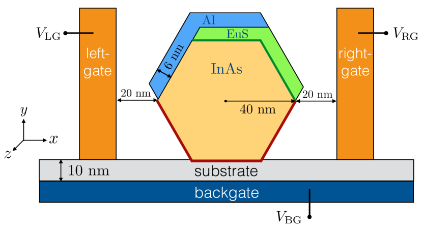
In most experimental studies of semiconductor-superconductor hybrid nanowires so far, Zeeman splitting is induced by an externally applied magnetic field Mourik et al. (2012); Das et al. (2012); Deng et al. (2012); Churchill et al. (2013); Finck et al. (2013); Albrecht et al. (2016); Chen et al. (2017); Deng et al. (2016); Zhang et al. (2017); Gül et al. (2018); Nichele et al. (2017). However, Zeeman energy in the hybrid system can also be induced by proximity effect from ferromagnetic insulators (FMI) Sau et al. (2010a, b). In a recent experiment, topological properties of InAs/EuS/Al ferromagnetic (FM) hybrid nanowires have been investigated Vaitiekėnas et al. (2020). Tunneling spectroscopy revealed zero-bias conductance peaks over a finite parameter regime for multiple devices, compatible with Majorana zero modes and topological superconductivity. Interestingly, such zero-bias peaks have appeared only in devices of a particular geometry, namely when the Al and EuS layers overlap with each other by one facet (see Fig. 1), but not in other device geometries without such an overlap. This raises the question on the fundamental physical mechanisms for realizing TSC in such ferromagnetic hybrid nanowires.
In this work, we explore systematically different mechanisms for inducing an effective Zeeman energy in the nanowire, using detailed microscopic device simulations. To this end it is essential to have a faithful description of the electrostatic potential in the device. Previous works highlighted the critical role of band offsets at interfaces of the semiconductor with other materials Antipov et al. (2018); Mikkelsen et al. (2018). For the bare InAs surface and the InAs/Al interface this has been studied systematically using angle-resolved photoemission spectroscopy (ARPES) Schuwalow et al. (2019), but no such analysis has been available for the InAs/EuS interface so far.
We combine an analysis of the band offset at the InAs/EuS interface from ARPES data with electrostatic device simulations to arrive at a faithful description of the electronic density in these hybrid nanowires. In particular, we find that the enhanced band bending at the InAs/EuS interface leads to an accumulation of electrons along these facets. Using a microscopic model for superconductivity we conclude that the magnetic proximity effects at the Al/EuS as well as the InAs/EuS interfaces are both essential for inducing a sufficiently large effective Zeeman spin splitting allowing to reach a topological phase. Our calculations show that a topological phase can be reached with plausible parameter values, and we discuss how topological properties can be optimized by external gating.
II Band bending and Electrostatics
II.1 Band bending at the InAs/EuS interface
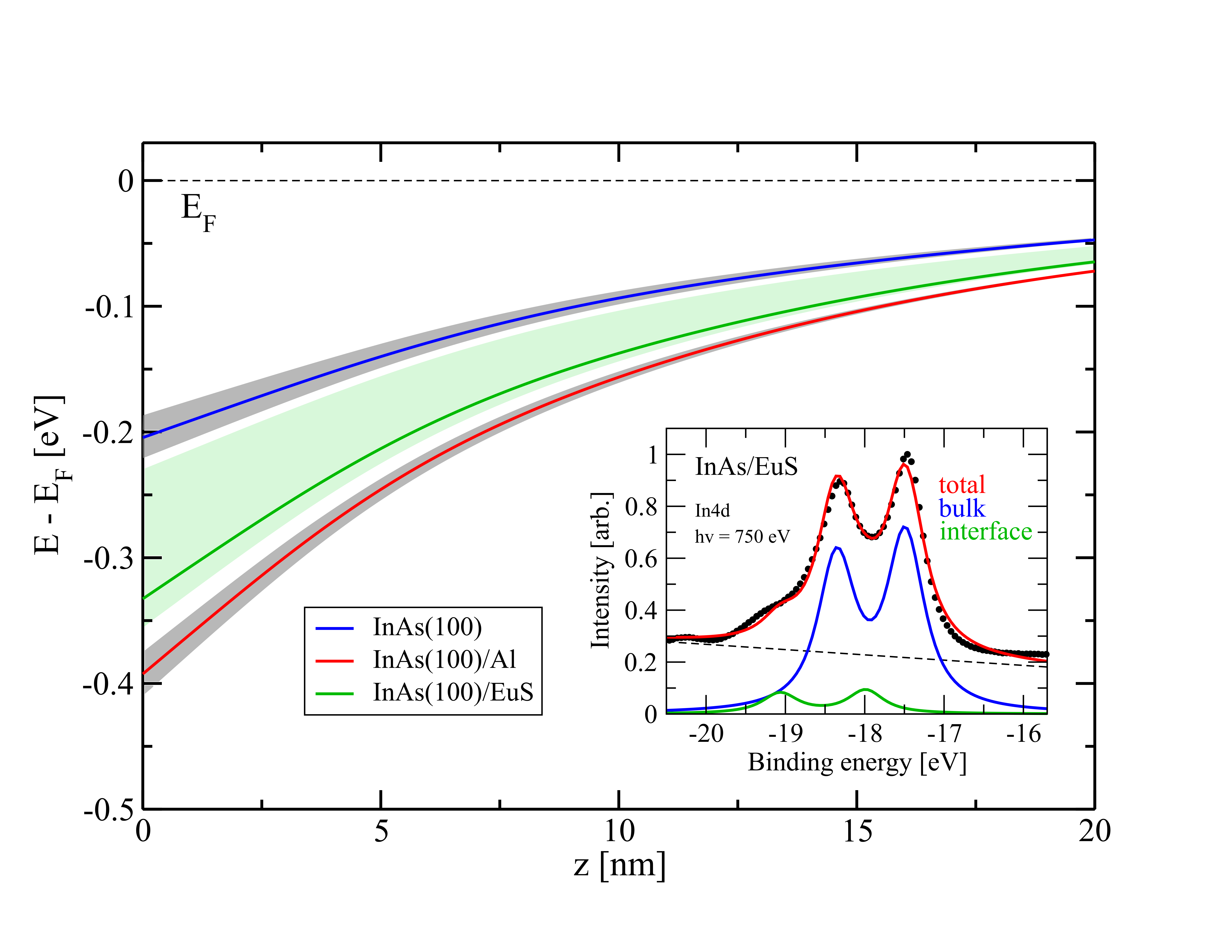
Accurate values of band offset at the interface of InAs with other materials are crucial for obtaining faithful electrostatic potential and charge density profiles inside the InAs nanowire. In a previous work Schuwalow et al. (2019), the planar interfaces of InAs/Al and InAs/vacuum were both carefully investigated using the ARPES measurements along with the core-level fitting procedure. The resulting values of the band offset of InAs(100)/Al and InAs(100)/vacuum, and the band bending profile near the interface are summarized as the blue and red lines in Fig. 2 (data from Ref. Schuwalow et al. (2019)).
In this work, we focus on the band bending effect at the InAs(100)/EuS interface. ARPES data obtained for this interface has been presented in Ref. Liu et al. (2020a). Here, we use the methods described in Ref. Schuwalow et al. (2019) to extract the band bending from this data. In particular, the fit of the In4d core-level spectra for the InAs/EuS interface is performed simultaneously for a set of photon energies in the range 350-750 eV. We use a bulk and an interface component consisting of two Voigt functions each. The broadening and shift of the line profile by the band bending potential is accounted for using an auxiliary Schrödinger-Poisson simulation and the characteristic energy between the conduction band minimum and the In4d core level eV for InAs Schuwalow et al. (2019).
The result of the core-level fitting for = 750 eV is shown in the inset of Fig. 2. While the overall shape of the core line is well captured by our model, the bulk component binding energy seems to be underestimated by 0.08 eV. We suspect that this may be caused by nonlinear behavior of the background or by a small additional interface component that is not adequately captured in our approach, which is reflected in the increased estimate for the confidence interval towards lower binding energies. The bend bending profile of InAs(100)/EuS interface is shown as the green line in Fig. 2, and we see that the band offset value of InAs/EuS is in between the values of InAs/Al and InAs/vacuum.
Finally, we note that owing to the geometrical difference between a planar interface and a multi-facet nanowire structure, the band offset values shown in Fig. 2 should be regarded as guiding values. For the InAs/Al interface specifically, we typically observe the value of band offset for in-situ planar MBE growth shown here to be an upper bound, with a reduction of 0.05-0.1 eV for interfaces with a reduced quality using other growth modes such as growth after decapping. We can expect this to apply to growth on nanowire facets. So without loss of generality, in this work we choose the band offset values in our model to be 0.2 eV, 0.26 eV and 0.35 eV, respectively.
II.2 Thomas Fermi-Poisson approach
The setup for studying the electrostatics in this work is schematically shown in Fig. 1. We focus on the two-dimensional cross section (in the - plane) of the system, and assume translational symmetry along the third dimension ( axis). The hexagonal InAs nanowire of radius 40 nm is covered by the EuS layer on two of the top facets, and also covered by the Al layer on one adjacent facet. The hybrid nanowire is placed on a dielectric layer of thickness 10 nm, and a back-gate and two side-gates are applied below or beside the nanowire. To obtain the electrostatic potential for the setup, we solve the self-consistent Thomas Fermi-Poisson equation Vuik et al. (2016); Antipov et al. (2018); Mikkelsen et al. (2018); Woods et al. (2018); Winkler et al. (2019); Armagnat et al. (2019)
| (1) |
with appropriate boundary conditions. Here the total charge density
| (2) |
includes the conduction electrons, the heavy/light holes, and the surface charges. We use the Thomas-Fermi approximation for a 3D electron gas to determine the mobile charge densities inside the InAs nanowire:
| (3) |
where , , are the effective mass of the conduction electron, the heavy-hole and the light-hole in unit of electron mass, eV is the band gap between conduction and valence bands Winkler et al. (2003), and is the Heaviside step function. The surface charges are added to account for the band bending effect at both InAs/EuS and InAs/vacuum interfaces. At the two top facets of the InAs nanowire, where it is in contact with the EuS layer, a positive charge layer of 1 nm thickness and density is added, leading to a band offset eV. Similarly, at the three facets where the InAs nanowire is either in contact with vacuum or the dielectric layer, another 1 nm thick positive charge layer of density is applied to model the band offset value eV Olsson et al. (1996); Degtyarev et al. (2017); Winkler et al. (2019); Woods et al. (2020). The band bending effect at the interface of InAs and the metallic aluminum layer is modeled by the Dirichlet boundary condition, i.e., V at the remaining one facet of the InAs nanowire. Additionally, the regions of the gates are also Dirichlet boundary conditions, with the values being determined by the applied voltage value, i.e., , BG, LG, and RG. It is noteworthy that the treatment of the band bending effect at the InAs/EuS interface is unique to this work, and thus distinguishes our work from others Woods and Stanescu (2020)
III Electronic properties of ferromagnetic hybrid nanowires
| Table I. Physical parameters for InAs and Al | ||
| Parameter (unit) | InAs | Al |
| m () | 0.023 Winkler et al. (2003) | 1 |
| (eVÅ) | 0.3 Gmitra and Fabian (2016) | 0 |
| (eV) | 0 | 11.27 Cochran and Mapother (1958) |
| (meV) | 0 | 0.34 Cochran and Mapother (1958) |
| 15.15 | ||
III.1 Model Hamiltonian
The quantum model for investigating the electronic properties of the hybrid nanowire is shown in Fig. 1. We consider the two-dimensional cross section of the nanowire (-plane), assuming translational symmetry along the wire axis (-axis). The quantum system consists of only the InAs nanowire and the Al layer, which we treat on equal footing at the quantum mechanical level. We model the role of EuS as an induced exchange coupling term in InAs and Al, while neglecting the stray field from EuS Liu et al. (2020b). The effects of gates, surface charges, dielectric layers, and the vacuum are taken into account via the self-consistently calculated electrostatic potential inside the InAs nanowire. Under these assumptions, the normal-state Hamiltonian for the ferromagnetic hybrid nanowire can be written as
| (4) |
where is the momentum operator with being the Planck constant, the wave vector along the nanowire axis, the Pauli matrices acting on the spin space, the effective mass, the strength of the Rashba spin-orbit coupling, the Fermi energy, the electrostatic potential, the elementary charge, and the strength of the induced exchange coupling due to the magnetic proximity effect from EuS. The physical parameters for InAs and Al are summarized in Table I. In addition, a random onsite potential is added within a distance of nm from the outer surface of Al, modeling the effect of disorder induced by the amorphous oxide layer in realistic devices Antipov et al. (2018). We assume that the disorder potential has strength eV with zero average, and is spatially uncorrelated, i.e., , , such that the bands in Al and InAs couple to each other strongly Antipov et al. (2018); Winkler et al. (2019).
When superconductivity is taken into consideration, the system is described by the Bogoliubov-de Gennes (BdG) Hamiltonian
| (5) |
in the basis of . Here are the Pauli matrices acting on the Nambu space, and is the pairing potential in the superconductor.
For the numerical calculations, the Hamiltonians in Eqs. (4) and (5) are first discretized into a tight-binding model on a square lattice using the KWANT package Groth et al. (2014). We choose the lattice constants for InAs and Al to be 5 Å and 1 Å, respectively, to account for the large Fermi energy difference between the two materials. Then the eigenenergies and eigenstates are obtained by diagonalizing the sparse Hamiltonian matrices.
III.2 Exchange coupling in Al
We first investigate the effect of induced exchange coupling inside the aluminum layer on the electronic properties of the InAs/Al hybrid system. The origin of this exchange coupling is the magnetic proximity effect between the Al and EuS layers when they overlap with each other, as indicated in the schematic of Fig. 1. To model this proximity effect, we assume that inside the Al layer. At this point we still neglect the magnetic proximity effect at the InAs/EuS interface; this will be discussed in the next section.
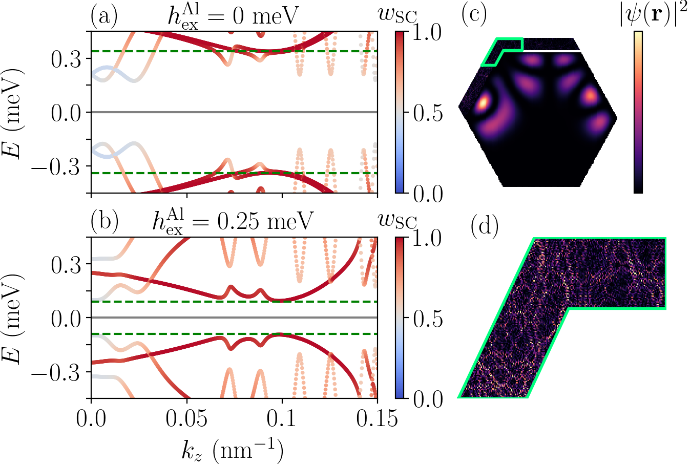
Figures 3(a) and 3(b) show the BdG band diagrams of the InAs/Al hybrid system in the absence ( = 0 meV) and presence ( = 0.25 meV) of the induced exchange coupling in Al, with the gate voltages being fixed at V and V. The color of the band indicates the degree of wavefunction hybridization, which is defined as , with denoting the volume of the Al layer. A finite has two effects on the band properties of the hybrid nanowire.
First, a finite would induce an effective Zeeman spin slitting for the hybrid state. As can be seen, the spin-orbit degeneracy at and meV in Fig. 3(a) for the hybrid state () is now lifted by the finite induced exchange coupling in Al in Fig. 3(b). The amplitude of the effective Zeeman energy is approximately
| (6) |
which is proportional to the weight of the wavefunction in Al. Figures 3(c) and 3(d) show the wavefunction profiles of the hybrid state in InAs and Al, respectively. Thereby, although InAs is not directly subject to the magnetic proximity effect from EuS in the physical scenario considered here, the hybrid state still gains a finite effective Zeeman spin splitting by distributing its wavefunction into the magnetized Al layer.
Second, the induced exchange coupling in Al would reduce the quasiparticle continuum gap. By comparing those superconducting states () in Figs. 3(a) and 3(b), we find that the excitation gap of the Al layer decreases from the bare value meV to about meV [green dashed lines in Figs. 3(a) and 3(b)]. Since Al is an -wave BCS superconductivity, the quasiparticle continuum gap decreases with the induced exchange coupling in Al in a linear manner:
| (7) |
Thus we can estimate the strength of induced exchange coupling from experimental data by considering the reduction of the quasiparticle continuum gap in Al. On the other hand, for the hybrid state (), the excitation gap (inverse of the localization length of the Majorana modes) at in Figs. 3(a) and 3(b) changes very little with , possibly owing to the spin-orbit protection from InAs Bommer et al. (2019); Liu et al. (2019).
When considering both of the abovementioned two effects on the InAs/Al hybrid nanowire, we conclude that an induced exchange coupling in Al alone cannot drive the hybrid system into the topological phase. Because by combining Eqs. (6) and (7), the induced effective Zeeman energy of the hybrid state is always less than the induced superconducting gap, i.e.,
| (8) |
as long as the quasiparticle continuum gap in Al remains finite . This is in agreement with a fundamental no-go theorem for topology for BdG Hamiltonians et al. .
III.3 Direct magnetic proximity effect
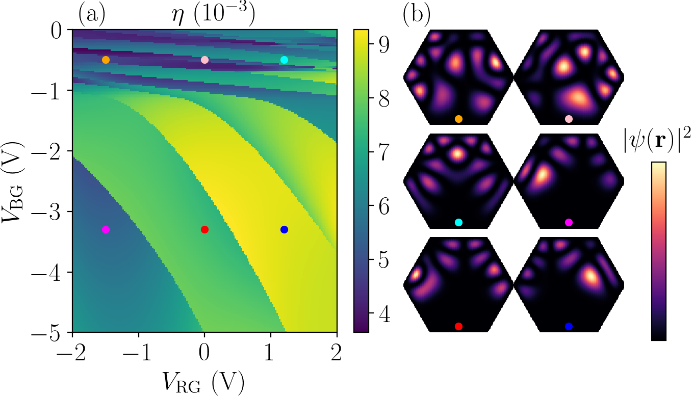
We now focus on the direct magnetic proximity effect at the InAs/EuS interface and its dependence on gates, neglecting the superconducting shell completely. In particular for the quantum problem, we consider a bare InAs nanowire and the direct proximity effect is modeled phenomenologically as a local exchange coupling within a distance nm from the two-facet boundaries where InAs and EuS contact with each other. Here, the distance is chosen to be about the penetration length of the wavefunction in a typical magnetic insulator Sau et al. (2010b), such that the magnitude of can be approximated as the strength of the ferromagnetic coupling inside EuS. We have chosen for this phenomenological approach as the band structure of EuS may not be represented faithfully with an effective mass model as used for InAs and Al in our study. The effect of the back-gate and two side-gates is included via the electrostatic potential profile , which is calculated based on the geometry shown in Fig. 1. In order to quantify the magnetic proximity effect, we define the efficiency , which is the Zeeman energy splitting of the -th spinful subband in the presence of a unit-strength . is the energy eigenstate of the discretized normal Hamiltonian in Eq. (4).
Figure 4(a) shows the calculated of the normal subband mode closest to the Fermi surface as a function of the backgate and rightgate voltages (the leftgate dependence is weak due to the screening effect of Al). The efficiency is a piecewise function of the gate voltages, with each piece corresponding to a particular subband mode. The difference between distinct subband modes can be stark and dominates the variations within a single subband mode. Note that although the dependence of on the gate voltages is not monotonic, a general trend is that the subband mode at a more negative (positive) value of the backgate (rightgate) voltage would have a larger , because their wavefunctions are more confined towards the InAs/EuS interface where the direct magnetic proximity effect is the strongest, as shown in Fig. 4(b).
The generalization from the bare InAs to the InAs/Al hybrid nanowire is straightforward. Namely, the effective Zeeman splitting for the hybrid state due to the direct magnetic proximity effect can be approximated as
| (9) |
where the prefactor accounts for the semiconductor-superconductor hybridization. In the absence of other mechanisms of inducing Zeeman splitting, the minimal strength of the exchange coupling for realizing TSC would be about by requiring . For a typical device with strong coupling at both InAs/Al and InAs/EuS interfaces, e.g., and [see Fig. 4(a)], we have meV. Such a large strength of exchange coupling sets a demanding requirement for the proximity magnetic insulator candidates.
III.4 Topological phase diagram
We now consider the scenario in which the InAs/Al hybrid nanowire is subject to the joint magnetic proximity effect from both Al/EuS and InAs/EuS interfaces, and study the topological phase diagrams as a function of gate voltages and exchange couplings. Namely, the induced exchange coupling is finite both in Al and at the boundaries of InAs, and thereby the total effective Zeeman spin splitting now is the combined contribution of two mechanisms:
| (10) |
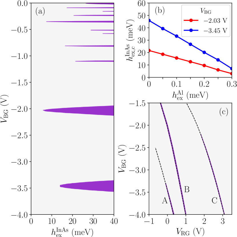
where and are estimated in Eqs. (6) and (9). To determine the topological phase diagram of the hybrid nanowire, we keep track of the energy gap . For semiconductor-superconductor nanowires, the closing and reopening of signifies the topological quantum phase transition Sau et al. (2010a); Lutchyn et al. (2010); Oreg et al. (2010); Sau et al. (2010b). Figure 5(a) shows the topological phase diagram of the device in Fig. 1 as a function of the backgate voltage and the exchange coupling in InAs, with other parameters being fixed at meV, and V. The areas in purple represent the topological phase of the nanowire, while those in grey represent the trivial phase. There are several observations on the result in Fig. 5(a). First, the pattern of the phase diagram resembles those of the hybrid nanowires for which the Zeeman energy is induced by an applied magnetic field but without including the orbital effect from the field. Because in our model, the Zeeman energy is induced by the exchange couplings at zero magnetic field. Second, the TSC phases (lobes in purple) at V are more robust, based on the fact that they have a smaller critical exchange coupling strength, and a larger width along . The robustness is the consequence of the joint effect of a larger direct magnetic proximity effect ( as shown in Fig. 4) and a stronger InAs/Al hybridization ( as shown in Fig. 3) at more negative gate voltages. Third, the minimal strength of the critical exchange field for achieving topological phases is about 10 meV for the two lobes at V and V. Such a strength of at the InAs/EuS interface is comparable to the estimated strength of exchange coupling at the interface of III-V compounds and magnetic insulators, which confirms the feasibility to realize TSC in semiconductor-superconductor-ferromagnetic hybrid nanowires with overlapping Al and EuS layers. This is one of the central result in the current work.
Figure 5(b) shows the minimally required strength of at the InAs/EuS interface as a function of in Al for two particular subband modes. The minimal strength decreases linearly with an increasing , because an larger effective Zeeman energy facilitates the realization of topological superconductivity in the hybrid nanowire. In particular, the minimally required exchange coupling at the InAs/EuS interface is about 50 or 20 meV if no exchange coupling is induced in Al. This value reduces significantly to 10 or 5 meV as meV. Here for comparison between theory and experiment, the value of is chosen such that the shrinking of the continuum gap is comparable to the observations in Ref. Vaitiekėnas et al. (2020), i.e., the gap in devices with overlapping Al and EuS layers is of the gap in non-overlapping ones. If we assume that the properties of a hybrid nanowire with non-overlapping Al and EuS layers are approximately captured by setting in our model, Fig. 5(b) explains why zero-bias conductance peaks in the tunnel spectroscopy are only observed in overlapping devices in Ref. Vaitiekėnas et al. (2020).
Figure 5(c) shows the topological phase diagram in the (, ) plane, focusing on the three topological lobes at V. Now the exchange couplings are fixed at meV and meV, and gate voltages . The topological phase shows up as a diagonal line, along which the Fermi energy of the relevant subband mode keeps close to zero. Note that the hybrid state of the particular subband mode can remain topological all the way along the diagonal zero-Fermi-energy line (e.g., the continuous lobe-B), or it can transform between topologically trivial and nontrivial phases (e.g., lobes-A or -C). It turns out that the topology along the zero-Fermi-energy line depends crucially on how the semiconductor-superconductor hybridization () and direct magnetic proximity efficiency () respond to the gate voltage variations. For the hybrid state with zero Fermi energy, we can use a simplified criterion in the form
| (11) |
based on the definitions in Eqs. (6), (8), (9) and (10). In Eq. (11), the relative strength of Zeeman energy due to the direct magnetic proximity effect and the induced quasiparticle continuum gap depend on and explicitly.
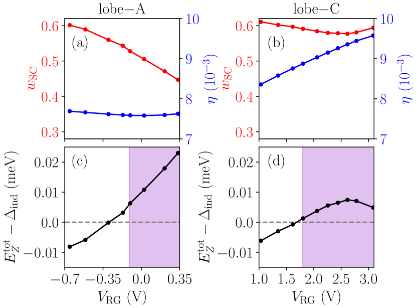
Figure 6 shows the and of the lobes-A and -C along the zero-Fermi-energy line, i.e., the dashed lines in Fig. 5(c). In Fig. 6(a), the variation of dominates that of , and the hybrid state is topological [see Fig. 6(c)] when the hybridization is moderately small, i.e., . As indicated by Eq. (11), a smaller degree of semiconductor-superconductor hybridization means a stronger from the InAs side and a smaller induced continuum gap from Al, making it easier to satisfy the topological criterion. In another scenario, as shown by Fig. 6(b) for lobe-C, increases monotonically as the voltage of the right-gate becomes more positive, and has a dominant effect than . The hybrid state becomes topological when is sufficiently large. We thus see that depending on the details of a subband, a topological transition can be driven by two gates by both changing the induced superconducting gap or the directly induced Zeeman splitting. This is in contrast to the usual topological phase transition driven by changing the chemical potential by a gate.
IV Summary and discussions
In this work, we studied the electronic properties of InAs/EuS/Al hybrid nanowires. We analyzed the band bending at the InAs/EuS interface using ARPES data and found that this interface enhances electron accumulation compared to a bare InAs surface. Using this input, we performed microscopic electrostatics and device simulations. From these we concluded that it is feasible to achieve topological superconductivity in the device geometry shown in Fig. 1, within the realistic parameters: the calculated minimal strength of at the InAs/EuS interface is about meV, consistent with the induced exchange coupling between III-V semiconductors and magnetic insulators. Our calculations also indicate that in experiments a topological phase is only achieved by the combination of both an induced Zeeman splitting in the superconducting Al shell by EuS, and an induced Zeeman splitting directly at the InAs/EuS interface. We also find in this hybrid device additional ways to control the topological phase by gates compared to the well-known control by changing the chemical potential: Topology can be controlled using two gates either by changing the effective induced superconducting gap or by changing the overlap of the wave function with the InAs/EuS interface and thus the directly induced Zeeman splitting. This gives new avenues to experimentally optimizing topological phases in a given device geometry.
While finishing this work we became aware of a similar study on InAs/EuS/Al nanodevices focusing on electrostatic effects Woods and Stanescu (2020). That work concludes, opposite to our findings, that only the directly induced Zeeman splitting is necessary for a topological phase. The reason for this discrepancy is that Ref. Woods and Stanescu (2020) only assumes electron accumulation due to the work function difference between Al and InAs, and not at the InAs/EuS interface, contrary to our experimental finding. We note that there is concurrent work on the effects of electrostatics in these hybrid systems Yeyati and Prada . Also, there are concurrent efforts to go beyond the effective model as used in our work, and do a self-consistent treatment of proximity effect between EuS and Al when the shells overlap Antipov .
Acknowledgements.
We are grateful to Aleksei Khindanov, Andrey E. Antipov, William S. Cole, Bernard van Heck for discussions at the initial stage of this project. We would like to thank Anton Akhmerov, Artem Pulkin, Haining Pan, and F. Setiawan for useful comments on the manuscript. C.-X.L. thanks Zhenglu Li, Qisi Wang for helpful discussions. S.S., Y.L. and P.K. would like to acknowledge J. Krieger and V. Strocov from the ADDRESS beamline at the Swiss Light Source, PSI, Switzerland. This work was supported by a subsidy for top consortia for knowledge and innovation (TKl toeslag), by the European Union’s Horizon 2020 research and innovation programme FETOpen Grant No. 828948 (AndQC), by Microsoft Quantum, by the European Union’s Horizon 2020 research and innovation programme under grant numbers 716655 (ERC Stg HEMs-DAM), by the international training network “INDEED” (grant agreement no. 722176), and by So Paulo Research Foundation, grants 2016/10167-8 and 2019/07082-9.Author contributions.–C.-X.L. proposed the idea of microscopic device simulation and initiated the project, the scope of the project was later refined using contributions from all authors. C.-X.L., K.V., and A.M. performed an extensive survey on the appropriate model of the hybrid nanowire. C.-X.L. conceived the model in this work, implemented the numerical methods, and performed the numerical calculations. S.S., Y.L. and P.K. carried out the data analysis for band bending at the InAs/EuS interface. M.W. supervised the project. All authors discussed the results. C.-X.L. and M. W. wrote the manuscript with input from all authors.
References
- Nayak et al. (2008) Chetan Nayak, Steven H. Simon, Ady Stern, Michael Freedman, and Sankar Das Sarma, “Non-Abelian anyons and topological quantum computation,” Rev. Mod. Phys. 80, 1083–1159 (2008).
- Alicea (2012) Jason Alicea, “New directions in the pursuit of Majorana fermions in solid state systems,” Rep. Prog. Phys. 75, 076501 (2012).
- Leijnse and Flensberg (2012) Martin Leijnse and Karsten Flensberg, “Introduction to topological superconductivity and Majorana fermions,” Semicond. Sci. Technol. 27, 124003 (2012).
- Beenakker (2013) C.W.J. Beenakker, “Search for Majorana fermions in superconductors,” Annu. Rev. Condens. Matter Phys. 4, 113–136 (2013).
- Stanescu and Tewari (2013) Tudor D Stanescu and Sumanta Tewari, “Majorana fermions in semiconductor nanowires: fundamentals, modeling, and experiment,” J. Phys.: Condens. Matter 25, 233201 (2013).
- Jiang and Wu (2013) Jian-Hua Jiang and Si Wu, “Non-Abelian topological superconductors from topological semimetals and related systems under the superconducting proximity effect,” J. Phys.: Condens. Matter 25, 055701 (2013).
- Elliott and Franz (2015) Steven R. Elliott and Marcel Franz, “Colloquium: Majorana fermions in nuclear, particle, and solid-state physics,” Rev. Mod. Phys. 87, 137–163 (2015).
- Sarma et al. (2015) Sankar Das Sarma, Michael Freedman, and Chetan Nayak, “Majorana zero modes and topological quantum computation,” Npj Quantum Information 1, 15001 EP – (2015).
- Sato and Fujimoto (2016) Masatoshi Sato and Satoshi Fujimoto, “Majorana fermions and topology in superconductors,” J. Phys. Soc. Jpn. 85, 072001 (2016).
- Sato and Ando (2017) Masatoshi Sato and Yoichi Ando, “Topological superconductors: a review,” Rep. Prog. Phys. 80, 076501 (2017).
- Aguado (2017) R Aguado, “Majorana quasiparticles in condensed matter,” Riv. Nuovo Cimento 40, 523 (2017).
- Lutchyn et al. (2018) R. M. Lutchyn, E. P. A. M. Bakkers, L. P. Kouwenhoven, P. Krogstrup, C. M. Marcus, and Y. Oreg, “Majorana zero modes in superconductor–semiconductor heterostructures,” Nat. Rev. Mater. 3, 52–68 (2018).
- Zhang et al. (2019) Hao Zhang, Dong E. Liu, Michael Wimmer, and Leo P. Kouwenhoven, “Next steps of quantum transport in Majorana nanowire devices,” Nature Communications 10, 5128 (2019).
- Frolov et al. (2020) S. M. Frolov, M. J. Manfra, and J. D. Sau, “Topological superconductivity in hybrid devices,” Nature Physics 16, 718–724 (2020).
- Sau et al. (2010a) Jay D. Sau, Roman M. Lutchyn, Sumanta Tewari, and S. Das Sarma, “Generic new platform for topological quantum computation using semiconductor heterostructures,” Phys. Rev. Lett. 104, 040502 (2010a).
- Lutchyn et al. (2010) Roman M. Lutchyn, Jay D. Sau, and S. Das Sarma, “Majorana fermions and a topological phase transition in semiconductor-superconductor heterostructures,” Phys. Rev. Lett. 105, 077001 (2010).
- Oreg et al. (2010) Yuval Oreg, Gil Refael, and Felix von Oppen, “Helical liquids and Majorana bound states in quantum wires,” Phys. Rev. Lett. 105, 177002 (2010).
- Sau et al. (2010b) Jay D. Sau, Sumanta Tewari, Roman M. Lutchyn, Tudor D. Stanescu, and S. Das Sarma, “Non-Abelian quantum order in spin-orbit-coupled semiconductors: Search for topological Majorana particles in solid-state systems,” Phys. Rev. B 82, 214509 (2010b).
- Mourik et al. (2012) V. Mourik, K. Zuo, S. M. Frolov, S.R. Plissard, E. P. A. M. Bakkers, and L. P. Kouwenhoven, “Signatures of Majorana fermions in hybrid superconductor-semiconductor nanowire devices,” Science 336, 1003–1007 (2012).
- Das et al. (2012) Anindya Das, Yuval Ronen, Yonatan Most, Yuval Oreg, Moty Heiblum, and Hadas Shtrikman, “Zero-bias peaks and splitting in an Al-InAs nanowire topological superconductor as a signature of Majorana fermions,” Nat. Phys. 8, 887–895 (2012).
- Deng et al. (2012) M. T. Deng, C. L. Yu, G. Y. Huang, M. Larsson, P. Caroff, and H. Q. Xu, “Anomalous zero-bias conductance peak in a Nb-InSb nanowire-Nb hybrid device,” Nano Lett. 12, 6414–6419 (2012).
- Churchill et al. (2013) H. O. H. Churchill, V. Fatemi, K. Grove-Rasmussen, M. T. Deng, P. Caroff, H. Q. Xu, and C. M. Marcus, “Superconductor-nanowire devices from tunneling to the multichannel regime: Zero-bias oscillations and magnetoconductance crossover,” Phys. Rev. B 87, 241401 (2013).
- Finck et al. (2013) A. D. K. Finck, D. J. Van Harlingen, P. K. Mohseni, K. Jung, and X. Li, “Anomalous modulation of a zero-bias peak in a hybrid nanowire-superconductor device,” Phys. Rev. Lett. 110, 126406 (2013).
- Albrecht et al. (2016) SM Albrecht, AP Higginbotham, M Madsen, F Kuemmeth, TS Jespersen, Jesper Nygård, P Krogstrup, and CM Marcus, “Exponential protection of zero modes in Majorana islands,” Nature 531, 206–209 (2016).
- Chen et al. (2017) Jun Chen, Peng Yu, John Stenger, Moïra Hocevar, Diana Car, Sébastien R. Plissard, Erik P. A. M. Bakkers, Tudor D. Stanescu, and Sergey M. Frolov, “Experimental phase diagram of zero-bias conductance peaks in superconductor/semiconductor nanowire devices,” Science Advances 3 (2017), 10.1126/sciadv.1701476.
- Deng et al. (2016) M. T. Deng, S. Vaitiekenas, E. B. Hansen, J. Danon, M. Leijnse, K. Flensberg, J. Nygård, P. Krogstrup, and C. M. Marcus, “Majorana bound state in a coupled quantum-dot hybrid-nanowire system,” Science 354, 1557–1562 (2016).
- Zhang et al. (2017) Hao Zhang, Önder Gül, Sonia Conesa-Boj, MichałP. Nowak, Michael Wimmer, Kun Zuo, Vincent Mourik, Folkert K. de Vries, Jasper van Veen, Michiel W. A. de Moor, Jouri D. S. Bommer, David J. van Woerkom, Diana Car, Sébastien R Plissard, Erik P. A. M. Bakkers, Marina Quintero-Pérez, Maja C. Cassidy, Sebastian Koelling, Srijit Goswami, Kenji Watanabe, Takashi Taniguchi, and Leo P. Kouwenhoven, “Ballistic superconductivity in semiconductor nanowires,” Nature Communications 8, 16025 EP – (2017).
- Gül et al. (2018) Önder Gül, Hao Zhang, Jouri D. S. Bommer, Michiel W. A. de Moor, Diana Car, Sébastien R. Plissard, Erik P. A. M. Bakkers, Attila Geresdi, Kenji Watanabe, Takashi Taniguchi, and Leo P. Kouwenhoven, “Ballistic Majorana nanowire devices,” Nat. Nanotechnol. 13, 192 (2018).
- Nichele et al. (2017) Fabrizio Nichele, Asbjørn C. C. Drachmann, Alexander M. Whiticar, Eoin C. T. O’Farrell, Henri J. Suominen, Antonio Fornieri, Tian Wang, Geoffrey C. Gardner, Candice Thomas, Anthony T. Hatke, Peter Krogstrup, Michael J. Manfra, Karsten Flensberg, and Charles M. Marcus, “Scaling of Majorana zero-bias conductance peaks,” Phys. Rev. Lett. 119, 136803 (2017).
- Vaitiekėnas et al. (2020) S. Vaitiekėnas, Y. Liu, P. Krogstrup, and C. M. Marcus, “Zero-bias peaks at zero magnetic field in ferromagnetic hybrid nanowires,” Nature Physics (2020), 10.1038/s41567-020-1017-3.
- Antipov et al. (2018) Andrey E. Antipov, Arno Bargerbos, Georg W. Winkler, Bela Bauer, Enrico Rossi, and Roman M. Lutchyn, “Effects of gate-induced electric fields on semiconductor Majorana nanowires,” Phys. Rev. X 8, 031041 (2018).
- Mikkelsen et al. (2018) August E. G. Mikkelsen, Panagiotis Kotetes, Peter Krogstrup, and Karsten Flensberg, “Hybridization at superconductor-semiconductor interfaces,” Phys. Rev. X 8, 031040 (2018).
- Schuwalow et al. (2019) Sergej Schuwalow, Niels Schroeter, Jan Gukelberger, Candice Thomas, Vladimir Strocov, John Gamble, Alla Chikina, Marco Caputo, Jonas Krieger, Geoffrey C Gardner, et al., “Band bending profile and band offset extraction at semiconductor-metal interfaces,” arXiv:1910.02735 (2019).
- Winkler et al. (2003) R Winkler, S Papadakis, E De Poortere, and M Shayegan, Spin-Orbit Coupling in Two-Dimensional Electron and Hole Systems, Vol. 41 (Springer, 2003).
- Gmitra and Fabian (2016) Martin Gmitra and Jaroslav Fabian, “First-principles studies of orbital and spin-orbit properties of GaAs, GaSb, InAs, and InSb zinc-blende and wurtzite semiconductors,” Phys. Rev. B 94, 165202 (2016).
- Cochran and Mapother (1958) John F. Cochran and D. E. Mapother, “Superconducting transition in aluminum,” Phys. Rev. 111, 132–142 (1958).
- Liu et al. (2020a) Yu Liu, Alessandra Luchini, Sara Martí-Sánchez, Christian Koch, Sergej Schuwalow, Sabbir A. Khan, Tomaš Stankevič, Sonia Francoual, Jose R. L. Mardegan, Jonas A. Krieger, Vladimir N. Strocov, Jochen Stahn, Carlos A. F. Vaz, Mahesh Ramakrishnan, Urs Staub, Kim Lefmann, Gabriel Aeppli, Jordi Arbiol, and Peter Krogstrup, “Coherent epitaxial semiconductor–ferromagnetic insulator InAs/EuS interfaces: Band alignment and magnetic structure,” ACS Applied Materials & Interfaces 12, 8780–8787 (2020a).
- Vuik et al. (2016) A Vuik, D Eeltink, A R Akhmerov, and M Wimmer, “Effects of the electrostatic environment on the Majorana nanowire devices,” New Journal of Physics 18, 033013 (2016).
- Woods et al. (2018) Benjamin D. Woods, Tudor D. Stanescu, and Sankar Das Sarma, “Effective theory approach to the Schrödinger-Poisson problem in semiconductor Majorana devices,” Phys. Rev. B 98, 035428 (2018).
- Winkler et al. (2019) Georg W. Winkler, Andrey E. Antipov, Bernard van Heck, Alexey A. Soluyanov, Leonid I. Glazman, Michael Wimmer, and Roman M. Lutchyn, “Unified numerical approach to topological semiconductor-superconductor heterostructures,” Phys. Rev. B 99, 245408 (2019).
- Armagnat et al. (2019) P. Armagnat, A. Lacerda-Santos, B. Rossignol, C. Groth, and X. Waintal, “The self-consistent quantum-electrostatic problem in strongly non-linear regime,” SciPost Phys. 7, 31 (2019).
- Olsson et al. (1996) L. Ö. Olsson, C. B. M. Andersson, M. C. Håkansson, J. Kanski, L. Ilver, and U. O. Karlsson, “Charge accumulation at InAs surfaces,” Phys. Rev. Lett. 76, 3626–3629 (1996).
- Degtyarev et al. (2017) V. E. Degtyarev, S. V. Khazanova, and N. V. Demarina, “Features of electron gas in InAs nanowires imposed by interplay between nanowire geometry, doping and surface states,” Scientific Reports 7, 3411 (2017).
- Woods et al. (2020) Benjamin D. Woods, Sankar Das Sarma, and Tudor D. Stanescu, “Subband occupation in semiconductor-superconductor nanowires,” Phys. Rev. B 101, 045405 (2020).
- Woods and Stanescu (2020) Benjamin D. Woods and Tudor D. Stanescu, “Electrostatic effects and topological superconductivity in semiconductor-superconductor-magnetic insulator hybrid wires,” arXiv:2011.01933 (2020).
- Liu et al. (2020b) Yu Liu, Saulius Vaitiekėnas, Sara Martí-Sánchez, Christian Koch, Sean Hart, Zheng Cui, Thomas Kanne, Sabbir A. Khan, Rawa Tanta, Shivendra Upadhyay, Martin Espiñeira Cachaza, Charles M. Marcus, Jordi Arbiol, Kathryn A. Moler, and Peter Krogstrup, “Semiconductor–ferromagnetic insulator–superconductor nanowires: Stray field and exchange field,” Nano Letters, Nano Letters 20, 456–462 (2020b).
- Groth et al. (2014) Christoph W Groth, Michael Wimmer, Anton R Akhmerov, and Xavier Waintal, “Kwant: a software package for quantum transport,” New Journal of Physics 16, 063065 (2014).
- Bommer et al. (2019) Jouri D. S. Bommer, Hao Zhang, Önder Gül, Bas Nijholt, Michael Wimmer, Filipp N. Rybakov, Julien Garaud, Donjan Rodic, Egor Babaev, Matthias Troyer, Diana Car, Sébastien R. Plissard, Erik P. A. M. Bakkers, Kenji Watanabe, Takashi Taniguchi, and Leo P. Kouwenhoven, “Spin-orbit protection of induced superconductivity in Majorana nanowires,” Phys. Rev. Lett. 122, 187702 (2019).
- Liu et al. (2019) Chun-Xiao Liu, Jay D. Sau, Tudor D. Stanescu, and S. Das Sarma, “Conductance smearing and anisotropic suppression of induced superconductivity in a Majorana nanowire,” Phys. Rev. B 99, 024510 (2019).
- (50) Pöyhönen et al., in preparation.
- (51) A. Levi Yeyati and E. Prada, Private communication and https://youtu.be/vmSYmj_vqk8?t=2669.
- (52) A. Antipov, Private communication.