Tunable proximity effects and topological superconductivity in ferromagnetic hybrid nanowires
Abstract
Hybrid semiconducting nanowire devices combining epitaxial superconductor and ferromagnetic insulator layers have been recently explored experimentally as an alternative platform for topological superconductivity at zero applied magnetic field. In this proof-of-principle work we show that the topological regime can be reached in actual devices depending on some geometrical constraints. To this end, we perform numerical simulations of InAs wires in which we explicitly include the superconducting Al and magnetic EuS shells, as well as the interaction with the electrostatic environment at a self-consistent mean-field level. Our calculations show that both the magnetic and the superconducting proximity effects on the nanowire can be tuned by nearby gates thanks to their ability to move the wavefunction across the wire section. We find that the topological phase is achieved in significant portions of the phase diagram only in configurations where the Al and EuS layers overlap on some wire facet, due to the rather local direct induced spin polarization and the appearance of an extra indirect exchange field through the superconductor. While of obvious relevance for the explanation of recent experiments, tunable proximity effects are of interest in the broader field of superconducting spintronics.
Introduction.— Engineering topological superconductivity in hybrid superconductor/semiconductor nanostructures where Majorana zero modes may be generated and manipulated has emerged as a great challenge for condensed matter physics in the last decade Aguado (2017); Lutchyn et al. (2018); Prada et al. (2020). While Rashba-coupled proximitized semiconducting nanowires appears as one of the most successful platforms Lutchyn et al. (2010); Oreg et al. (2010), reaching the topological regime in these devices requires applying large magnetic fields. This turns out to be not only detrimental to superconductivity, but it also imposes some constraints in the design of quantum information processing devices Plugge et al. (2017); Karzig et al. (2017).
Recent experiments Liu et al. (2020a, b); Vaitiekėnas et al. (2021) have been exploring an alternative route in which an epitaxial layer of a ferromagnetic insulator is also added to the superconductor/semiconductor nanowire system. While the idea of replacing the external magnetic field by the ferromagnetic layer appears as rather straightforward in simplified models Sau et al. (2010), there are open questions when applied to realistic systems. Microscopic calculations are required to demonstrate whether or not the topological regime could be reached for the actual geometrical and material parameters, as well as gating conditions. Moreover, understanding the interplay of magnetic and superconducting proximity effects in such devices is of relevance in the broader field of superconducting spintronics Wolf et al. (2001); Linder and Robinson (2015) and quantum thermodevices Giazotto et al. (2006); Machon et al. (2013).
To address this problem we perform comprehensive numerical simulations of the ferromagnetic hybrid nanowire devices (see Fig. 1). Related studies have been performed concurrently Woods and Stanescu (2020); Maiani et al. (2021); Liu et al. (2020c); Langbehn et al. (2021). We include the interaction with the electrostatic environment that typically surrounds the hybrid nanostructures by solving the Schrödinger-Poisson equations self-consistently in the Thomas-Fermi approximation.
We show that topological superconductivity can indeed arise in these systems provided that certain geometrical and electrostatic conditions are met. We find that, for realistic values of the external gates, device layouts where the Al and EuS layers that partially cover the wire overlap on one facet develop extended topological regions in parameter space with significant topological gaps. This is in contrast to devices where the superconducting and magnetic layers are grown on adjacent facets. This could explain why recent experiments find zero bias peaks in bias spectroscopy experiments –compatible in principle with the existence of a Majorana zero mode at the wire’s end –only in the former geometry but not in the latter.
Concerning the magnetization process, an open issue is whether the spin polarization is directly induced by the ferromagnet in the semiconducting nanowire electrons, or indirectly through a more elaborate process where it is first induced in the superconducting layer (at the regions where the Al and EuS shells overlap) and then in the wire. For instance, Ref. Vaitiekėnas et al., 2021 suggested that the hysteretic behavior found in some devices could be in agreement with the indirect mechanism. We find that there is indeed an indirect induced magnetization through the Al layer, but this cannot drive a topological phase transition by itself. Conversely, there is strong direct magnetization from the EuS into the InAs, but only over a very thin region close to the ferromagnet. Interestingly, both mechanisms –direct and indirect –contribute to achieve robust and sizable topological regions in the phase diagram.
Finally, as a guide for future experiments, we elucidate the role of external potential gates in current device layouts. We show that the topological phase depends critically on the nanowire wavefunction location, a property that can be controlled by tuning appropriately those gates.
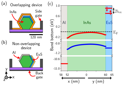
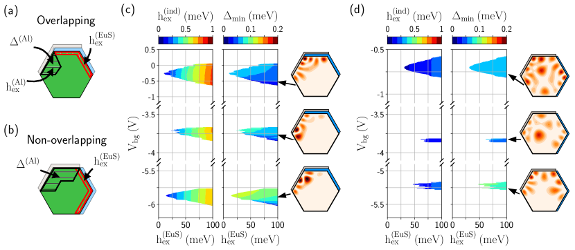
Device geometries and model.— Following closely the experiments of Ref. Vaitiekėnas et al., 2021, we consider the two types of device geometries depicted in Fig. 1(a) and (b). In both cases, a hexagonal cross-section InAs nanowire is partially covered by epitaxial Al and EuS layers. The main difference between them is that, in the overlapping device [Fig. 1(a)], the Al and EuS layers partially overlap on one facet, while in the non-overlapping one [Fig. 1(b)] they lie on adjacent facets. Various dielectrics surrounding the hybrid wires are included in our electrostatic simulations although we find that they play a minor role. Last, there are three gate electrodes used in the experiments to tune the electrostatic potential inside the devices: one back-gate and two side-gates. We analyze other geometries in the Supplemental Material (SM) Sup, .
In this work we address the bulk electronic properties of these hybrid nanowires, which we assume are translational invariant along the direction. A schematic band diagram of the three different materials in the transverse directions, , can be seen in Fig. 1(c). The Al layer is a metal whose conduction band lies at eV below the Fermi level Ashcroft and Mermin (1976). Despite the fact that the conduction band of the InAs is typically at the Fermi level, experimental angle-resolved photoemission spectroscopy (ARPES) Schuwalow et al. (2019) and scanning tunneling microscopy (STM) Reiner et al. (2020) measurements on epitaxial Al/InAs structures show that there is a band offset of eV between the Al and the InAs. This imposes an electron doping of the InAs conduction band close to the Al/InAs interface. On the other hand, soft x-ray ARPES (SX-ARPES) experiments on the EuS/InAs interface Liu et al. (2020a) indicate that the InAs conduction band lies well within the EuS band gap, which is of the order of eV Eastman et al. (1969). In particular, the EuS conduction band is located 0.7 eV above the Fermi level and the valence bands eV below Eastman et al. (1969); Liu et al. (2020a). The EuS conduction band is characterized by an exchange field that shifts the spin-up and spin-down energies by roughly meV Mauger and Godart (1986); Moodera et al. (2007); Alphenaar et al. (2009). In addition to this, and similarly to the InAs/Al interface, SX-ARPES experiments Liu et al. (2020a) also revealed a band bending of the order of eV at the InAs/EuS interface, which imposes a smaller charge accumulation at this junction as well. All these band alignments are further distorted by the electric fields defined by the gate electrodes. However, for sufficiently small fields one can assume that only the InAs conduction band moves and can neglect its hybridization with the EuS valence bands (see the SM Sup for further details).
Under these assumptions, we describe the wires using the following continuous model Hamiltonian
| (1) |
where , , and and denote Pauli matrices in spin and Nambu spaces, respectively. The parameters , , and , corresponding to the effective mass, Fermi energy, exchange field and superconducting pairing amplitude, are taken differently for each region according to estimations from the literature, as summarized in Table I of the SM Sup . To simulate the disordered outer surface of the Al layer and the irregular EuS/Al interface we introduce a random Gaussian noise in Sup . The other parameters, i.e., the electrostatic potential and the spin-orbit coupling (SOC) inside the wire , are determined in a self-consistent way. For this purpose, we obtain by solving the Schrödinger-Poisson equations within the Thomas-Fermi approximation Mikkelsen et al. (2018); Escribano et al. (2019). The SOC varies locally with the electric field and is accurately calculated using the procedure described in Ref. Escribano et al., 2020, see also Sup, . Notice that the exchange field does not give rise to a magnetic orbital term in the Hamiltonian, as opposed to what happens in wires under an external magnetic field Nijholt and Akhmerov (2016); Kiczek and Ptok (2017); Dmytruk and Klinovaja (2018); Winkler et al. (2019).
To obtain the electronic properties we diagonalize Eq. (1). To this end, we discretize it into a tight-binding Hamiltonian using an appropriate mesh, which is dictated by the Al Fermi wavelength Sup . Notice that a description of the three material regions (Al, InAs and EuS) on the same footing constitutes a demanding computational task. In the second part of this work we build a simplified model in which we integrate out the Al and EuS layers and include their proximity effects over the InAs wire as position-dependent effective parameters. This allows us to explore the system’s phase diagram for a broader range of parameters.
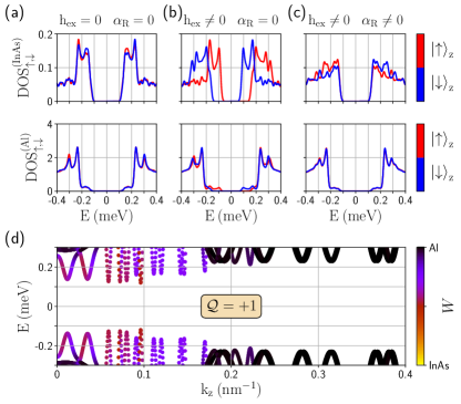
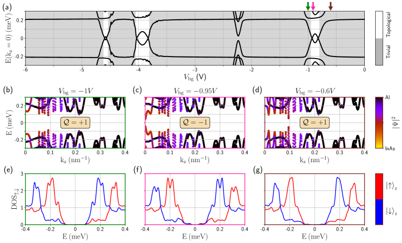
Full model results.— We first focus on the density of states (DOS) and dispersion relation of the overlapping geometry (see Fig. 2) fixing the side-gate voltages to zero and the back-gate to V. In order to identify the separate effect of the magnetic and superconducting terms, we perform three different calculations: in the first one we switch off the exchange field in the EuS and the Rashba SOC in the InAs [Fig. 2(a)]; then we switch on [Fig. 2(b)] and finally we also connect [Fig. 2(c)].
In the top panel of Fig. 2(a) we show the partial DOS integrated over the InAs volume. It exhibits a well-defined induced superconducting gap, although halved with respect to the meV gap observed in the DOS integrated over the Al shell volume, Fig. 2(a) bottom panel. This is in accordance with what one expects from a conventional superconducting proximity effect Chang et al. (2018); de Moor et al. (2018); Winkler et al. (2019).
When (but ) we observe two main features in the spin-resolved partial DOS. First, an energy splitting of the superconducting coherence peak appears in the Al [Fig. 2(b) bottom panel], which is of the order of meV, in agreement with recent theoretical and experimental results on Al/EuS junctions Hao et al. (1991); Strambini et al. (2017); Rouco et al. (2019); Zhang et al. (2020). This agreement without any fine tuning of the parameters in our model is encouraging about its validity. Second, there is a complete closing of the induced gap in the InAs [Fig. 2(b) top panel]. This points to an induced exchange field larger than meV, the induced gap in the semiconductor, and therefore, larger than in the Al layer. In contrast to previous proposals Liu et al. (2020b); Vaitiekėnas et al. (2021) our results suggest that in the current case topological superconductivity is achieved below the Chandrasekar-Clogston limit Chandrasekhar (1962); Clogston (1962) for the Al ().
Finally, in Fig. 2(c) top panel we observe that a gap is opened again in the presence of SOC. This sequence of gap closing and reopening at a high-symmetry -point is a signature of a topological phase transition. The band structure shown in Fig. 2(d) further illustrates the spatial distribution of the low-energy states in this last case (i.e., with and ). The weight of each state in the different materials is represented with colors, from a state completely located in the Al layer (black) to one completely located in the InAs wire (yellow). The lowest-energy states close to have significant weight both in the Al and in the InAs, as expected for a topological superconducting phase Winkler et al. (2019). We prove that the system in Figs. 2(c) and 2(d) is indeed in the topological regime by calculating the topological invariant . For large Hamiltonian matrices, this can be achieved by computing the Chern number from the eigenvalues of the Wilson matrix, which only involves the lowest-energy eigenstates at the Brillouin zone borders Sup . We find , which actually corresponds to the nontrivial case.
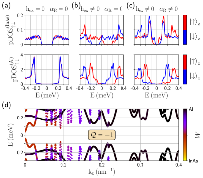
Strikingly, the same analysis for the non-overlapping geometry (Fig. 3) reveals that the magnetic proximity effect in this case is not strong enough to close and reopen the superconducting gap in the wire. The reason for this behavior can be traced to the limited spin polarization induced in the nanowire for this geometry. Hence, there is no topological phase in this case, at least for this choice of gate voltages.
Simplified model and phase diagram.— We consider now the Hamiltonian of Eq. (1) restricted to the InAs wire, where we include an effective pairing amplitude meV and an exchange field meV on the cross-section regions closer to the Al and the EuS shells, respectively, as schematically depicted in Figs. 4(a) and (b). We also include a smaller exchange coupling meV in the Al-proximitized region of the overlapping device. The magnitude of these parameters and the extension of the corresponding regions are extracted by adjusting to the behavior of the full model results, as shown in the SM Sup .
In Fig. 4(c) we present the topological phase diagram of the overlapping device as a function of the back-gate voltage and the exchange field of the EuS. Notice that should be meV according to our full model. However, departures from the idealized model of Eq. (1) might reduce the value of the induced magnetic exchange. For instance, the mismatch between the minima of the InAs conduction band (at the point) and the EuS one (at the point Nirpendra et al. (2007)) could suppress their hybridization depending on material growth directions or other details (see the SM Sup ), leading to a smaller value. Thus we allow this parameter to vary between and meV to evaluate the robustness of our results with respect to this value. With colors, in the left panel of Fig. 4(c) we show the induced exchange coupling, 111Note that the induced exchange coupling in the wire, , is much smaller (approximately one per cent Sup ) than the EuS parent Zeeman field, ., and in the middle panel the induced minigap, , for the energy state closest to the Fermi energy in both cases. In these plots, white means trivial (i.e., ), while the colored regions correspond to the topological phase. There are several topological regions against corresponding to different transverse subbands. In those regions, the condition that is larger than the square root of the induced gap squared plus the chemical potential squared is fulfilled, as expected Lutchyn et al. (2010); Oreg et al. (2010). To the right in Fig. 4(c) we show the probability density of the transverse subband closer to the Fermi level at across the wire section for the parameters indicated with arrows. In the three cases exhibited, the wavefunction concentrates both around the left-upper facet covered by Al, and the top facet where the Al and EuS layers overlap. This is consistent with the requirement of maximizing simultaneously the superconducting and magnetic proximity effects.
The phase diagram for the non-overlapping device is shown in Fig. 4(d). The extension of the topological phase is very much reduced, almost negligible for some subbands. It is interesting to observe that, for realistic gate potential values, the wavefunction needs to be very spread across the wire section in order to acquire the superconducting and magnetic correlations for the topological phase to develop. This in turn translates into narrow back-gate voltage ranges for which this is possible and small topological minigaps.
In the SM Sup we further analyze the previous phase diagrams as a function of the right-side gate voltage, obtaining similar results. We also consider alternative geometries, nevertheless finding that the overlapping configuration of Fig. 1(a) gives rise to more extended, robust and tunable topological regions for realistic parameters. In particular, we find that the best way to optimize the topological state (i.e., increase its minigap) is by fixing a large negative back-gate potential and a small positive right-side gate potential. In doing so, the wavefunction is pushed towards the superconductor-ferromagnet corner of the wire and thus the superconducting and magnetic proximity effects are maximized.
Conclusions.— From calculations of the DOS, band structure, topological invariant and the phase diagram, we conclude that the hybrid InAs/Al/EuS nanowires studied in Ref. Vaitiekėnas et al., 2021 can exhibit topological superconductivity under certain geometrical and gating conditions. For a topological phase to exist, the nanowire wavefunction must acquire both superconducting and magnetic correlations such that the induced exchange field exceeds the induced pairing. Since the proximity effects occur only in wire cross-section regions close to the Al and EuS layers, the wavefunction needs to be pushed simultaneously close to both materials by means of nearby gates. Our numerical simulations demonstrate that this is electrostatically favorable in device geometries where the Al and EuS shells overlap over some wire facet. This configuration is further advantageous in that, apart from a direct magnetization from the EuS layer in contact to the wire, there is an indirect one through the Al layer, which favors reaching the topological condition. While our model includes the effect of disorder at the Al layer surface and at the EuS/Al interface, we have not considered other sources of disorder, like ,e.g., the presence of magnetic domains. However, these domains can be aligned by the application of a small field that is then switched to zero, as done in Ref. Vaitiekėnas et al. (2021). A subsequent study which considers a fully diffusive Al layer Khindanov et al. (2021) reaches similar conclusions as our work (although disorder increases the induced exchange field required to achieve a topological phase).
Finally, as a side outcome, our microscopic analysis demonstrates the tunability of the magnetic and superconducting induced couplings in the nanowire. This opens up the possibility of engineering the material geometries, their disposition, and the electrostatic environment to enter and abandon the topological regime at will and, thus, the appearance of Majorana modes. These ideas can be applied to other materials and experimental arrangements, which surely will favor more experiments in the field, as well as in other fields such as superconducting spintronics.
Acknowledgments.— We would like to thank S. Vaitiekėnas and C. M. Marcus for illuminating discussions on their experimental results. We also thank M. Alvarado and O. Lesser for valuable help with the topological invariant calculation. A.L.Y. and E.P. acknowledge support from the Spanish MICINN through Grants No. FIS2016-80434-P (AEI/FEDER, EU) and No. FIS2017-84860-R, by EU through Grant No. 828948 (AndQC), and through the “María de Maeztu” Programme for Units of Excellence in R&D (Grant No. MDM-2014-0377). Y.O. acknowledges partial support through the ERC under the European Union’s Horizon 2020 research and innovation programme (Grant Agreement LEGOTOP No. 788715), the ISF Quantum Science and Technology (2074/19), the BSF and NSF (2018643), and the CRC/Transregio 183.
References
- Aguado (2017) R. Aguado, La Rivista del Nuovo Cimento 40, 523 (2017).
- Lutchyn et al. (2018) R. M. Lutchyn, E. P. A. M. Bakkers, L. P. Kouwenhoven, P. Krogstrup, C. M. Marcus, and Y. Oreg, Nature Reviews Materials 3, 2058 (2018).
- Prada et al. (2020) E. Prada, P. San-Jose, M. W. A. de Moor, A. Geresdi, E. J. H. Lee, J. Klinovaja, D. Loss, J. Nygård, R. Aguado, and L. P. Kouwenhoven, Nature Reviews Physics 2, 575 (2020).
- Lutchyn et al. (2010) R. M. Lutchyn, J. D. Sau, and S. Das Sarma, Phys. Rev. Lett. 105, 077001 (2010).
- Oreg et al. (2010) Y. Oreg, G. Refael, and F. von Oppen, Phys. Rev. Lett. 105, 177002 (2010).
- Plugge et al. (2017) S. Plugge, A. Rasmussen, R. Egger, and K. Flensberg, New Journal of Physics 19, 012001 (2017).
- Karzig et al. (2017) T. Karzig, C. Knapp, R. M. Lutchyn, P. Bonderson, M. B. Hastings, C. Nayak, J. Alicea, K. Flensberg, S. Plugge, Y. Oreg, C. M. Marcus, and M. H. Freedman, Phys. Rev. B 95, 235305 (2017).
- Vaitiekėnas et al. (2021) S. Vaitiekėnas, Y. Liu, C. M. Marcus, and P. Krogstrup, Nature Physics 17, 43 (2021).
- Liu et al. (2020a) Y. Liu, A. Luchini, S. Martí-Sánchez, C. Koch, S. Schuwalow, S. A. Khan, T. Stankevič, S. Francoual, J. R. L. Mardegan, J. A. Krieger, V. N. Strocov, J. Stahn, C. A. F. Vaz, M. Ramakrishnan, U. Staub, K. Lefmann, G. Aeppli, J. Arbiol, and P. Krogstrup, ACS Applied Materials & Interfaces 12, 8780 (2020a).
- Liu et al. (2020b) Y. Liu, S. Vaitiekėnas, S. Martí-Sánchez, C. Koch, S. Hart, Z. Cui, T. Kanne, S. A. Khan, R. Tanta, S. Upadhyay, M. E. n. Cachaza, C. M. Marcus, J. Arbiol, K. A. Moler, and P. Krogstrup, Nano Letters 20, 456 (2020b).
- Sau et al. (2010) J. D. Sau, R. M. Lutchyn, S. Tewari, and S. Das Sarma, Phys. Rev. Lett. 104, 040502 (2010).
- Wolf et al. (2001) S. A. Wolf, D. D. Awschalom, R. A. Buhrman, J. M. Daughton, S. von Molnár, M. L. Roukes, A. Y. Chtchelkanova, and D. M. Treger, Science 294, 1488 (2001).
- Linder and Robinson (2015) J. Linder and J. W. A. Robinson, Nature Physics 11, 1745 (2015).
- Giazotto et al. (2006) F. Giazotto, T. T. Heikkilä, A. Luukanen, A. M. Savin, and J. P. Pekola, Rev. Mod. Phys. 78, 217 (2006).
- Machon et al. (2013) P. Machon, M. Eschrig, and W. Belzig, Phys. Rev. Lett. 110, 047002 (2013).
- Woods and Stanescu (2020) B. D. Woods and T. D. Stanescu, “Electrostatic effects and topological superconductivity in semiconductor-superconductor-magnetic insulator hybrid wires,” (2020), arXiv:2011.01933 [cond-mat.mes-hall] .
- Maiani et al. (2021) A. Maiani, R. Seoane Souto, M. Leijnse, and K. Flensberg, Phys. Rev. B 103, 104508 (2021).
- Liu et al. (2020c) C.-X. Liu, S. Schuwalow, Y. Liu, K. Vilkelis, A. L. R. Manesco, P. Krogstrup, and M. Wimmer, “Electronic properties of inas/eus/al hybrid nanowires,” (2020c), arXiv:2011.06567 [cond-mat.mes-hall] .
- Langbehn et al. (2021) J. Langbehn, S. Acero González, P. W. Brouwer, and F. von Oppen, Phys. Rev. B 103, 165301 (2021).
- (20) See Supplemental Material at [url] for further details on the parameters and numerical methods used for our simulations, for an additional study of the phase diagram versus the side-gate potential, and for an analysis of a different geometry. The Supplemental Material includes Refs. Vurgaftman et al., 2001; Levinshtein et al., 2000; Thelander et al., 2010; Segall, 1961; Chiang and Dzyuba, 2017; Xavier, 1967; Axe, 1969; Robertson, 2004; Escribano, 2020; Altland and Zirnbauer, 1997; Schnyder et al., 2008; Loring and Hastings, 2010; Zhang et al., 2013; Lesser and Oreg, 2020; Yu et al., 2011; Alexandradinata et al., 2016; Bradlyn et al., 2019; Antipov et al., 2018; Escribano et al., 2018; Woods et al., 2020; Logg and Wells, 2010; Logg et al., 2012; Campos et al., 2018; Winkler et al., 2003; Gmitra and Fabian, 2016; Faria Junior et al., 2016 .
- Ashcroft and Mermin (1976) N. W. Ashcroft and N. D. Mermin, Solid State Physics, Vol. 1 (Saunders College Publishing, Philadelphia, 1976).
- Schuwalow et al. (2019) S. Schuwalow, N. B. M. Schroeter, J. Gukelberger, C. Thomas, V. Strocov, J. Gamble, A. Chikina, M. Caputo, J. Krieger, G. C. Gardner, M. Troyer, G. Aeppli, M. J. Manfra, and P. Krogstrup, “Band bending profile and band offset extraction at semiconductor-metal interfaces,” (2019), arXiv:1910.02735 [cond-mat.mtrl-sci] .
- Reiner et al. (2020) J. Reiner, A. K. Nayak, A. Tulchinsky, A. Steinbok, T. Koren, N. Morali, R. Batabyal, J.-H. Kang, N. Avraham, Y. Oreg, H. Shtrikman, and H. Beidenkopf, Phys. Rev. X 10, 011002 (2020).
- Eastman et al. (1969) D. E. Eastman, F. Holtzberg, and S. Methfessel, Phys. Rev. Lett. 23, 226 (1969).
- Mauger and Godart (1986) A. Mauger and C. Godart, Physics Reports 141, 51 (1986).
- Moodera et al. (2007) J. S. Moodera, T. S. Santos, and T. Nagahama, Journal of Physics: Condensed Matter 19, 165202 (2007).
- Alphenaar et al. (2009) B. W. Alphenaar, A. D. Mohite, J. S. Moodera, and T. S. Santos, in Physical Chemistry of Interfaces and Nanomaterials VIII, Vol. 7396, edited by O. L. A. Monti and O. V. Prezhdo, International Society for Optics and Photonics (SPIE, 2009) pp. 24 – 32.
- Mikkelsen et al. (2018) A. E. G. Mikkelsen, P. Kotetes, P. Krogstrup, and K. Flensberg, Phys. Rev. X 8, 031040 (2018).
- Escribano et al. (2019) S. D. Escribano, A. Levy Yeyati, Y. Oreg, and E. Prada, Phys. Rev. B 100, 045301 (2019).
- Escribano et al. (2020) S. D. Escribano, A. L. Yeyati, and E. Prada, Phys. Rev. Research 2, 033264 (2020).
- Nijholt and Akhmerov (2016) B. Nijholt and A. R. Akhmerov, Phys. Rev. B 93, 235434 (2016).
- Kiczek and Ptok (2017) B. Kiczek and A. Ptok, Journal of Physics: Condensed Matter 29, 495301 (2017).
- Dmytruk and Klinovaja (2018) O. Dmytruk and J. Klinovaja, Phys. Rev. B 97, 155409 (2018).
- Winkler et al. (2019) G. W. Winkler, A. E. Antipov, B. van Heck, A. A. Soluyanov, L. I. Glazman, M. Wimmer, and R. M. Lutchyn, Phys. Rev. B 99, 245408 (2019).
- Chang et al. (2018) W. Chang, S. M. Albrecht, T. S. Jespersen, F. Kuemmeth, P. Krogstrup, J. Nygård, and C. M. Marcus, Nature Nanotechnology 10, 232 (2018).
- de Moor et al. (2018) M. W. A. de Moor, J. D. S. Bommer, D. Xu, G. W. Winkler, A. E. Antipov, A. Bargerbos, G. Wang, N. van Loo, R. L. M. O. h. Veld, S. Gazibegovic, D. Car, J. A. Logan, M. Pendharkar, J. S. Lee, E. P. A. M. Bakkers, C. J. Palmstrøm, R. M. Lutchyn, L. P. Kouwenhoven, and H. Zhang, New Journal of Physics 20, 103049 (2018).
- Hao et al. (1991) X. Hao, J. S. Moodera, and R. Meservey, Phys. Rev. Lett. 67, 1342 (1991).
- Strambini et al. (2017) E. Strambini, V. N. Golovach, G. De Simoni, J. S. Moodera, F. S. Bergeret, and F. Giazotto, Phys. Rev. Materials 1, 054402 (2017).
- Rouco et al. (2019) M. Rouco, S. Chakraborty, F. Aikebaier, V. N. Golovach, E. Strambini, J. S. Moodera, F. Giazotto, T. T. Heikkilä, and F. S. Bergeret, Phys. Rev. B 100, 184501 (2019).
- Zhang et al. (2020) X. P. Zhang, V. N. Golovach, F. Giazotto, and F. S. Bergeret, Phys. Rev. B 101, 180502 (2020).
- Chandrasekhar (1962) B. S. Chandrasekhar, Applied Physics Letters 1, 7 (1962).
- Clogston (1962) A. M. Clogston, Phys. Rev. Lett. 9, 266 (1962).
- Nirpendra et al. (2007) S. Nirpendra, M. Sapan, N. Tashi, and A. Sushil, Physica B: Condensed Matter 388, 99 (2007).
- Note (1) Note that the induced exchange coupling in the wire, , is much smaller (approximately one per cent Sup ) than the EuS parent Zeeman field, .
- Khindanov et al. (2021) A. Khindanov, J. Alicea, P. Lee, W. S. Cole, and A. E. Antipov, Phys. Rev. B 103, 134506 (2021).
- Vurgaftman et al. (2001) I. Vurgaftman, J. R. Meyer, and L. R. Ram-Mohan, Journal of Applied Physics 89, 5815 (2001).
- Levinshtein et al. (2000) M. Levinshtein, S. Rumyantsev, and M. Shur, Handbook series on semiconductor parameters, Vol. 1 (World Scientific Publishing, 2000).
- Thelander et al. (2010) C. Thelander, K. A. Dick, M. T. Borgström, L. E. Fröberg, P. Caroff, H. A. Nilsson, and L. Samuelson, Nanotechnology 21, 205703 (2010).
- Segall (1961) B. Segall, Phys. Rev. 124, 1797 (1961).
- Chiang and Dzyuba (2017) Y. N. Chiang and M. O. Dzyuba, EPL (Europhysics Letters) 120, 17001 (2017).
- Xavier (1967) R. M. Xavier, Physics Letters A 25, 244 (1967).
- Axe (1969) J. Axe, Journal of Physics and Chemistry of Solids 30, 1403 (1969).
- Robertson (2004) J. Robertson, Eur. Phys. J. Appl. Phys. 28, 265 (2004).
- Escribano (2020) S. D. Escribano, “MajoranaNanowires Quantum Simulation Package,” (2020).
- Altland and Zirnbauer (1997) A. Altland and M. R. Zirnbauer, Phys. Rev. B 55, 1142 (1997).
- Schnyder et al. (2008) A. P. Schnyder, S. Ryu, A. Furusaki, and A. W. W. Ludwig, Phys. Rev. B 78, 195125 (2008).
- Loring and Hastings (2010) T. A. Loring and M. B. Hastings, EPL (Europhysics Letters) 92, 67004 (2010).
- Zhang et al. (2013) Y.-F. Zhang, Y.-Y. Yang, Y. Ju, L. Sheng, R. Shen, D.-N. Sheng, and D.-Y. Xing, Chinese Physics B 22, 117312 (2013).
- Lesser and Oreg (2020) O. Lesser and Y. Oreg, Phys. Rev. Research 2, 023063 (2020).
- Yu et al. (2011) R. Yu, X. L. Qi, A. Bernevig, Z. Fang, and X. Dai, Phys. Rev. B 84, 075119 (2011).
- Alexandradinata et al. (2016) A. Alexandradinata, Z. Wang, and B. A. Bernevig, Phys. Rev. X 6, 021008 (2016).
- Bradlyn et al. (2019) B. Bradlyn, Z. Wang, J. Cano, and B. A. Bernevig, Phys. Rev. B 99, 045140 (2019).
- Antipov et al. (2018) A. E. Antipov, A. Bargerbos, G. W. Winkler, B. Bauer, E. Rossi, and R. M. Lutchyn, Phys. Rev. X 8, 031041 (2018).
- Escribano et al. (2018) S. D. Escribano, A. L. Yeyati, and E. Prada, Beilstein Journal of Nanotechnology 9, 2171 (2018).
- Woods et al. (2020) B. D. Woods, S. Das Sarma, and T. D. Stanescu, Phys. Rev. B 101, 045405 (2020).
- Logg and Wells (2010) A. Logg and G. N. Wells, ACM Transactions on Mathematical Software 37, 1 (2010).
- Logg et al. (2012) A. Logg, K.-A. Mardal, G. N. Wells, et al., Automated Solution of Differential Equations by the Finite Element Method (Springer, Berlin, Heidelberg, 2012).
- Campos et al. (2018) T. Campos, P. E. Faria Junior, M. Gmitra, G. M. Sipahi, and J. Fabian, Phys. Rev. B 97, 245402 (2018).
- Winkler et al. (2003) R. Winkler, S. Papadakis, E. De Poortere, and M. Shayegan, Spin-Orbit Coupling in Two-Dimensional Electron and Hole Systems, Vol. 41 (Springer, Berlin, Heidelberg, 2003).
- Gmitra and Fabian (2016) M. Gmitra and J. Fabian, Phys. Rev. B 94, 165202 (2016).
- Faria Junior et al. (2016) P. E. Faria Junior, T. Campos, C. M. O. Bastos, M. Gmitra, J. Fabian, and G. M. Sipahi, Phys. Rev. B 93, 235204 (2016).
- Note (2) We ignore the contribution coming from the valence bands as they could only play a role for V in our simulations.
- Note (3) Note that, because right and left side gates are placed parallel to each other and symmetric with respect to the wire, they provide comparable phase diagrams.
Supplemental Material
Numerical implementation
In this section we describe the specific details of the two geometries (overlapping and non-overlapping) considered in the main text, as well as their characteristic material parameters. In addition, we explain how we perform the numerical calculations for their electronic structure including the effect of the electrostatic potential.
1. Geometry
A sketch of the two devices analyzed in this work is shown in Fig. 1 of the main text. In both cases a hexagonal cross-section InAs nanowire (in green) of radius nm is partially covered by two different thin layers. Both are grown epitaxially over certain facets of the wire. The highly transparent epitaxial interfaces improve the hybridization between the nanowire and the layers. One of these layers is a 6 nm-thick shell made of superconducting Al (light grey), whose outer surface (2 nm-thick) is oxidized. The other layer is made of EuS (blue), a well-known ferromagnetic insulator, and its width is 8 nm in the overlapping device and 5 nm in the non-overlapping one. Despite the difference between these two values, we find that the precise thickness of the EuS, for the ferromagnetic exchange coupling mechanism studied here, plays a negligible role because it acts as a mere (magnetic) insulator. We note that, in the overlapping device, the interface between the Al and the EuS is also grown epitaxially in the experiments but the interface is not completely flat. This roughness is characterized by a corrugation width of nm.
This hybrid system is surrounded by three gates (dark grey), one at the bottom and two at the left and right sides, which allow to tune the wire doping level and the charge distribution inside the heterostructure simultaneously. The side gates are placed symmetrically from the center of the wire at nm distance from the outer corners of the wire, and their height is half the wire’s width. On the other hand, the wire is placed on top of a SiO2 dielectric substrate (violet) with a thickness of nm. This substrate fixes the distance between the back gate and the bottom of the wire.
There are other dielectrics in the devices that are necessary to avoid the unwanted oxidation of the EuS layer. They are a 8 nm-thick layer of HfO2 (orange) surrounding the whole heterostructure in the overlpaping device, and a nm-thick layer of AlO2 (yellow) covering the EuS layer in the non-overlapping one. We include them in our electrostatic simulations to obtain a better qualitative agreement with the experiment of Ref. Vaitiekėnas et al., 2021 although they play a minor role in our results. Finally, we assume that the rest of the environment (white) is vacuum. We summarize all these geometrical parameters in Table 1.
| Material | Parameter | Value | Refs. |
| InAs | width | 120 nm | - |
| height | 104 nm | ||
| 0.023 | Vurgaftman et al.,2001 | ||
| 0 | Liu et al.,2020a | ||
| 0 | - | ||
| 0 | - | ||
| (see text for details) | |||
| 15.5 | Levinshtein et al.,2000 | ||
| Thelander et al., 2010, Reiner et al.,2020 | |||
| Al | width | 6 nm | - |
| oxidation width | 2 nm | ||
| Segall,1961 | |||
| -11.7 eV | Ashcroft and Mermin,1976 | ||
| 0 | - | ||
| 0.23 meV | Chang et al.,2018 | ||
| 0 | Chiang and Dzyuba,2017 | ||
| - | |||
| 0.2 eV | Reiner et al., 2020, Schuwalow et al., 2019, Liu et al.,2020c | ||
| EuS | width222Note that in the experiments, the width of the EuS layer is nm in the overlapping device while it is nm in the non-overlapping one. | 8/5 nm | - |
| corrugation width | 1nm | Liu et al.,2020b | |
| 0.3 | Xavier,1967 | ||
| 0.8 eV | Alphenaar et al., 2009, Liu et al.,2020a | ||
| 0.1 eV | Mauger and Godart, 1986, Alphenaar et al.,2009 | ||
| 0 | - | ||
| 333We have found no explicit information about the SO coupling in EuS materials. We therefore assume that it is negligibly small. | 0 | - | |
| 10 | Axe,1969 | ||
| Dielectrics | SiO2 width | 200 nm | - |
| HfO2 width | 80 nm | ||
| Al2O3 width | 8 nm | ||
| 3.9 | Robertson,2004 | ||
| 25 | Levinshtein et al.,2000 | ||
| 10 | Levinshtein et al.,2000 | ||
| - | |||
2. Model Hamiltonian
The basic arguments leading to our continuum model Hamiltonian have been presented in the main text. As explained there, we focus on the InAs, Al and EuS conduction bands and neglect the InAs and EuS valence bands. Notice that the EuS conduction band has its minimum at the -point Nirpendra et al. (2007) rather than at , as InAs and Al do. When electrons tunnel from one material to the other, for instance from InAs to EuS, this could lead to momentum mismatch depending on the growth direction between both materials and thus to a decreased coupling. Moreover, the EuS could exhibit grains (or other forms of disorder), details which are beyond the qualitative analysis in this work. For this reason, we consider an effective continuum model for the different materials where the EuS conduction band minimum is also taken at the -point. We note that other sources of momentum mismatch coming from different effective masses, finite size materials, certain sources of disorder explained below, etc., are taken into account. This model, which we call full model in the main text, gives an optimistic hybridization between EuS and InAs. Since the boundary between the EuS and Al is disordered (see below), our model essentially describes correctly this hybridization as momentum conservation along that interface breaks under such disorder.
Under the assumptions presented above, we arrive to the following Bogoliubov-de Gennes Hamiltonian to describe the heterostructure (Eq. (1) in the main text)
| (2) | |||||
where is the momentum operator vector, is the radial spatial operator vector (for a translational-invariant wire along ), and and are the Pauli matrices in spin and Nambu space, respectively. The first term in Eq. (2) is the kinetic energy, where is the effective mass that takes different constant values inside the different parts of the heterostructure. The function is the spatial-dependent electrostatic potential across the section of the hybrid nanowire. In the following subsection we explain in detail how we compute it. The quantity is the energy difference at between the band bottom of the conduction band (in each region) and the Fermi level of the entire heterostructure, which we fix to zero in this work. To simulate the disordered outer surface of the Al (the oxidized region) and the irregular EuS/Al interface, we assume that in these disordered regions is characterized by a random Gaussian noise with a standard deviation of 10% of the Fermi energy in the material. This accidental disorder breaks the parallel momentum conservation leading to an enhanced hybridization between the wire’s and the layers’ electronic states Winkler et al. (2019). The operators and are the exchange field and the superconducting pairing amplitude, which take non-zero values only in the EuS and Al layers, respectively. Finally, the last term in Eq. (2) is the spin-orbit (SO) interaction, where is the so-called SO coupling. In the last subsection we discuss separately how we describe it for the whole heterostructure. The different values for the parameters that we use in our simulations, together with the references from where they are extracted, are shown in Table 1.
We perform a numerical diagonalization of the Hamiltonian (2) to obtain the eigenspectrum. To this end, we discretize this continuum model into a tight-binding Hamiltonian. We perform the discretization only in the and directions (the section of the wire), and we assume that in the other direction (the wire’s direction ) the nanowire is translationally invariant. In the directions and the momentum must be substituted by their corresponding partial derivatives, i.e., and , and then the partial derivatives can be discretized using the central difference method, e.g.
| (3) |
where is the mesh spacing. We choose such that the grid can accommodate the Fermi wavelength of the eigenstates. Otherwise, a poor spacing would lead to spurious solutions. As Al is a metal with a large Fermi energy, it is characterized by a large Fermi momentum, which implies that a small mesh spacing must be used. We find that nm is a reasonable mesh size in our simulations. Once the Hamiltonian is transformed into a tight-binding one, we diagonalize it numerically (for each and values) using the standard ARPACK tools provided by the package Scipy of Python. This gives as a result the energy subbands for the different transverse subbands index , and their corresponding wavefunctions , which are actually four-component spinors. We perform this diagonalization using the Python package MajoranaNanowires Escribano (2020).
As the three materials that comprise the hybrid wire are coupled, the energy subbands correspond to wavefunctions that spread all across the heterostructure. To characterize the weight of the wavefunction on a certain material , we project the probability density of any state onto this region,
| (4) |
In close relation to this quantity, we also compute the spin-polarized partial density of states (pDOS), i.e., the DOS integrated over different regions , using the following expression
| (5) |
If includes the three materials in this equation, then the resulting expression is the total spin-polarized in the device. Then, one can compute the total DOS by summing both spin directions, .
Lastly, to characterize the -class topological phase Altland and Zirnbauer (1997); Schnyder et al. (2008) (to which the Majorana nanowires belong), we compute the Chern number
| (6) |
where denotes the first Brillouin zone ( in our system), and is the ground state of the system, i.e., the Slater determinant of all the -th eigenstates whose energies are below the Fermi energy. To easily compute numerically the Chern number we perform some transformations following the ideas of Refs. Loring and Hastings, 2010; Zhang et al., 2013; Lesser and Oreg, 2020. First, we apply the Stokes theorem
| (7) |
in such a way that the (line) integral is now performed through a closed contour around the reciprocal unit cell. Then, we discretize the momentum space , what allows us to replace the derivatives by finite differences and the integral by a summation over the reciprocal space points
| (8) |
where is the complex argument function of a complex number . The product of Slater determinants in the above equation can be rewritten as a determinant of a matrix , whose matrix element can be directly written in terms of the eigenfunctions of the Hamiltonian,
| (9) |
From this, the Chern number is simply given by
| (10) |
where is the so-called Wilson matrix in the literature Yu et al. (2011); Alexandradinata et al. (2016); Bradlyn et al. (2019). Finally, we use that the determinant of any square matrix can be written as the product of its eigenvalues to rewrite the expression as
| (11) |
where are all the eigenvalues of the Wilson matrix . In practice, it is enough to include only the high-symmetry -points in the product inside the Wilson matrix. In our case, these points are , which gives as a result the Wilson matrix
| (12) |
Additionally, notice that in principle the matrix involves all the eigenstates of the Hamiltonian (below the Fermi level) at two different points, and , as shown in Eq. (9). But since only the non-trivial topological eigenstates provide a non-zero contribution to the Chern number, and these states can only emerge close to the Fermi level in the studied system, it is therefore enough to include the closest states to the Fermi level in the Wilson matrix. This assumption allows to significantly alleviate the computational effort in our calculations.
To summarize this last part, the procedure that we follow in order to compute the topological invariant is the following: We first calculate the eigenstates of the Hamiltonian at . We need only those -th states that are below and close to the Fermi energy. We find that eigenstates are enough in our system to properly characterize the topological phase. We then compute the coupling matrices of Eq. (9) and, from them, the Wilson matrix using Eq. (12). We calculate its eigenvalues , and from them we compute the Chern number using Eq. (11), which is a positive integer. We finally identify the topological invariant
| (13) |
which is positive (+1) for the trivial topological phase and negative (-1) for the non-trivial one.
3. Electrostatic potential
We obtain the electrostatic potential by solving the Poisson equation across the section of the wire,
| (14) |
where is the dielectric permitivity, and is the charge inside the heterostructure. On the one hand, is characterized by a different constant value inside each material (see Table 1), leading to abrupt jumps at the interfaces. Note that the Poisson equation must be solved on the entire system, including the dielectric environment. On the other hand, the charge inside the hybrid nanowire is given by,
| (15) |
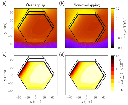
The term models the surface charge that is typically present in the uncovered nanowire facets Thelander et al. (2010); Reiner et al. (2020). We model it as a positive charge-density layer of thickness 1 nm in every nanowire facet not covered by the Al Winkler et al. (2019); Escribano et al. (2020). This leads to a band bending at these facets and, thus, to an accumulation of charge in the wire in those regions [see Fig. 1(c)]. In principle, the wire facets covered by EuS should not display this type of charge accumulation layer because the EuS is grown epitaxially. However, recent experiments Liu et al. (2020a) showed that there is a band bending at the EuS/InAs interface of the same magnitude as the one between InAs and air. Hence, we model both phenomena with the same . We find that creates a band bending of 0.1 eV, which is the value reported in experiments for InAs/vacuum Thelander et al. (2010); Reiner et al. (2020) and InAs/EuS Liu et al. (2020a) interfaces.
The second term in Eq. (15) corresponds to the mobile charges inside the hybrid structure. In principle, they should be computed from the solutions of the Schrödinger equation using the Hamiltonian of Eq. (2). Since this equation depends in turn on the electrostatic potential given by the Poisson equation of Eq. (14), the Schrödinger-Poisson equations have to be solved together in a self-consistent way. To reduce the computational effort, we use the Thomas-Fermi approximation. Within this approximation, one assumes that the charge density of the wire is given by the one of a non-interacting 3D electron-gas 444We ignore the contribution coming from the valence bands as they could only play a role for V in our simulations.
| (16) |
where is the Fermi-Dirac distribution for a given energy and temperature . This approximation has been used in previous works Mikkelsen et al. (2018); Escribano et al. (2019, 2020) on InAs nanowires and Al/InAs heterostructures, where it is demonstrated that it provides an excellent agreement with the results of the full Schrödinger-Poisson calculations. In this way, both equations are decoupled and, therefore, one only needs to diagonalize the Hamiltonian once for each potential (and momentum ).
Nonetheless, the Poisson equation still needs to be solved self-consistently [note that depends on ], although at a reduced computational cost. To carry out this self-consistency we use an Anderson iterative mixing,
| (17) |
where is a certain iteration in the self-consistent process, and is the so-called Anderson coefficient which is a constant in the range . In the first step () we take and we compute the electrostatic potential using the Poisson equation. Then, at any other arbitrary step , we compute the charge density using Eq. (16) with the electrostatic potential found using the of the previous iteration . We finally find the charge density at the step (i.e., ) using the Anderson mixing between these two charge densities shown in the above equation. This mixing between two different steps ensures the convergence to the solution. We keep this iterative procedure until the cumulative error between and is below . To facilitate an efficient convergence, we choose as Anderson coefficient a self-adaptive one given by,
| (18) |
where is the maximum value that we allow the Anderson coefficient to take in order to ensure converge. We set this value to 0.1 in all our simulations.
To solve the Poisson equation, we also need to impose boundary conditions. We fix different potentials at the boundaries of the gates for the different simulations performed in this work. In addition to this, we fix a constant potential of eV at the boundaries with the Al shell. The electrostatic potential resulting from this last condition will create a band bending of the same magnitude at the InAs/Al interface [see Fig. 1(c)]. This band bending, reported in experiments Reiner et al. (2020); Schuwalow et al. (2019); Liu et al. (2020c), has been previously described in other theoretical works Mikkelsen et al. (2018); Antipov et al. (2018); Escribano et al. (2018); Winkler et al. (2019); Escribano et al. (2019); Woods et al. (2020) on similar InAs/Al heterostructures.
To solve the Poisson equation with the above ingredients we use Fenics Logg and Wells (2010); Logg et al. (2012), a finite element solver for Python. We use a mesh discretization of nm.
As we show in the main text, the precise geometries of the devices, the position of the Al and EuS shells on the InAs facets and the gates, play a key role in the appearance of a topological phase. To better illustrate this fact, we show in Fig. 5 the electrostatic potential in the overlapping (a) and the non-overlapping (b) devices. In these simulations, the back-gate voltage is set to a negative value, particularly V. This is a typical situation in our simulations and in the experiments, as one needs to deplete the wire in order to populate it with just a few bands. Hence, the electrostatic potential is negative at the bottom of the wire, while it is positive and maximum close to the Al/InAs interface due to the Al/InAs band bending. This is translated into an accumulation of (mobile) charges in this interface, quantity that we show in Fig. 5(c) and (d) for the same devices. Despite the similarity between the electrostatic profiles of both devices, we show in the main text that they give rise to a very different energy spectrum. This can be understood by noticing the position of the the charge density with respect to the EuS. The better part of the charge density is located at the Al/InAs interface. In the overlapping device [Fig. 5(c)], this charge is thus also close to the left part of the EuS layer (the top facet). On the contrary, the EuS layer in the non-overlapping device [Fig. 5(d)] is far apart from the charge density. This apparently minor difference is what enhances the hybridization with the EuS in the overlapping device, and what suppresses the same hybridization in the non-overlapping one. We remark that this hybridization is necessary to induce a strong enough exchange field in the wire, and therefore, to create a topological phase.
4. Spin-orbit coupling
The SO interaction included in the Hamiltonian of Eq. (2) arises whenever an spatial symmetry is broken. In this Hamiltonian, only linear terms with are included as they are known to be the dominant ones. The strength of the SO interaction is given by the SO coupling and its value depends on the precise material. For Al, the SO coupling is negligible Chiang and Dzyuba (2017), while for the EuS we have found no information about its value in the literature. We thus set to zero the SO coupling of both materials in our simulations. By contrast, the SO coupling in InAs nanowires can take large values Campos et al. (2018); Escribano et al. (2020). Because the topological protection of the Majorana nanowires depends strongly on the precise value of this interaction, a proper description is crucial to reach a good qualitative agreement with the experiments.
The SO coupling has, in general, two components Winkler et al. (2003),
| (19) |
where is the Dresselhaus term and the Rashba one. The Dresselhaus SO coupling arises when the crystal unit cell itself is not symmetric, leading to a bulk inversion asymmetry. Hence, it is a spatial independent value that only depends on the material and its precise crystallographic structure. For InAs nanowires, it is known to be negligible in (111) zinc-blende crystals, while its value is roughly (meVnm) in (0001) wurtzite ones Gmitra and Fabian (2016); Faria Junior et al. (2016). On the other hand, the Rashba SO coupling emerges when the mesoscopic system is not symmetric in some direction, as it happens when there are interfaces or potential gates. It can be accurately described for III-V compound semiconductors using the following equation
| (20) |
where is a parameter that depends on the material and its crystallographic structure, and and are the valence band and split-off bands, respectively. We show in Table 2 their values. This equation has been derived in a previous work Escribano et al. (2020), finding that it provides excellent results in comparison to both more sophisticated theories and experimental measurements.
| Crystal | Parameter | Value |
|---|---|---|
| (111) Zinc-blende | (0,0,0) | |
| 1300 meVnm | ||
| 417 meV | ||
| 390 meV | ||
| (0001) Wurtzite | (0,0,30) meVnm | |
| 700 meVnm | ||
| 467 meV | ||
| 325.7 meV |
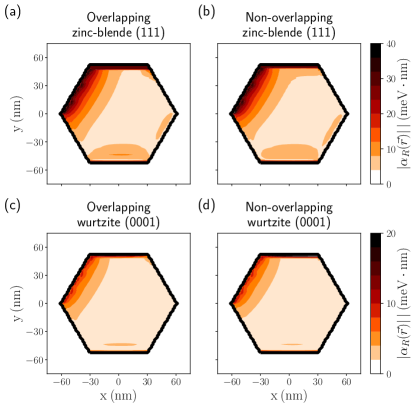
We note that the Rashba SO coupling is a position-dependent function because it depends on the gradient of the electrostatic potential . To better illustrate this dependence, in Fig. 6 we show calculations of the SO coupling for the two devices studied in this work (first column and second column) and for (111) zinc-blende (first row) and (0001) wurtzite (second row) InAs nanowires. The Rashba SO coupling in zinc-blende nanowires (top row) turns out to be roughly twice than in wurtzite crystals (bottom row). This has been pointed out in other theoretical works Campos et al. (2018); Escribano et al. (2020) and it is intimately related to the symmetries of both crystals. But in both cases, the spatial profile of the Rashba coefficient is the same. Particularly, the maximum is located at the Al/InAs interface, precisely where the charge density is maximum [see Fig. 7(c,d)], what benefits the topological protection of the states populating the wire. We also note that the maximum of the SO coupling is above 10 meVnm for both types of crystals (even for this small value), which is large enough to create a measurable topological gap.
In our simulations we have used the parameters that correspond to (111) zinc-blende nanowires, which are the typical ones used in experiments. However, (0001) wurtzite nanowires would have provided similar features (not shown), although with smaller topological minigaps.
Simplified model
The diagonalization of the Hamiltonian of Eq. (2) is computationally demanding because of the small grid spacing imposed by the large Fermi momentum of the Al layer. For this reason, we are only able to use this model to obtain the band structure and DOS for certain gate voltages, but not to compute the phase diagram of the studied devices in a broad range of parameters. To overcome this problem, we use a less demanding model that includes the induced pairing and exchange field in the wire in an heuristic way (as energy-independent but position-dependent parameters). This simplified model only considers the wire, and thus the effective Hamiltonian can be discretized using a larger lattice spacing ( nm in our simulations). In the following subsections we explain how both phenomena (the induced superconducting and magnetic effects) can be incorporated to reproduce qualitatively the behaviour of the full model.
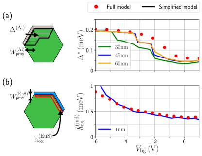
1. Induced superconductivity
We consider the superconducting proximity effect in the nanowire effectively by introducing a region close to the InAs/Al interface with a finite pairing amplitude [see sketch of Fig. 7(a)]. The parameter and the width of this proximitized region, , are then chosen such that this simplified model reproduces (approximately) the same behaviour for the induced superconducting gap as the full model.
In Fig. 7(a) we show the evolution of the induced gap versus the back-gate potential. Dots correspond to calculations using the full model while solid lines correspond to the simplified one. Different colors are used for different widths. We find that nm is the best fit to the full model results.
2. Induced exchange field
Following the same reasoning as for the induced pairing, we model the induced magnetization by introducing a region close to the InAs/EuS interface with a finite exchange field [see sketch in Fig. 7(b)]. Once again, we choose and the width of this proximitized region, , so as to reproduce approximately the results obtained with the full model. In Fig. 7(b) we show the mean induced exchange field versus the back-gate potential (where is the Fermi-Dirac distribution and is summed over all populated subbands ). Dots correspond to the full model calculations and solid lines to the simplified model using meV and nm. For the gate voltage range studied in this work (i.e. V) the simplified model provides a very good agreement with the full model. The characteristic penetration length of electrons into the insulating EuS is given (roughly) by the magnetic length
| (21) |
which is the value of the proximitized width that we use in our simplified model.
In addition to this direct proximity effect from the EuS into the InAs, there is an (ungateable) induced exchange field from the EuS into the Al of the order of 0.06 meV, see full-model calculations in main text. This proximity effect is present at the interfaces where Al and EuS overlap in the overlapping device (thus, it does not appear in the non-overlapping device). This effect causes an indirect proximity effect from the EuS into the InAs through the Al. We include this effect by adding an exchange field meV into the superconducting proximitized region discussed in the previous subsection.
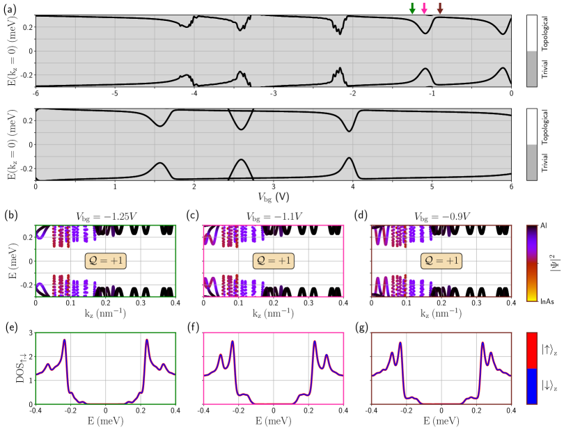
Topological phase diagram for the full model
In the main text we study the topological phase diagram (versus and ) using the simplified model. In this section we analyze the phase diagram versus the back gate potential using the full model, which is more computationally demanding. Note that is analyzed as a free parameter in the phase diagram of the simplified model, but it is a built-in quantity within the full model. This analysis complements the calculations performed in Figs. 2 and 3 of the main text.
In Fig. 8 we consider the case of the overlapping device. In panel (a) we show the energy spectrum at versus . For the voltage range shown there, we observe low energy pairs of states that cross zero energy at (roughly) V, V and V. These zero-energy crossings of the bulk states are related to topological phase transitions. This is demonstrated by the calculation of the topological invariant shown with white-grey colors (see the first section of this Supplemental Material for details on this calculation). In Fig. 8(b-d) we show the dispersion relation versus the momentum along the wire’s direction for three specific values: (b) at V, i.e., before the last topological region; (c) at V, inside the topological region; and (d) at V, after this region. In the top panel of these three figures we show with colors the weight of the states in the different materials, from a state completely located in the Al layer (black) to completely located in the InAs wire (yellow). The states that cross zero energy in this topological region correspond to mixed states with half of the wavefunction located in the Al and the other half in the InAs. For completeness, we also show in Fig. 8(e-f) the spin-polarized DOS for the bandstructures shown in Fig. 8(b-d).
We now perform the same analysis but for the non-overlapping device (see Fig. 9). We find that there are no topological regions for any value of , positive or negative, at least for the right-side gate voltage used in this simulation [see Fig. 9(a)]. This is because the induced exchange field in this device is much smaller than the induced gap [see Fig. 9(b-d)] and therefore no topological phase can be developed.
Topological phase diagrams for the simplified model versus side-gate potential
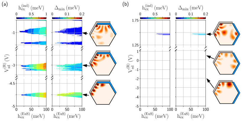
Using the simplified model, in the main text we study the topological phase diagram versus the back-gate potential. This gate not only tunes the chemical potential inside the wire, but it also moves upwards and downwards (along the axis) the charge probability density. This has a tremendous impact on this kind of heterostructure because, depending on the wavefunction position, the hybridization with the Al or the EuS layer dramatically differs. In the same way, the side gates play a similar role, but they change the position of the wavefunction along the perpendicular axis (the axis). Just by looking at the geometries of both devices (see Fig. 1 of the main text) one can infer that if the side gates push the wavefunction closer to the Fermi level towards the right part, the hybridization with the EuS will be increased while the hybridization with the Al will be suppressed.
To show this fact and to prove that the systems exhibit similar features in their topological phase diagrams regardless of whether the back gate or the side gates are tuned, we compute the topological phase diagram versus the right-side gate 555Note that, because right and left side gates are placed parallel to each other and symmetric with respect to the wire, they provide comparable phase diagrams.. We show the results in Fig. 10(a) for the overlapping device, and in Fig. 10(b) for the non-overlapping one. In the first two columns, we show with colors the topological regions (white means trivial, ). Particularly, colors in the first column correspond to the induced exchange field for the (topological) subband closest to the Fermi energy, and colors in the second column correspond to its minigap . In addition to this, we show on the right of each subfigure the probability density across the wire section of the lowest transverse subband (at ) at the value pointed with the arrows.
Let us discuss first the results for the overlapping device [Fig. 10(a)]. This geometry exhibits several topological regions that span across potential ranges of the order of mV. Increasing the right-side gate voltage for a fixed (see left panel) keeps the induced exchange field almost constant, while it decreases the minigap (see right panel). This is precisely because the lowest-energy wavefunction is being pushed towards the EuS layer, moving away from the Al layer (see charge density plots on the right).
In the non-overlapping device [Fig. 10(b)], we observe that there is no topological phase for negative right-side gate potential values. However, there are some small topological regions for positive gate potentials. This happens because the wavefunction is located close to the EuS layer for these gate potentials (see charge density plots on the right), acquiring a non-negligible induced exchange field. But due to the large doping of the wire, these states have a large kinetic energy, what implies that they spread all across the wire. Hence, both quantities, the induced exchange field and the minigap, are small or even negligible for these states.
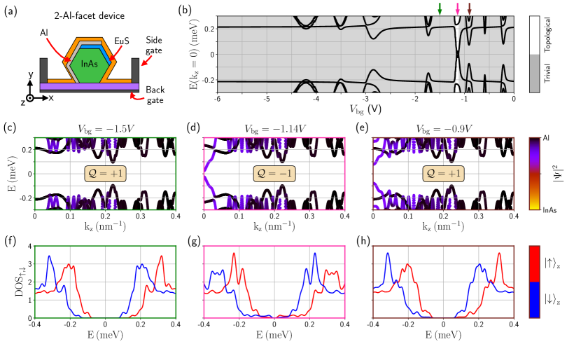
Two-Al-facet geometry
In this last section we consider a different geometry than those studied in the main text. This geometry was analyzed experimentally but didn’t provide zero bias peaks Vaitiekėnas et al. (2021). Strikingly, this device is identical to the overlapping device of Fig. 1(a) of the main text, but with an additional InAs facet covered by the Al shell [see Fig. 11(a) for a sketch]. In Fig. 11(b) we show the lowest energy spectrum versus the back-gate potential at . With grey/white colors we show whether the heterostructure has a trivial/non-trivial topological phase. For these gate voltages, there is only one topological region at (roughly) V. However, its extension and the size of its minigap are negligibly small, in sharp contrast to the overlapping device studied before. The bandstructure around this topological region is shown in (c-e). The lowest-energy states correspond to mixed states, but mainly located in the Al. More particularly, the lowest-energy wavefunction is mainly located at the left corner of the wire (not shown), where the band-bending of the superconductor leads to a larger accumulation of charge. This large hybridization with the superconductor is what suppresses the hybridization with the EuS, leading to a small exchange field induced directly in the InAs. And this in turn is what suppresses the appearance of topological states in this device.