Low-symmetry two-dimensional BNP2 and C2SiS structures
with high and anisotropic carrier mobilities
Abstract
We study the stability and electronic structure of previously unexplored two-dimensional (2D) ternary compounds BNP2 and C2SiS. Using ab initio density functional theory, we have identified four stable allotropes of each ternary compound and confirmed their stability by calculated phonon spectra and molecular dynamics simulations. Whereas all BNP2 allotropes are semiconducting, we find C2SiS, depending on the allotrope, to be semiconducting or semimetallic. The fundamental band gaps of the semiconducting allotropes we study range from eV to eV at the HSE06 level and display carrier mobilities as high as cm2V-1s-1. Such high mobilities are quite uncommon in semiconductors with so wide band gaps. Structural ridges in the geometry of all allotropes cause a high anisotropy in their mechanical and transport properties, promising a wide range of applications in electronics and optoelectronics.
Introduction
Two-dimensional (2D) materials have intrigued researchers around the world since the successful mechanical exfoliation of graphene [1]. Even though graphene remains unsurpassed in terms of high charge carrier mobility, the vanishing band gap in the pristine material precludes its use from semiconducting circuitry [2, 3]. Other 2D materials including transition metal dichalchogenides (TMDs) such as MoS2 have sizable band gaps, but are not as useful due to their low carrier mobility [4, 5]. Phosphorene, a monolayer of black phosphorus, combines high and anisotropic carrier mobility with a sizeable and tunable band gap [6, 7, 8], but is unstable under ambient conditions [9]. In spite of significant efforts to improve the performance of 2D materials in semiconducting devices, the progress has been moderate. There is a need to find new 2D semiconductors with substantial band gaps and high carrier mobilities.
Phosphorus carbide (PC), a recently proposed 2D material, has been predicted to be stable [10] and to display promising electronic behavior including high carrier mobility [11]. Of the stable allotropes, the semiconducting -PC phase, also called black phosphorus carbide (-PC), has been successfully synthesized. It shows a high field-effect mobility cm2V-1s-1 of holes at room temperature [12], good infrared response [13] and tunable anisotropic plasmonic performance [14]. The narrow band gap, however, limits the performance of PC-based field-effect transistors (FETs) due to a relatively low ON/OFF ratio [12]. Experimental data for 2D GeP [15], another low-symmetry IV-V compound with strongly anisotropic conductance, indicate a high field-effect ON/OFF ratio , but a low carrier mobility cm2V-1s-1. Theoretical explorations have been extended to other 2D IV-V compounds, which are not isoelectronic to PC. These include germanium triphosphide [16] GeP3, tin triphosphide [17] SnP3, and phosphorus hexacarbide [18] PC6. However, all these systems have narrow band gaps similar to -PC and share a hexagonal honeycomb lattice structure and thus a weak transport anisotropy. 2D structures with a substantial band gap, high carrier mobility and strong in-layer anisotropy are still missing.
In search of such 2D materials inspired by anisotropic 2D PC structures, we have applied an effective design strategy known as “isoelectronic substitution”. This process involves substituting certain elements in the structure by their neighbors in the periodic table, yet keeping the total valence electron count unchanged. This approach, which has been successfully applied in both 3D and 2D systems, allows to change physical and chemical properties of the system without drastically changing the structure. In this way, the diamond structure of bulk silicon with a diatomic unit cell can be changed to the isoelectronic Si3AlP, when one Si atom is substituted by Al and the other by P in every other unit cell, thus significantly increasing light absorption in the visible region [19]. In semimetallic 2D graphene with a diatomic basis, substituting one C atom by B and the other by N forms the -BN structure, a wide-gap insulator. In a similar way, substituting every other atom in phosphorene by Si and S atoms results in the 2D SiS structure [20, 21]. The same isoelectronic substitution in 2D group V systems leads to 2D group IV-VI compounds including GeS, GeSe, and SnS with a lower symmetry and a wide range of physical properties [22, 23, 24, 25].
In this study, we propose isoelectronic substitution in 2D structures of phosphorus carbide that leads to previously unknown ternary compounds BNP2 and C2SiS. Our ab initio density functional calculations identify four stable allotropes of each compound that share the 2D geometry with PC. Calculated phonon spectra and ab initio molecular dynamics (MD) simulations confirm the stability of each of these allotropes. Due to structural ridges in the geometry, all allotropes considered exhibit a significant anisotropy in the elastic response. Electronic structure calculations indicate that and phases of C2SiS, as well as all four BNP2 allotropes, are semiconductors with a wide range of band gap values. Carrier mobility calculations show that most of the semiconducting allotropes exhibit high and strongly anisotropic carrier mobilities. The remaining -C2SiS and -C2SiS allotropes were found to be semimetallic, displaying an elliptically distorted Dirac cone in their band structure caused by their structural anisotropy.
| BNP2 | C2SiS | |||||||
| (Å)a | 8.50 | 9.39 | 9.44 | 10.44 | 8.07 | 4.75 | 9.83 | 10.61 |
| (Å)a | 5.97 | 5.97 | 5.14 | 5.14 | 5.87 | 5.86 | 5.03 | 5.03 |
| (Å)b | 2.25 | 2.25 | 2.27h | 2.27h | ||||
| 2.24i | 2.23i | |||||||
| (Å)b | 1.78 | 1.78 | 1.79 | 1.79 | ||||
| (Å)b | 1.94 | 1.94 | 1.95 | 1.95 | ||||
| (Å)b | 1.40 | 1.40 | 1.46 | 1.46 | ||||
| (Å)b | 2.49 | 2.46 | 2.41h | 2.40h | ||||
| 2.35i | 2.35i | |||||||
| (Å)b | 1.77 | 1.77 | 1.77 | 1.77 | ||||
| (Å)b | 1.94 | 1.94 | 1.95 | 1.95 | ||||
| (Å)b | 1.36 | 1.36 | 1.42 | 1.42 | ||||
| (eV/atom)c | 4.74 | 4.74 | 4.98 | 4.98 | 5.25 | 5.26 | 5.54 | 5.54 |
| (eV/atom)d | -0.01 | -0.01 | -0.25 | -0.24 | 0.68 | 0.68 | 0.39 | 0.39 |
| (N/m)e | 7.17 | 40.59 | 10.24 | 57.53 | 6.42 | 33.79 | 14.89 | 53.35 |
| (N/m)e | 156.02 | 144.13 | 189.59 | 173.68 | 145.94 | 124.02 | 199.72 | 185.35 |
| (eV)f | 0.52 | 0.80 | 1.39 | 1.26 | 0.71 | 0.70 | 0.00 | 0.00 |
| (eV)g | 1.38 | 1.69 | 2.15 | 2.06 | 1.57 | 1.40 | 0.00 | 0.00 |
-
1
a and are the in-plane lattice constants defined in Fig. 1.
b is the equilibrium bond length between the respective species.
c is the cohesive energy per average atom with respect to isolated atoms.
d is the formation energy per average atom with respect to elemental structures.
e () are the 2D elastic constants along the () direction.
f -PBE is the band gap value at the DFT-PBE level.
g -HSE06 is the band gap value at the DFT-HSE06 level.
h Length of bonds within the structural plane.
i Length of bonds out of the structural plane.
Computational Techniques
We have used ab initio density functional theory (DFT), as implemented in the VASP code [26, 27, 28], throughout the study. We applied periodic boundary conditions, with 2D structures separated by a vacuum region in excess of Å. The reciprocal space was sampled by a fine grid [29] of -points in the Brillouin zone of 8-atom unit cells or its equivalent in supercells. We used projector-augmented-wave (PAW) pseudopotentials [30] and the Perdew-Burke-Ernzerhof (PBE) [31] exchange-correlation functionals. Selective band structure calculations were performed using the hybrid HSE06 functional [32, 33] with the default mixing parameter . We utilized the DFT-D2 [34] method to represent van der Waals (vdW) corrections to the total energy. We used a cutoff energy of 500 eV for the plane-wave basis set and considered the electronic structure to be converged once the total energy difference between subsequent electronic structure iterations would not exceed eV. All geometries were optimized using the conjugate-gradient method [35], until none of the residual Hellmann-Feynman forces exceeded eV/Å. The phonon calculations were carried out using the density functional perturbation theory [36, 37, 38], as implemented in the PHONOPY code [39]. The system dynamics was studied using canonical ab initio MD simulations with fs time steps. Our results are for supercells containing more than 100 atoms, which were kept at temperatures of K, K or K for periods exceeding ps.
Results and Discussion
Structure of BNP2 and C2SiS 2D allotropes
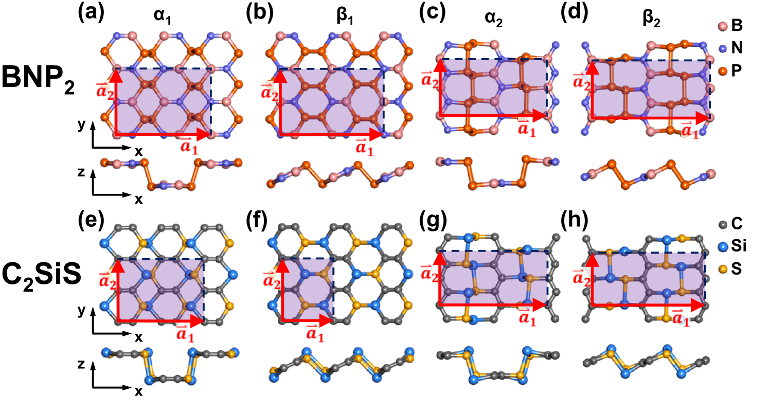
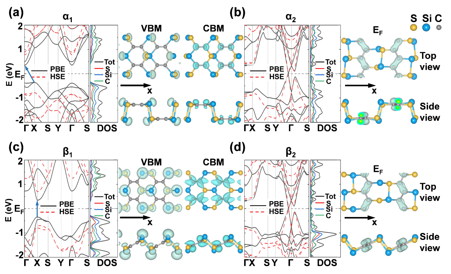
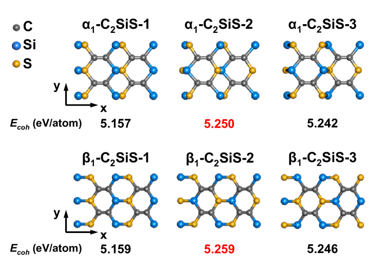
As introduced above, the 2D compounds BNP2 and C2SiS are isoelectronic to previously reported PC monolayer structures [10]. We have identified four 2D allotropes, called , , and , for each of the systems. The most stable structures of each allotrope are shown in Fig. 1. All atoms are 3-fold coordinated, causing a coexistence of and bonding and leading to structural ridges in the geometry of all allotropes. When viewed from the side, the allotropes have an armchair profile, whereas the allotropes have a zigzag profile. With the exception of -C2SiS with 8 atoms in the unit cell, all allotropes have rectangular unit cells containing 16 atoms. Additional metastable structures with different atomic arrangements in the unit cell are discussed in the Appendix.
As seen in Fig. 1, the optimized and allotropes of BNP2 structures consist of isolated P-P and B-N dimers forming a 2D hexagonal structure. Since the orientation of the B-N dimers alternates in the plane of the system, there is no net dipole moment in the system. P atoms prefer the configuration with a lone electron pair, whereas B and N atoms prefer the configuration in all BNP2 allotropes. The and allotropes represent two equivalent ways to achieve optimum configuration with the same topology, in analogy to black and blue phosphorene. [40]
The and allotropes of BNP2 contain alternating chains of P and BN along the -direction. The mismatch between the equilibrium P-P and B-N bond lengths leads to the formation of pentagon-heptagon pairs instead of hexagons.
The structure of all 2D allotropes of C2SiS closely resembles that of BNP2 due to the coexistence of -bonded C atoms and -bonded Si and S atoms. Similar to BNP2, the and allotropes of C2SiS contain isolated Si-S and C-C dimers. Also in this case, there are two distinguishable, topologically equivalent geometries. Even though the polar Si-S bonds are out of plane in this compound, their alternating orientation eliminates a net dipole moment. The and allotropes of C2SiS, analogous to those of BNP2, contain alternating C and SiS chains along the -direction. Bond length mismatch leads to a preferential formation of pentagon-heptagon pairs in the layer.
A summary of the structural characteristics and the cohesive energy of all these allotropes is presented in Table 1. In the BNP2 system, the B-N dimers in and allotropes are connected by typical double bonds with Å, close to the Å value in amino borane [41]. The bond length of the B-N chains in and allotropes is slightly longer, at about Å, close to the Å value in 2D -BN [42]. These results are consistent with the configuration of B and N atoms in 2D BNP2.
We find similar structural characteristics in the C2SiS system. As expected for -bonded C atoms, the C-C bond lengths are comparable to the double bonds in ethylene and the conjugated bonds in benzene or graphene. The length of all the other single bonds appears rather insensitive to the structure.
It is also noteworthy that P-N bonds are slightly shorter than P-B bonds in BNP2 due to the smaller atomic radius of the more electronegative element. The same is true, for the same reason, with the C-S bonds that are slightly shorter than C-Si bonds in C2SiS allotropes.
For the sake of easy comparison, we define the cohesive energy of an “average” atom by dividing the total atomization energy by the total number of atoms. Our results for are listed in Table 1. We found that for both BNP2 and C2SiS, and allotropes with the same index are almost equally stable. Our results also indicate that for both BNP2 and C2SiS, and allotropes are energetically more stable than and allotropes by eV/atom. We find the C2SiS structures to be generally more stable than BNP2 structures. The listed values of eV/atom here are comparable to cohesive energies found in PC monolayers [10].
We have further confirmed the stability of each allotrope by calculating the phonon spectra and by performing ab initio MD simulations. Details of all these calculations are presented in the Appendix.
We also calculated the formation energy per ‘average atom’ to investigate the relative stability of the ternary allotropes comparing with respect to their elemental components. We defined as
| (1) | |||||
where , , , are the respective total energies per average atom of the XlY compound and the elemental structures of X, Y and Z. In the particular case of 2D BNP2 and C2SiS structures, the elemental structures we consider are bulk boron, gas of N2 molecules, phosphorene, graphene, bulk silicon and bulk sulfur. The results of for all the allotropes are listed in Table 1. indicates instability and possibility of exothermic decomposition, whereas indicates stability.
Our results for in Table 1 indicate that all BNP2 allotropes are stable and will not decompose below K, at which point bonds may be broken. The values of for C2SiS allotropes considered here are positive, but rather small. The values eV/atom for the and phases and eV/atom for the and phases are an order of magnitude smaller than cohesive energies and comparable to eV/atom found in 2D-PC [10]. Structural changes would require overcoming a significant activation barrier associated with breaking bonds and protect C2SiS allotropes from structural changes at room temperature. As mentioned above, interatomic bonds may break and structural changes may become possible at extremely high temperatures of K. We find these estimates confirmed by our MD simulation results presented in the Appendix.
Anisotropic in-plane stiffness of 2D BNP2 and C2SiS allotropes
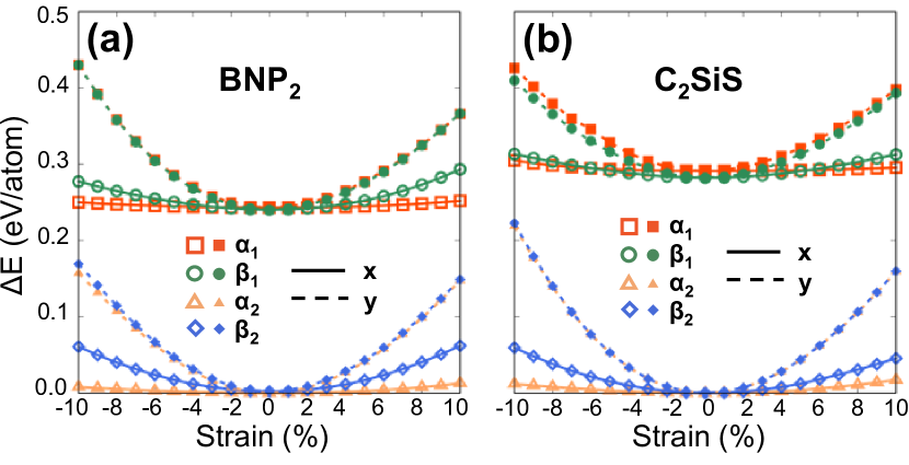
To investigate the elastic response of the 2D ternary structures, we subjected all allotropes in this study to in-layer uniaxial strain along the - and -direction and display differences of the average binding energy with respect to the most stable allotrope in Fig. 2. The presence of structural ridges renders all allotropes much softer along the -direction normal to the ridge direction. The allotropes of both BNP2 and C2SiS are particularly soft along the -direction, with 18 meV/atom when subjected to % compressive or tensile strain. The 2D elastic moduli [43] along the - and -direction, obtained using these calculations, are summarized in Table 1. For the semiconducting allotropes, these values play an important role in carrier mobilities.
Electronic structure of BNP2 2D allotropes
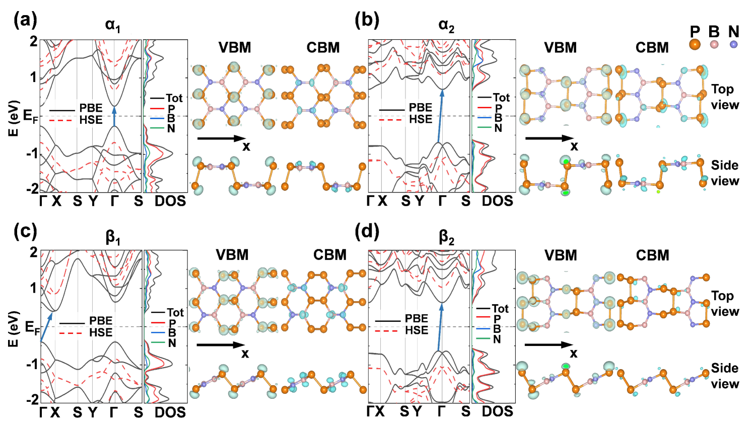
Results of our DFT calculations for the electronic structure of BNP2 monolayers are presented in Fig. 3. Our DFT-PBE results show all the four allotropes to be semiconductors. The fundamental band gap is direct in -BNP2 and indirect in all the other BNP2 allotropes. Band gap values based on DFT-PBE Kohn-Sham energies, ranging from eV to eV, are listed in Table 1. We should note here that the interpretation of Kohn-Sham eigenvalues as self-energies is strictly incorrect and that DFT-based band gaps are typically underestimated. We find this to be the case when comparing band gap values based on DFT-PBE and the hybrid DFT-HSE06 functional in Table 1. As seen when comparing band structure results based on DFT-PBE, given by the solid lines in Fig. 3, and DFT-HSE06, shown by the red dashed lines, the main difference is the opening of the fundamental band gap in DFT-HSE06, whereas the band dispersion is unaffected. We also present the total electronic density of states (DOS) and its projection onto the different species next to the band structure plots.
Contour plots of the projected DOS (PDOS) of all BNP2 allotropes at the valence band maximum (VBM) and conduction band minimum (CBM) are shown in Fig. 3, with the contributions to VBM and CBM distinguished by color. We find the character of the VBM to be dominated by the lone-pair states of the hybridized P atoms in all BNP2 allotropes. The character of the CBM is very different. The dominant contribution in and allotropes of BNP2 comes from out-of-plane orbitals of hybridized B and N atoms. In the and allotropes, orbitals of all the atoms contribute to the CBM character.
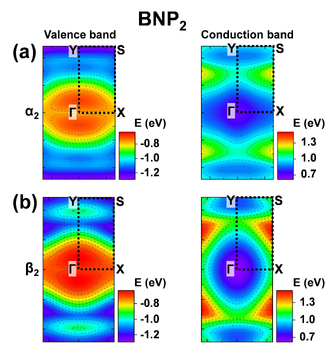
We also observe an unusually flat band in the band structure of and allotropes of BNP2 at the top of the valence region, along the line. To further explore the origin of this flat band, we show 2D contour plots of the dispersion within the top valence and bottom conduction bands in Fig. 4.
In both allotropes, the CBM energy minimum occurs at the point and the band dispersion around is almost isotropic and free-electron like. In contrast, the VBM is displaced from the point in the direction towards for both allotropes. Whereas the band dispersion is almost flat along the -direction, it is significantly higher along -direction near the VBM, indicating a significant anisotropy in the carrier effective mass. As seen in Fig. 3(b) and (d), this is caused at the VBM by a larger separation and lower hybridization between the P lone pair states along the -direction than along the -direction.
Electronic structure of C2SiS 2D allotropes
Results of our DFT calculations for the electronic structure of C2SiS monolayers are presented in Fig. 5. Our findings indicate that only the and the allotropes are semiconducting, whereas the and allotropes are semimetallic. The band gap is indirect in -C2SiS and direct in -C2SiS. Numerical band gap values based on DFT-PBE and DFT-HSE06 are listed in Table 1 and fall in the range of values found in BNP2.
According to Fig. 5, the character of VBM and CBM states in the semiconducting allotropes and is very similar. In analogy to results for BNP2, the VBM of C2SiS is dominated by lone-pair orbitals of Si atoms and the CBM contains mostly out-of-local-plane orbitals of C atoms.
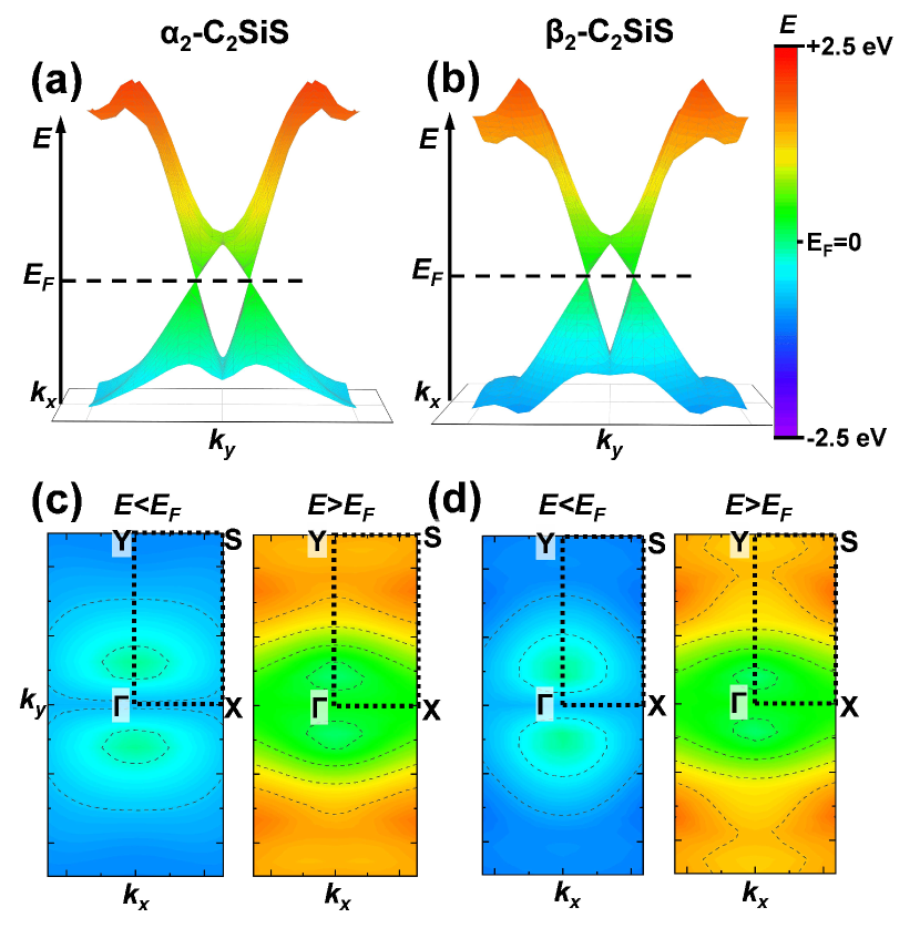
The and allotropes of C2SiS are found to be semimetallic by both DFT-PBE and DFT-HSE06. Dirac “cones” are seen in the band structure in Fig. 5(b) and (d), with the Dirac point at located between and in the Brillouin zone. The frontier states at are dominated by out-of-plane orbitals on C atoms.
The Dirac “cones” of - and -C2SiS are visualized in more detail in Fig. 6. The band dispersion in both allotropes is linear around , but anisotropic. As seen in Fig. 6(c) and (d), the cross-section of the “cone” at or is not a circle, but rather an ellipse elongated in the -direction. The higher steepness of the band dispersion along the -direction near the Dirac point is a consequence of a stronger interaction between C orbitals within zigzag chains of carbons, aligned with the -direction. These C chains in -C2SiS and -C2SiS are clearly visible in Figs. 1(g) and (h). Otherwise, these “cones” are very similar in Dirac point location, band dispersion and its anisotropy in both allotropes.
| a | a | b | b | c | c | ||
|---|---|---|---|---|---|---|---|
| () | (eV) | (103 cm2V-1s-1) | |||||
| -BNP2 | 0.51 | 0.34 | 1.36 | 0.40 | 0.40 | 151.21 | |
| 0.75 | 0.39 | 1.83 | 1.60 | 0.11 | 6.16 | ||
| -BNP2 | 0.67 | 0.34 | 0.69 | 1.37 | 5.89 | 10.51 | |
| 0.67 | 0.57 | 0.37 | 1.26 | 15.82 | 5.62 | ||
| -BNP2 | 0.88 | 0.78 | 1.01 | 0.88 | 0.30 | 8.29 | |
| 3.13 | 0.50 | 0.10 | 5.07 | 5.67 | 0.26 | ||
| -BNP2 | 0.53 | 0.75 | 2.41 | 0.68 | 0.65 | 17.17 | |
| 1.63 | 0.52 | 0.90 | 5.96 | 1.03 | 0.22 | ||
| -C2SiS | 0.53 | 0.28 | 0.39 | 1.37 | 4.38 | 15.66 | |
| 1.72 | 0.76 | 2.54 | 0.87 | 0.01 | 4.85 | ||
| -C2SiS | 0.14 | 1.57 | 2.51 | 6.31 | 1.69 | 0.09 | |
| 0.78 | 2.24 | 1.87 | 1.42 | 0.20 | 0.45 | ||
-
1
Electrons are denoted by and holes by .
a () are the carrier effective masses along the () direction.
b () are the deformation potentials along the () direction.
c () are the carrier mobilities along the () direction at K.
Carrier mobilities in semiconducting BNP2 and C2SiS 2D allotropes
Anisotropy in semiconducting BNP2 and C2SiS 2D allotropes is not only limited to the geometry, the elastic response and the electronic structure, but is also present in the carrier mobility. In absence of defects and external scattering centers, the mobility of carriers in 2D semiconductors is limited by acoustic phonons. We calculated the carrier mobilities of BNP2 and C2SiS 2D systems along the - and -direction using the deformation potential theory expression [44, 45, 11]
| (2) |
Here, represents the Cartesian direction, with standing for and for , and is the carrier charge. is the 2D elastic modulus [43] along the direction , obtained from the strain energy curve in Fig. 2. is the temperature, is the effective mass along the -direction, and is the average effective mass given by . The deformation potential along the -direction is determined at the valence band maximum (VBM) for holes and the conduction band minimum (CBM) for electrons. It is defined by , where is the energy shift of the band edge with respect to the vacuum level under a small change of the lattice constant . Our results for room-temperature carrier mobilities in all semiconducting 2D allotropes are summarized in Table 2.
We found that most allotropes in our study exhibit very high and remarkably anisotropic carrier mobilities. The highest carrier mobility value we found is cm2V-1s-1 for electrons in -BNP2 along the -direction, over two orders of magnitude higher than the value cm2V-1s-1 along the -direction. An important contributing factor to the mobility is the 2D elastic modulus [43]. The superior electron mobility along its -direction is a result of increased stiffness along this direction. According to Table 1, is indeed much larger than for most allotropes we study.
Unlike for electrons, hole mobility is highest along the -direction in , and allotropes of BNP2. The change of preferential transport direction is caused by substantial deformation potential anisotropy at the VBM according to Table 2. Carrier mobilities in semiconducting 2D allotropes of C2SiS are comparable to those in BNP2.
Carrier mobilities cm2V-1s-1 in -BNP2 with eV and cm2V-1s-1 in and allotropes of BNP2 with eV, evaluated at the PBE level of DFT are unusually high in view of the wide band gaps. This is particularly evident when compared to the values found in other similar 2D materials, as discussed in the Appendix. Even though these mobilities will be reduced due to inevitable defects and the interaction with the substrate under realistic conditions, we expect values in excess of cm2V-1s-1, which has been reported for phosphorene [6]. These results are very promising for the realization of 2D semiconducting devices with high ON/OFF ratios and on-state currents.
Summary and Conclusions
In summary, we have introduced previously unexplored 2D ternary compounds BNP2 and C2SiS as isoelectronic counterparts of 2D PC structures. Using ab initio density functional theory, we have identified four stable allotropes of each compound and confirmed their stability by calculated phonon spectra and molecular dynamics simulations. All allotropes display structural and elastic anisotropy due to structural ridges in their geometry, which are caused by coexisting and hybridization. Whereas all BNP2 allotropes are semiconducting, we find only two allotropes of C2SiS to be semiconducting. The other two allotropes of C2SiS are semimetallic and show anisotropic Dirac cones at . The fundamental band gaps of the semiconducting allotropes we study range from eV to eV at the PBE level and eV to eV at the HSE06 level of DFT. These 2D systems display carrier mobilities as high as cm2V-1s-1. Such high mobilities, with two orders of magnitude in anisotropy ratio, are desirable, but quite uncommon in semiconductors with so wide band gaps. Combination of wide band gaps with high and anisotropic carrier mobilities offer great promise for applications of 2D BNP2 and C2SiS structures in electronics and optoelectronics.
Acknowledgements.
This study was supported by the National Natural Science Foundation of China (NSFC) under Grant No. 61704110, the Fundamental Research Fund for the Central Universities, the Shuangchuang Doctoral Program of the Jiangsu Province, and by the Zhongying Young Scholar Program of Southeast University. D.T. acknowledges financial support by the NSF/AFOSR EFRI 2-DARE grant number EFMA-1433459. We thank the Big Data Computing Center of Southeast University for providing facility support for performing calculations presented in this manuscript.Appendix
Metastable structures of 2D BNP2 and C2SiS
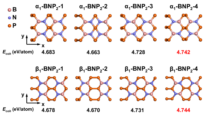
As seen in Fig. 1 of the main text, and allotropes of BNP2 contain four polar B-N dimers aligned with the -axis in each unit cell. Each of these dimer bonds may be rotated by 180∘. This gives rise to four metastable structures for -BNP2 and another four structures for -BNP2, shown in Fig. A1. The most stable structures among these, with the cohesive energy value highlighted in red, have been considered in the main text.
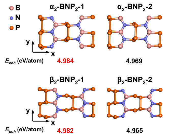
Quite different is the arrangement of B and N atoms in zigzag chains in the and allotropes of BNP2 shown in Fig. 1 of the main text. Also in this case, each bond may be rotated by 180∘. This gives rise to two metastable structures for -BNP2 and another two structures for -BNP2, shown in Fig. A2. Only the most stable among these allotropes have been considered in the main text.
Next we turn to the and allotropes of C2SiS, displayed in Fig. 1(e) and (f) of the main text. Unlike in BNP2, we can find only three inequivalent metastable structures for these systems, displayed in Fig. A3. For the and allotropes of C2SiS, optimization leads to only one stable structure. As for the other systems discussed above, we only consider only the most stable allotropes in the main text.
Phonon spectra of 2D BNP2 and C2SiS allotropes
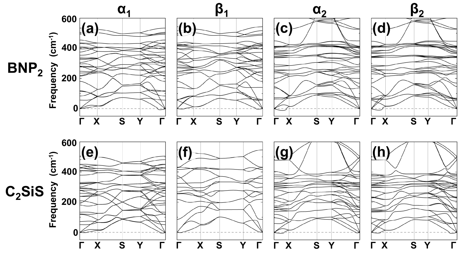
A real confirmation of structural stability, more important than a high cohesive energy, comes from the phonon spectra. Structures can be considered stable if no imaginary frequencies can be found in the phonon spectra. The calculated phonon spectra of all BNP2 and C2SiS allotropes discussed in this study are displayed in Fig. A4.
We should note at this point that phonon calculations for 2D structures with the uniquely soft flexural ZA mode are very demanding on precision [46]. We found our phonon spectra to be essentially free of imaginary frequencies associated with decay modes. The highest imaginary frequency value cm-1 in our spectra belongs to the ZA mode near the point in the Brillouin zone and is an artifact related to numerical precision [46].
Thermodynamic stability of 2D BNP2 and C2SiS allotropes
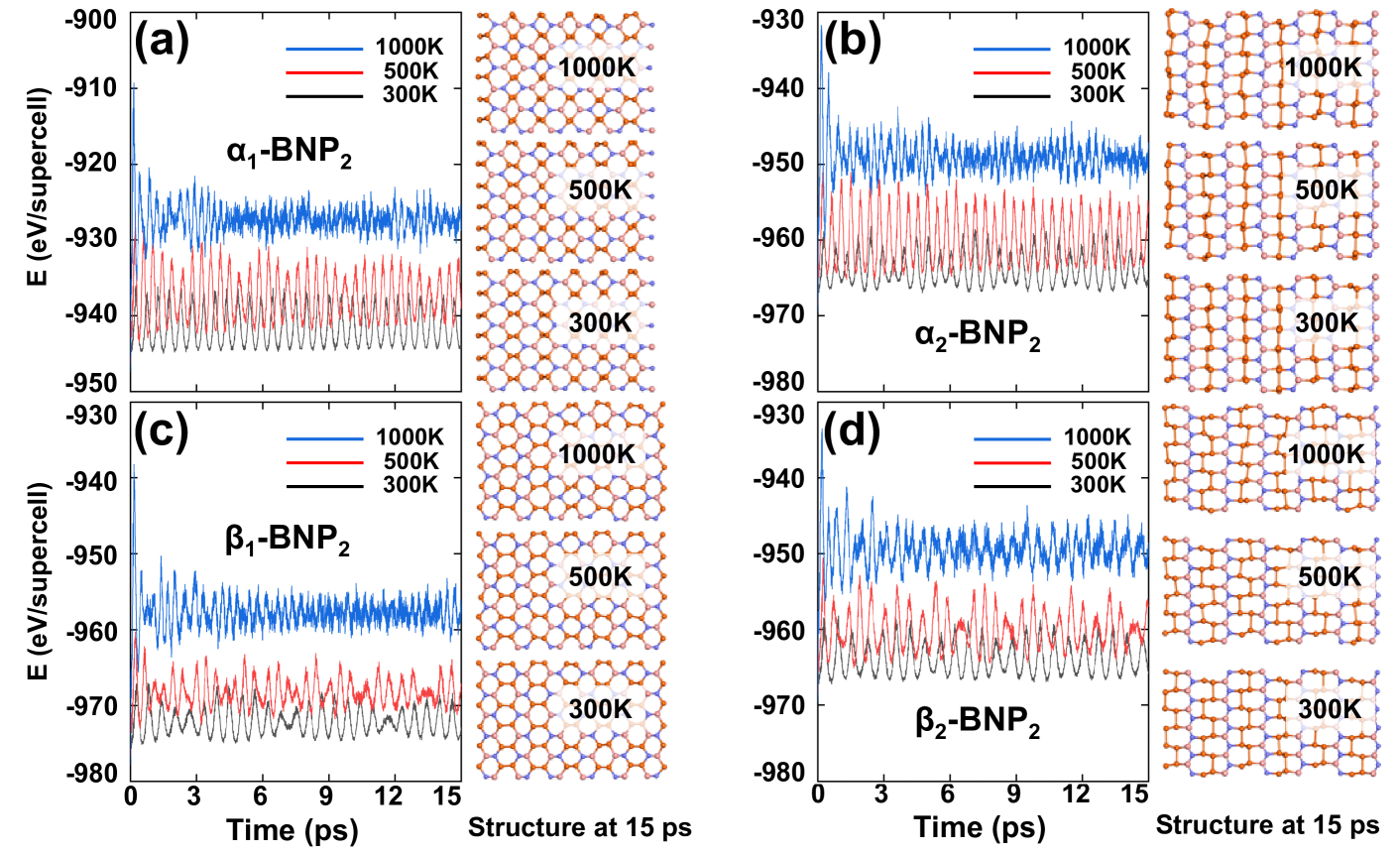
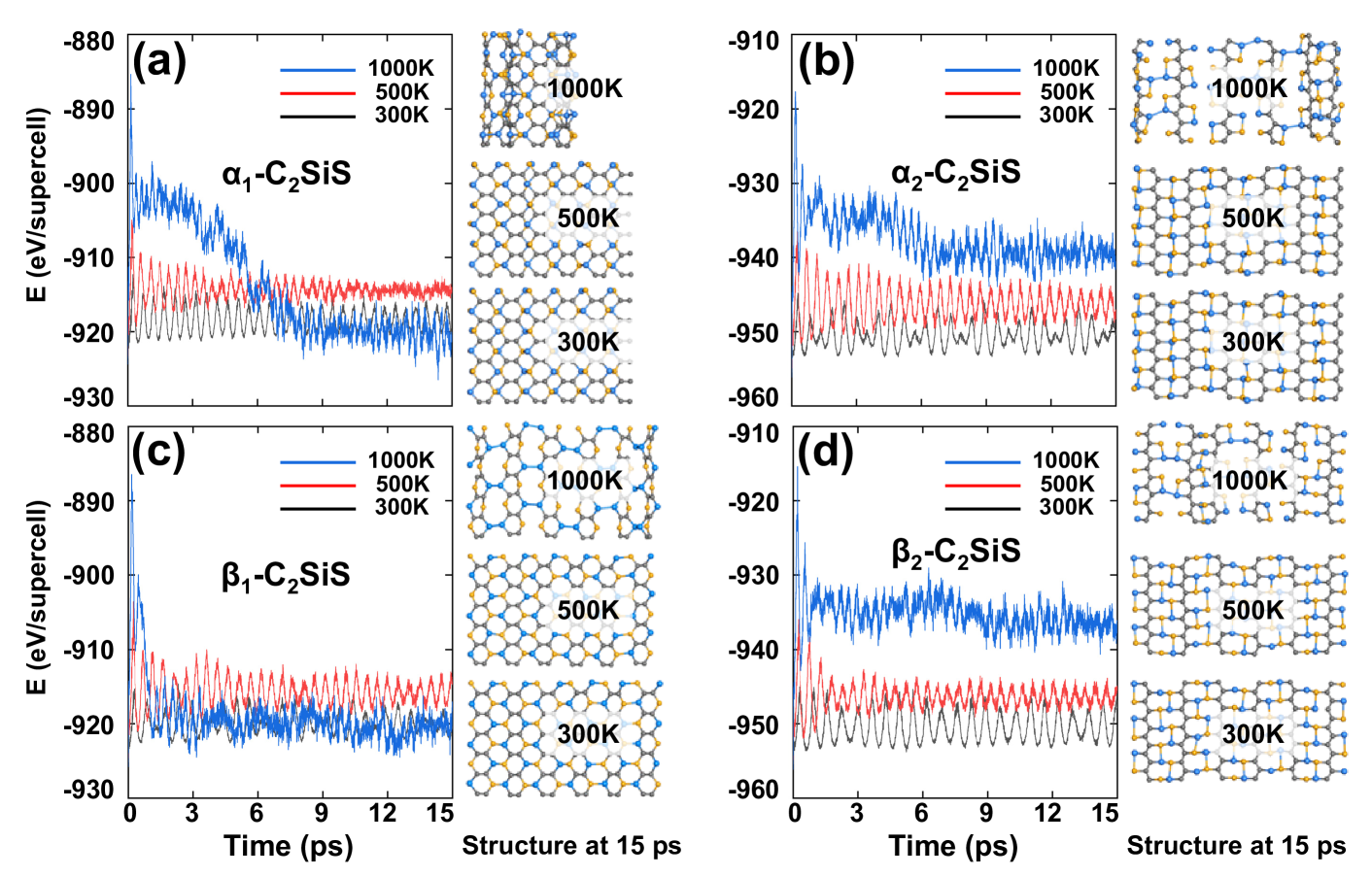
Whereas phonon spectra tell about structural stability in the harmonic regime, they cannot determine if a structure will or will not fall apart at a given finite temperature. To study the thermodynamic stability of the ternary structures in this study, we performed a set of canonical ab initio molecular dynamics (MD) simulations at K, K and K and present our results in Fig. A5 for 2D BNP2 and Fig. A6 for C2SiS structures. For ps long MD runs, we plotted both the fluctuations of the total potential energy and snapshots of the structures after ps.
Our results in Fig. A5 indicate that all four allotropes of BNP2 maintained their geometries up K, indicating a high thermodynamic stability. The corresponding results for C2SiS in Fig. A6 indicate all allotropes to be stable at K and K. Further increase of temperature to K causes a dramatic degradation of the and allotropes of C2SiS after ps. The and allotropes appear more stable at K, but their significant distortion indicates onset of degradation. The thermodynamic stability of all the BNP2 and C2SiS allotropes is either comparable to or superior to other similar 2D structures including GeP3 [16], which was shown to be stable at K, as well as PC [11] and binary V-V compounds [47], which were shown to be stable only up to K. Our MD results show good consistency with the conclusions obtained from the formation energy calculations discussed in the main text.
Suitability of BNP2 and C2SiS allotropes for electronic applications
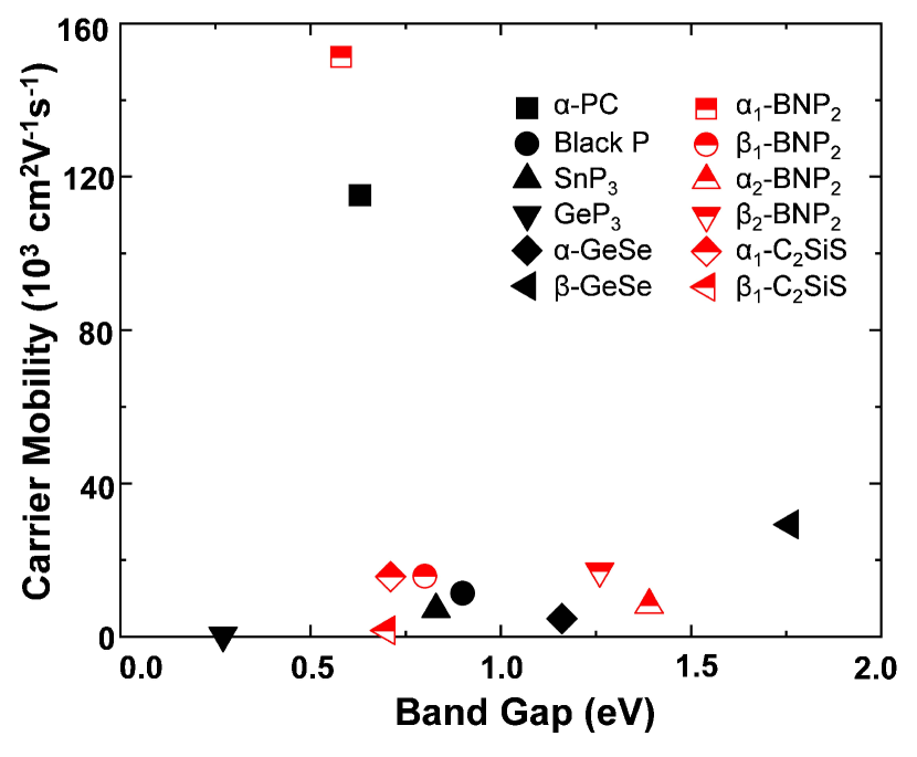
Combination of high carrier mobility and wide band gap is very desirable, as it results in a high ON/OFF ratio and a high on-state current in semiconductor devices. The 2D materials we introduce appear particularly suitable for electronic applications from that viewpoint. This is evidenced in Fig. A7, where we compare mobilities and band gaps of BNP2 and C2SiS to those of 2D-PC, GeP3 [16], SnP3 [17], black phosphorene, and 2D GeSe [48]. There is a general trade-off relation between carrier mobility and band gap. We find most of the BNP2 and C2SiS allotropes to be near the upper limit of the trade-off.
References
- Novoselov et al. [2004] K. S. Novoselov, A. K. Geim, S. V. Morozov, D. Jiang, Y. Zhang, S. V. Dubonos, I. V. Grigorieva, and A. A. Firsov, Electric field effect in atomically thin carbon films, Science 306, 666 (2004).
- Novoselov et al. [2005] K. S. Novoselov, A. K. Geim, S. V. Morozov, D. Jiang, M. I. Katsnelson, I. V. Grigorieva, S. V. Dubonos, and A. A. Firsov, Two-dimensional gas of massless Dirac fermions in graphene, Nature 438, 197 (2005).
- Zhang et al. [2005] Y. Zhang, Y.-W. Tan, H. L. Stormer, and P. Kim, Experimental observation of the quantum Hall effect and Berry’s phase in graphene, Nature 438, 201 (2005).
- Radisavljevic et al. [2011] B. Radisavljevic, A. Radenovic, J. Brivio, V. Giacometti, and A. Kis, Single-layer MoS2 transistors, Nature Nanotech. 6, 147 (2011).
- Fuhrer and Hone [2013] M. S. Fuhrer and J. Hone, Measurement of mobility in dual-gated MoS2 transistors, Nature Nano 8, 146 (2013).
- Liu et al. [2014] H. Liu, A. T. Neal, Z. Zhu, Z. Luo, X. Xu, D. Tománek, and P. D. Ye, Phosphorene: An unexplored 2D semiconductor with a high hole mobility, ACS Nano 8, 4033 (2014).
- Li et al. [2014] L. Li, Y. Yu, G. J. Ye, Q. Ge, X. Ou, H. Wu, D. Feng, X. H. Chen, and Y. Zhang, Black phosphorus field-effect transistors, Nature Nanotech. 9, 372 (2014).
- Wang et al. [2015] L. Wang, A. Kutana, X. Zou, and B. I. Yakobson, Electro-mechanical anisotropy of phosphorene, Nanoscale 7, 9746 (2015).
- Wood et al. [2014] J. D. Wood, S. A. Wells, D. Jariwala, K.-S. Chen, E. Cho, V. K. Sangwan, X. Liu, L. J. Lauhon, T. J. Marks, and M. C. Hersam, Effective passivation of exfoliated black phosphorus transistors against ambient degradation, Nano Lett. 14, 6964 (2014).
- Guan et al. [2016] J. Guan, D. Liu, Z. Zhu, and D. Tománek, Two-dimensional phosphorus carbide: Competition between and bonding, Nano Lett. 16, 3247 (2016).
- Wang et al. [2016] G. Wang, R. Pandey, and S. P. Karna, Carbon phosphide monolayers with superior carrier mobility, Nanoscale 8, 8819 (2016).
- Tan et al. [2017] W. C. Tan, Y. Cai, R. J. Ng, L. Huang, X. Feng, G. Zhang, Y.-W. Zhang, C. A. Nijhuis, X. Liu, and K.-W. Ang, Few-layer black phosphorus carbide field-effect transistor via carbon doping, Adv. Mater. 29, 1700503 (2017).
- Tan et al. [2018] W. C. Tan, L. Huang, R. J. Ng, L. Wang, D. M. N. Hasan, T. J. Duffin, K. S. Kumar, C. A. Nijhuis, C. Lee, and K.-W. Ang, A black phosphorus carbide infrared phototransistor, Adv. Mater. 30, 1705039 (2018).
- Huang et al. [2018] X. Huang, Y. Cai, X. Feng, W. C. Tan, D. M. N. Hasan, L. Chen, N. Chen, L. Wang, L. Huang, T. J. Duffin, C. A. Nijhuis, Y.-W. Zhang, C. Lee, and K.-W. Ang, Black phosphorus carbide as a tunable anisotropic plasmonic metasurface, ACS Photon. 5, 3116 (2018).
- Li et al. [2018] L. Li, W. Wang, P. Gong, X. Zhu, B. Deng, X. Shi, G. Gao, H. Li, and T. Zhai, 2D GeP: An unexploited low-symmetry semiconductor with strong in-plane anisotropy, Adv. Mater. 30, 1706771 (2018).
- Jing et al. [2017] Y. Jing, Y. Ma, Y. Li, and T. Heine, GeP3: A small indirect band gap 2D crystal with high carrier mobility and strong interlayer quantum confinement, Nano Lett. 17, 1833 (2017).
- Ghosh et al. [2018] B. Ghosh, S. Puri, A. Agarwal, and S. Bhowmick, SnP3: A previously unexplored two-dimensional material, J. Phys. Chem. C 122, 18185 (2018).
- Yu et al. [2019] T. Yu, Z. Zhao, Y. Sun, A. Bergara, J. Lin, S. Zhang, H. Xu, L. Zhang, G. Yang, and Y. Liu, Two-dimensional PC6 with direct band gap and anisotropic carrier mobility, J. Am. Chem. Soc. 141, 1599 (2019).
- Yang et al. [2012] J.-H. Yang, Y. Zhai, H. Liu, H. Xiang, X. Gong, and S.-H. Wei, Si3AlP: A new promising material for solar cell absorber, J. Am. Chem. Soc. 134, 12653 (2012).
- Zhu et al. [2015] Z. Zhu, J. Guan, D. Liu, and D. Tománek, Designing isoelectronic counterparts to layered group V semiconductors, ACS Nano 9, 8284 (2015).
- Yang et al. [2016] J.-H. Yang, Y. Zhang, W.-J. Yin, X. G. Gong, B. I. Yakobson, and S.-H. Wei, Two-dimensional SiS layers with promising electronic and optoelectronic properties: Theoretical prediction, Nano Lett. 16, 1110 (2016).
- Gomes and Carvalho [2015] L. C. Gomes and A. Carvalho, Phosphorene analogues: Isoelectronic two-dimensional group-IV monochalcogenides with orthorhombic structure, Phys. Rev. B 92, 085406 (2015).
- Gomes et al. [2015] L. C. Gomes, A. Carvalho, and A. H. Castro Neto, Enhanced piezoelectricity and modified dielectric screening of two-dimensional group-IV monochalcogenides, Phys. Rev. B 92, 214103 (2015).
- Fei et al. [2016] R. Fei, W. Kang, and L. Yang, Ferroelectricity and phase transitions in monolayer group-IV monochalcogenides, Phys. Rev. Lett. 117, 097601 (2016).
- Haleoot et al. [2017] R. Haleoot, C. Paillard, T. P. Kaloni, M. Mehboudi, B. Xu, L. Bellaiche, and S. Barraza-Lopez, Photostrictive two-dimensional materials in the monochalcogenide family, Phys. Rev. Lett. 118, 227401 (2017).
- Kresse and Furthmüller [1996] G. Kresse and J. Furthmüller, Efficient iterative schemes for ab initio total-energy calculations using a plane-wave basis set, Phys. Rev. B 54, 11169 (1996).
- Kresse and Hafner [1993] G. Kresse and J. Hafner, Ab initio molecular dynamics for liquid metals, Phys. Rev. B 47, 558 (1993).
- Kresse and Hafner [1994] G. Kresse and J. Hafner, Ab initio molecular-dynamics simulation of the liquid-metal–amorphous-semiconductor transition in germanium, Phys. Rev. B 49, 14251 (1994).
- Monkhorst and Pack [1976] H. J. Monkhorst and J. D. Pack, Special points for Brillouin-zone integrations, Phys. Rev. B 13, 5188 (1976).
- Kresse and Joubert [1999] G. Kresse and D. Joubert, From ultrasoft pseudopotentials to the projector augmented-wave method, Phys. Rev. B 59, 1758 (1999).
- Perdew et al. [1996] J. P. Perdew, K. Burke, and M. Ernzerhof, Generalized gradient approximation made simple, Phys. Rev. Lett. 77, 3865 (1996).
- Heyd et al. [2003] J. Heyd, G. E. Scuseria, and M. Ernzerhof, Hybrid functionals based on a screened Coulomb potential, J. Chem. Phys. 118, 8207 (2003).
- Heyd et al. [2006] J. Heyd, G. E. Scuseria, and M. Ernzerhof, Erratum: “Hybrid functionals based on a screened Coulomb potential” [J. Chem. Phys. 118, 8207 (2003)], J. Chem. Phys. 124, 219906 (2006).
- Grimme [2006] S. Grimme, Semiempirical GGA-type density functional constructed with a long-range dispersion correction, J. Comp. Chem. 27, 1787 (2006).
- Hestenes and Stiefel [1952] M. R. Hestenes and E. Stiefel, Methods of conjugate gradients for solving linear systems, J. Res. Natl. Bur. Stand. 49, 409 (1952).
- Baroni et al. [1987] S. Baroni, P. Giannozzi, and A. Testa, Green’s-function approach to linear response in solids, Phys. Rev. Lett. 58, 1861 (1987).
- Gonze [1995a] X. Gonze, Adiabatic density-functional perturbation theory, Phys. Rev. A 52, 1096 (1995a).
- Gonze [1995b] X. Gonze, Perturbation expansion of variational principles at arbitrary order, Phys. Rev. A 52, 1086 (1995b).
- Togo and Tanaka [2015] A. Togo and I. Tanaka, First principles phonon calculations in materials science, Scr. Mater. 108, 1 (2015).
- Zhu and Tománek [2014] Z. Zhu and D. Tománek, Semiconducting layered blue phosphorus: A computational study, Phys. Rev. Lett. 112, 176802 (2014).
- Sugie et al. [1979] M. Sugie, H. Takeo, and C. Matsumura, Microwave spectrum of aminoborane, BH2NH2, Chem. Phys. Lett. 64, 573 (1979).
- Şahin et al. [2009] H. Şahin, S. Cahangirov, M. Topsakal, E. Bekaroglu, E. Akturk, R. T. Senger, and S. Ciraci, Monolayer honeycomb structures of group-IV elements and III-V binary compounds: First-principles calculations, Phys. Rev. B 80, 155453 (2009).
- Liu et al. [2016] D. Liu, A. G. Every, and D. Tománek, Continuum approach for long-wavelength acoustic phonons in quasi-two-dimensional structures, Phys. Rev. B 94, 165432 (2016).
- Bardeen and Shockley [1950] J. Bardeen and W. Shockley, Deformation potentials and mobilities in non-polar crystals, Phys. Rev. 80, 72 (1950).
- Qiao et al. [2014] J. Qiao, X. Kong, Z.-X. Hu, F. Yang, and W. Ji, High-mobility transport anisotropy and linear dichroism in few-layer black phosphorus, Nature Commun. 5, 4475 (2014).
- Zólyomi et al. [2014] V. Zólyomi, N. D. Drummond, and V. I. Fal’ko, Electrons and phonons in single layers of hexagonal indium chalcogenides from ab initio calculations, Phys. Rev. B 89, 205416 (2014).
- Yu et al. [2016] W. Yu, C.-Y. Niu, Z. Zhu, X. Wang, and W.-B. Zhang, Atomically thin binary V-V compound semiconductor: A first-principles study, J. Mater. Chem. C 4, 6581 (2016).
- Xu et al. [2017] Y. Xu, H. Zhang, H. Shao, G. Ni, J. Li, H. Lu, R. Zhang, B. Peng, Y. Zhu, H. Zhu, and C. M. Soukoulis, First-principles study on the electronic, optical, and transport properties of monolayer - and -GeSe, Phys. Rev. B 96, 245421 (2017).