Reversible Fluxon Logic with optimized CNOT gate components
Abstract
Reversible logic gates were previously implemented in superconducting circuits
as adiabatic-reversible gates,
which are powered with a sufficiently slow clock.
In contrast, we are studying ballistic-reversible gates,
where fluxons serve to both encode the information and power the gates.
No power is applied to the gate apart from the energy of the input fluxons,
and the two possible flux polarities represent the bit states.
Undamped long Josephson junctions (LJJs),
where fluxons move at practically constant speed from inertia,
form the input and output channels of the gates.
LJJs are connected in the gates by circuit interfaces, which are designed
to allow the ballistic scattering from input to output fluxon states,
using the temporary excitation of a localized mode.
The duration of the resonant scattering determines the operation time of the gate,
approximately a few Josephson plasma periods.
Due to the coherent conversions between fluxon and localized modes
the ballistic gates can be very efficient:
in our simulations only a few percent of the fluxon’s energy are
dissipated in the gate operation.
Ballistic-reversible gates can be combined with other, non-ballistic gate circuits
to extend the range of gate functionalities.
Here we describe how the CNOT can be built as a structure that includes
the IDSN (Identity-else-Same-gives-NOT) and Store-and-Launch (SNL) gates.
The IDSN is a 2-bit ballistic gate, which we describe and analyze in terms
of equivalent 1-bit circuits.
The SNL is a clocking gate, that allows the storage of a bit
and the clocked launch of a fluxon on a bit-state dependent output path.
In the CNOT the SNL gates provide the necessary routing and
fluxon synchronization for the input to the IDSN gate.
Index Terms:
Ballistic signaling, fluxons, power efficient, reversible computing, superconducting logic circuits.I Introduction
Semiconducting logic greatly benefits from the dramatic scaling down of transistor gate and interconnect dimensions. Nowadays, however, the benefits from further scaling are nearly exhausted. This has direct implications for the characteristics of logic gates such as a gate’s energy cost: one of the bit states is stored as a voltage state on a capacitor, and the stored bit energy scales with the dimensions of the latter. In bit switching, which here amounts to discharging the capacitor, the entire energy of the stored bit state is dissipated. This energy cost is still much higher than the theoretical minimum energy cost, , incurred for every bit erasure in irreversible logic gates. In reversible logic gates, on the other hand, no bit erasure takes place. The ensuing absence of a fundamental lower bound of the energy cost motivated Bennett to develop a mathematical model for a reversible computer [1]. Later, Likharev described how classical reversible computing could be achieved in a superconducting circuit, using an external (clock) drive that adiabatically modulates the circuit potential [2]. The energy for bit switching is here proportional to the inverse of the gate time, and thus can theoretically be lowered indefinitely. More recently, such adiabatic-reversible gates have been realized with superconducting technology, in circuits named the Quantum Flux Parametron (QFP) [3] and the N-SQUID [4].
A physically different approach for energy-conservative computing is based on ballistic-reversible gates. In the classic model for these gates [5], logic operations are defined by the scattering of billiard balls. The gates are powered by the inertia of the input states (billiard balls) alone, in contrast to the external drive (clock) power used in the adiabatic model. Ballistic-reversible gates have been studied using optical solitons as information carriers [6, 7], however, these optical “particles” have been more thoroughly investigated for high-speed and long-distance communication [8].
We have previously proposed Reversible Fluxon Logic (RFL), which is designed to realize ballistic-reversible gates by the scattering of fluxons in special gate circuits [9]. The ballistic gates are unpowered other than the energy of the bit-representing fluxons. Also, the number of fluxons scattered in such a gate is conserved, and their energy is nearly conserved. However, the ballistic gates of RFL are not simply a realization of the billiard-ball model with fluxons, but have two main distinct features: (i) flux-polarity changes determine bit-switching in the gates instead of path changes, and (ii) the scattering processes which define the gate operation are resonant. The latter feature makes the gates both energy-efficient and fast, with gate duration set by a few natural JJ oscillation cycles.
| CMOS | Irreversible SFQ | Adiabatic-rev. SFQ | Ballistic-rev. RFL | |
|---|---|---|---|---|
|
bit states
1 & 0 |
voltage state
& null |
flux state
(SFQ) & null |
equiv. circulating
current states (e.g. CW & CCW) |
fluxon polarity
(topological charge) |
|
stored bit
energy |
charging energy |
JJ-switching energy |
(time-dependent) |
fluxon energy |
| energy cost |
per
bit switching |
per
switching JJ |
||
| power source |
voltage bias
|
current bias
|
(multi-phase)
current bias |
excess bit energy (e.g.
kinetic fl. energy) |
Table I compares different logic types in terms of their bit states, stored bit energy, energy cost, and power source. In CMOS (first column), the stored bit energy is given by the charging energy of a capacitance held at a source voltage . The capacitor is discharged during bit switching, and the entire charging energy is lost in the process. Similarly, in irreversible SFQ logic (e.g., RSFQ, ERSFQ, RQL) (second column) one bit state is represented by a single flux quantum (SFQ) stored at an energy . This is approximately equal to the energy cost of bit switching, which occurs under a phase slip of a damped JJ with critical current . For the bit states to be distinguishable, they must be separable by a potential barrier that is large compared to the energy of thermal fluctuations , thus requiring .
In contrast, reversible logic gates preserve a significant part of the stored bit energy. One approach to this in superconducting circuits are adiabatic-reversible gates (third column), where the bit-defining potential is slowly modulated by a clock. The two bit states are usually represented by circuit states of equal energy. During the transition from one bit state to the other the energy dissipated in the circuit scales inversely with the clock period [2] and thereby can be made arbitrarily small.
With RFL (fourth column) we follow the alternative approach of ballistic-reversible gates, which is based on the undamped motion of fluxons in long Josephson junctions (LJJs). A fluxon in an LJJ contains the flux of one SFQ, , and according to the sign (polarity) it is designated as either a fluxon or an antifluxon. The two flux polarities are used to represent the two bit states. Both bit states have the same stored bit energy, given here by the fluxon energy which is composed of the rest (potential) energy and kinetic energy. This stored bit energy can be adjusted for the application, similar to other superconducting SFQ technologies. Ballistic RFL gates make use of the scattering of fluxons at special circuit interfaces between LJJs. The fluxon’s rest energy and the fluxon number is conserved in the scattering. Moreover, as our simulations of the classical equations of motion of the RFL gate circuits show, the total fluxon energy is also conserved to a large extent. The remainder is lost to small-amplitude plasma waves generated by the fluxon at the gate.
Ballistic RFL gates developed so far have no internal state memory, in contrast to proposed asynchronous reversible gates [11, 12, 13]. That is why, ballistic gates for two or more input bits, such as the 2-bit NSWAP [9] and IDSN (Identity-else-Same-gives-NOT) gates [10], require a synchronous arrival of the input fluxons. In order to reliably use these gates as part of a larger circuit, we have therefore developed a gate for the purpose of clocking and synchronization. According to its operation it is named a Store-and-Launch (SNL) gate [10]. The gate stores the bit state of the incoming data fluxon as a static circulating current. Later, upon arrival of a low-energy clock fluxon, the state is launched as a fluxon with the same polarity as the original. The clock fluxon is the sole power source of the launch and is annihilated in the process. Part of its energy goes to the launched data fluxon which then may have larger energy than the (slowed-down) input data fluxon. The SNL can be designed with a clock fluxon, which has only a fraction of the data fluxon’s energy, and is therefore energy efficient by irreversible logic standards. Moreover, with SNL-clock fluxons as the main energy cost, while ballistic gates and LJJs as transmission lines are unpowered, RFL can avoid problems associated with the DC-biasing of JJs in irreversible SFQ logic [14, 15, 16].
The launch direction of the SNL is bit-state dependent: bit state 0 (fluxon) and bit state 1 (antifluxon) each have their designated output LJJ. This bit-state dependent routing adds an important resource to RFL logic. It allows to combine basic RFL components in a way that achieves a complex reversible gate operation, which for symmetry reasons cannot be achieved directly with a single ballistic RFL gate. As an example, we had proposed in Ref. [10] to implement a CNOT with a structure that is composed of several ballistic gates (including two IDSN gates) together with two SNL gates.
RFL was originally introduced in Ref. [9], where we studied fundamental ballistic gates of RFL through numerical simulation and also analytically with a collective coordinate model. In Ref. [10] we had extended the scope of RFL, by introducing concepts of the clocking gate SNL, the ballistic IDSN and the composite CNOT. These gates were however not studied in great detail and had not been optimized. Here we provide the missing details and extend the original study: for the IDSN we provide optimized parameters and margins, and also introduce an analytic model from which we derive parameter equivalences with 1-bit gates. We now introduce and study an SNL with two input LJJs, as is required in the CNOT application, while initially only a 1-input SNL version had been described [10].
This article is organized as follows: Firstly we summarize in Sec. II the operation of ballistic RFL gates and explain the resonant scattering dynamics in detail using the example of the simulated 1-bit NOT gate, Sec. II-A. The optimized 2-bit IDSN gate is described in Sec. III, where we show the simulated dynamics and analytically map the gate to equivalent 1-bit gates. Sec. IV presents the 2-input SNL gate with details of the dynamics and a comparison to an earlier 1-input SNL [10]. In Sec. V we describe the CNOT gate which is composed of the gates from the preceding sections.
II Short summary of ballistic RFL gates
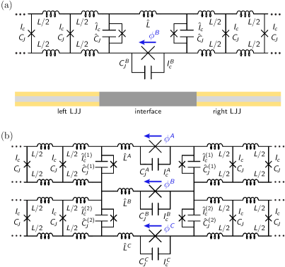
Long Josephson junctions (LJJs) are key structures in RFL. We design RFL circuits with discrete forms of LJJs, where an array of identical Josephson junctions (JJs) are connected by two inductor “rails”. In Fig. 1(a) two such discrete LJJs form the left and right parts of the circuit. The JJs have capacitance and critical current of , and each unit cell of length has the inductance . The circuit parameters set the Josephson plasma frequency , and the Josephson penetration depth, . The latter determines the length scale of phase gradients in the (discrete) LJJ, such as the width of a fluxon or edge states at the LJJ boundaries.
A fluxon in an LJJ is described by the soliton solution of the Sine-Gordon equation for the superconducting phase field . According to that solution, the fluxon behaves like a relativistic particle, moving with constant speed below the upper velocity bound . The energy of the moving fluxon is increased by a factor
| (1) |
relative to its rest energy , where .
In a discrete LJJ, the discreteness introduces a damping of the fluxon motion, compared to its motion at constant speed in a continuous LJJ. The strength of this perturbation is determined by the relative discreteness . In our circuit simulations, we choose to be sufficiently small, such that the loss in speed (and energy) is negligible even when the fluxon moves over hundreds of unit cells.
The bit-switching mechanism of the logic requires a method to invert the fluxon polarity. The 1-bit NOT gate, as the fundamental realization for bit-switching, is implemented in a circuit as shown in Fig. 1(a), where an input LJJ and output LJJ are connected by a circuit interface. The designation as input and output LJJs can in principle be reversed since the circuit has left–right symmetry. The interface consists of at least three capacitively shunted JJs (CSJJs). Each LJJ is terminated by a CSJJ with parameters between its inductor rails, and we call these the left and right ‘termination-JJs’ of the interface. The two rails of one LJJ are connected to those of the other, where one connection (shown between the lower rails) is formed by a CSJJ with parameters , and we call it the ‘rail-JJ’ of the interface. The other connection (shown between the upper rails) is made with an inductor that is typically small () and the interface cell thus cannot store a flux quantum.
Depending on the interface parameters, such a circuit interface has been found to enable forward-scattering of an incoming fluxon from one LJJ to the other [9]. In these processes the incident fluxon breaks at the interface into two parts, where its characteristic phase and current distributions become discontinuous. Its energy is transferred to excitations of the interface JJs and evanescent fields in the LJJs close to the interface. These localized excitations undergo a short coherent oscillation before a new fluxon forms in the other LJJ. Importantly, for certain interface parameters the polarity of the newly created fluxon is opposite to that of the original fluxon, and thus realizes a NOT gate. We note that polarity inversion is not possible for a fluxon within the bulk of a planar LJJ due to its topological nature (other than by a wiring crossover for a half-twist in an LJJ, not used here). In contrast, in the NOT gate the polarity inversion is possible due to the interface’s rail-JJ, which opens the otherwise flux-impermeable LJJ rails and allows for a large difference of building up between the left and right termination-JJ phases. This phase change is dissipationless, unlike phase switching in the resistively shunted JJs of SFQ logic gates or in overdriven unshunted JJs. In subsection II-A below we describe the NOT gate operation in more detail.
For the purpose of ballistic gates, the parameters of the interface cell are set such that the fluxon scattering is resonant. By resonance we mean that the energy transfer from the moving fluxon to the localized excitation and again to a moving fluxon happens coherently. Considering the highly nonlinear nature of the fluxons and other involved modes, no obvious and unambiguous resonance criterion in the sense of matching frequencies exists. At resonance, the gate is particularly efficient since energy loss through plasma waves generated at the interface is minimized. Correspondingly, the energy-efficiency of the gate (ratio of fluxon energy before and after the scattering) assumes a local maximum with respect to most interface parameters, cf. Fig. 9 in Ref. [9]. For example, a resonant NOT gate requires relatively large shunt capacitances of the three interface JJs [9, 17].
Different types of scattering resonances can be observed at different points in parameter space, each within a finite (but wide) range around an efficiency maximum. They can be classified according to characteristics such as (i) the number and duration of the interface oscillation cycles (comparable to the ‘bounces’ in LJJs with point defects [18]). Furthermore, (ii) a resonance may preserve or invert the polarity of the incoming fluxon, and (iii) the new fluxon may be created in the output LJJ (forward-scattering) or in the input LJJ (backward-scattering). For a given set of interface parameters, the resonant scattering typically is observed within a range of fluxon input velocities . In the adiabatic limit, i.e. for very small input velocity, , the flux quantum will be lost in the gate. In contrast, in adiabatic-reversible logic the clock can be slowed in principle to an arbitrarily small frequency.
Similar to the 1-bit NOT gate, a ballistic 1-bit Identity (ID) gate can be implemented with the structure in Fig. 1(a), using a specific set of interface parameters. The fluxon induces at the ID gate interface a different resonance compared to the NOT gate resonance, and from it a new fluxon is created in the output LJJ which has the same polarity as the input fluxon. This resonant ID gate can in principle be parametrically tuned into a NOT gate, since both fundamental 1-bit gates are based on the same circuit-interface structure. This is an advantage over a trivial ID operation in form of non-resonant transmission, e.g. through a regular LJJ cell, and informs the construction of more complex gates from the fundamental 1-bit gates. We have for example designed ballistic 2-bit gates based on the circuit structure shown in Fig. 1(b). It has two input and two output LJJs connected by a circuit interface with 7 CSJJs. Interface parameters are set such that a fluxon coming in on the upper (lower) input LJJ is scattered forward to the upper (lower) output LJJ. In these 2-bit gates the polarity inversion is conditional: depending on the interface parameters and on the presence and polarity of a synchronized input fluxon on the other LJJ, the action on the bit is polarity-preserving or polarity-inverting. So far, ballistic RFL designs exist for a 2-bit NSWAP=NOT(SWAP) logic gate [9], and for an IDSN logic gate [10]. An updated version of the latter is discussed in detail in Sec. III.
The dynamics of the JJ phases in a given circuit is obtained through numerical integration of the classical circuit equations of motion, with fluxon(s) moving in the input LJJ(s) taken as initial conditions. For a desired gate operation, we identify suitable interface parameters by optimization of the gate efficiency. Parameter variations around these optimized values generally show relatively robust parameter margins [9], suggesting the feasibility of the gates in fabrication and operation. If the interface parameters are chosen far away from the parameter range set by these margins, the resulting dynamics in general are not useful as an RFL gate, such as fluxon annihilation or reflection. In certain limits far away from our gate margins, the fluxon dynamics at the interface is comparable to other well-studied fluxon phenomena, e.g. scattering of a fluxon at an LJJ end with specific boundary condition [19, 20], or scattering within the LJJ at a perturbation potential. The latter, which include the resonant chaotic scattering at point defects [18, 21] and fluxon scattering at a qubit-induced potential [22], do not allow polarity change. The interface scattering used in RFL gates is non-perturbative, since the fluxon breaks up and loses its identity at the interface.
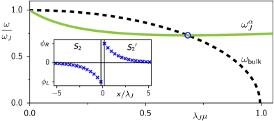
II-A Dynamics in the 1-bit NOT gate
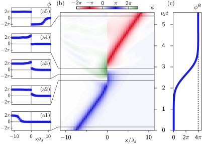
Fig. 2 shows the dynamics of a ballistic NOT gate, in the circuit of Fig. 1(a). We obtain the evolution of the JJ phases from the simulation of the circuit equations of motion. The simulation starts from an initial phase distribution corresponding to a fluxon that moves in the left LJJ () with velocity towards the interface at . (Note that other simulations include also a circuit structure for launching fluxons [9].) The JJ phases in the left and right LJJ, including those of the left and right termination JJs of the interface, are shown in the panels of subfigure (a), each taken at a particular time of the dynamics. Subfigure (b) shows the evolution of as a continuous function of time; the colormap emphasizes phases close to the values () of largest Josephson energy. Subfigure (c) shows the evolution of the interface’s rail-JJ phase .
In panel (a1) one sees in the left LJJ the still undisturbed fluxon, with characteristic phase profile varying in position from to (for fluxon with positive polarity). Panels (a2)–(a4) illustrate the situation after the fluxon has broken up at the interface and induced an excitation of the interface JJs and adjacent JJs. This excitation has the form of exponentially localized edge states in the two LJJs. When the fluxon breaks up (at a time just before that shown in panel (a2)) the phase profiles left and right of the interface have negative, fluxon-like slopes: from in the fluxon’s wake in the left LJJ at to near the interface, and from near the interface to in the right LJJ at . These phase distributions then undergo coherent amplitude swings, stills of which are shown in panels (a2)–(a4). The oscillations left and right of the interface occur around and , respectively, with maximum amplitudes of , and with evolving phase difference between the two. During the oscillations the LJJ phase distributions close to the interface change their character from fluxon-like (negative slope) to antifluxon-like (positive slope). When the slope to the right of the interface turns from negative in panel (a3) to positive in panel (a4), this may be seen as the starting point for the formation of an antifluxon. The phase distribution in the right LJJ develops into that of an antifluxon, varying from at the interface to in the bulk of the right LJJ. All along, the growing phase gap between right and left LJJ is compensated by the likewise growing phase of the interface’s rail-JJ, , cf. subfigure (c), while the small inductance in the interface cell stores negligible flux. By the time when has grown close to , the antifluxon is released from the interface into the right LJJ where it moves freely, as shown in panel (a5). The -phase change is adiabatic, happening on the time scale of the Josephson period, , in contrast to the rapid (and dissipative) -phase slips in RSFQ logic.
In subfigure (b) one can see the evanescent phase fields excited around the interface during the resonant process. The coherent oscillation of these edge states is characteristic for the resonant fluxon scattering used in RFL. A related ‘bounce’-resonance can be observed in an LJJ when a fluxon is scattered at a point defect such as a locally modified critical current [18]. Subfigure (b) also shows that small plasma waves are emitted into the LJJs during and after the scattering process. They carry away a fraction of the initial fluxon energy. However, as indicated by the indistinguishable trajectory slopes of the incoming fluxon and outgoing antifluxon, this is only a minor loss: from fluxon fits before and after the scattering we see that 97% of the fluxon energy is conserved.
III The IDSN gate
We had recently introduced a type of ballistic 2-bit gate, which is named IDSN after the operations it performs: a single input fluxon undergoes an ID operation, and two synchronized fluxons of the same polarity each undergo a NOT operation [10]. Table II summarizes the logic action of the IDSN gate. Note that the IDSN is a conditionally reversible gate [23, 24], where only certain 2-bit inputs are allowed, while all 1-bit inputs are allowed. Like the previously introduced NSWAP gate, the IDSN gate is implemented by the resonant fluxon scattering at a gate interface of the type shown in Fig. 1(b). The circuit has left–right symmetry across the interface, as well as vertical symmetry about the B-rail, i.e. , , , and , , see also Fig. 3(a). Within certain ranges of the interface parameters, this structure supports an IDSN gate. Similar to other ballistic gates that make use of the resonant forward-scattering, it requires specific, large (shunt) capacitances for the interface JJs. Unlike the NOT, ID, and NSWAP ballistic gates, the IDSN uses interface JJs which also have relatively large critical currents . For example, the particular IDSN gate of Ref. [10] has parameter values , , and , while the geometric inductances in the interface are negligible, . Here we present a new IDSN gate with non-negligible interface inductance . The parameters are given in the caption of Fig. 3. The new IDSN differs in the details of the resonance dynamics from the one discussed in Ref. [10]; moreover, it has improved margins compared with the latter.
| Input | Output | ||
| LJJ | LJJ | LJJ | LJJ |
| – | – | – | – |
| 0 | – | 0 | – |
| – | 0 | – | 0 |
| 1 | – | 1 | – |
| – | 1 | – | 1 |
| 0 | 0 | 1 | 1 |
| 1 | 1 | 0 | 0 |
The fluxon dynamics for this new IDSN is shown in Fig. 3(b-d). Subfigures (b) and (c) illustrate the dynamics for a single fluxon which is coming in on input LJJ and input LJJ , respectively. The dynamics for these two initial conditions is of course equivalent, owing to the vertical symmetry of the structure. In either case, the incoming fluxon creates a short resonant excitation centered at the interface from which a new fluxon is created in the corresponding output LJJ, and , respectively. The output fluxon has the same polarity as the input fluxon, similar to the 1-bit ID gate. However, the resonance here consists of a longer oscillation cycle at the interface than in the optimized 1-bit ID gate, cf. Fig. 2 in Ref. [9]. The different dynamics in the IDSN can be attributed to the additional excitation of interface rail-JJs and evanescent field excitation in the non-fluxon carrying LJJs, see analysis in Sec. III-A.
Subfigure (d) shows the scattering dynamics for two synchronized fluxons, each coming in on its own input LJJ. Here the dynamics in the upper and lower part of the structure is dynamically decoupled, because the current across the rail-JJ with phase cancels due to symmetry reasons. This is similar to the NSWAP gate with input fluxons of equal polarity, and as in that case the fluxons here also undergo NOT dynamics, i.e. they are forward-scattered to the output LJJs with inverted polarity. Owing to the decoupled dynamics in upper and lower half, the resonance here is essentially identical to that of the 1-bit NOT gate, with however slightly different gate duration and efficiency. These differences are due to the deviation from the optimized parameters of the 1-bit NOT, required here (as in 2-bit gates in general) for a compromise with the other IDSN operations.
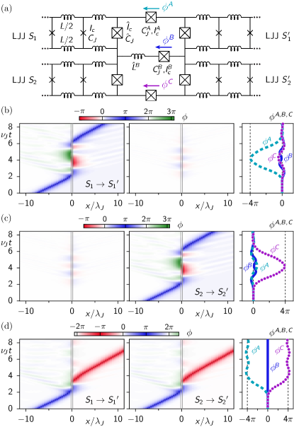
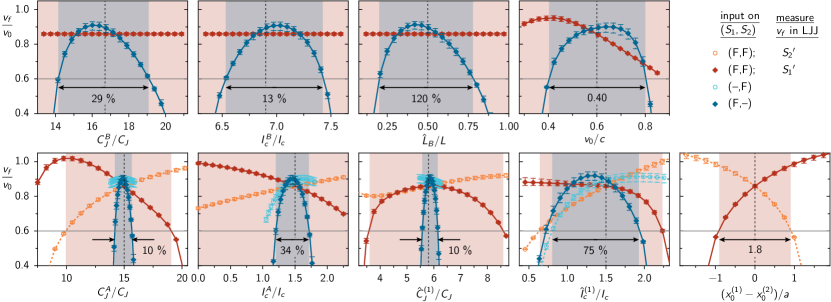
Fig. 4 summarizes the robustness characteristics of the IDSN gate with respect to variations of the interface parameters and the initial state. The individual panels of Fig. 4 show the ratio of output-to-input velocity of the forward-scattered fluxon(s) vs. the varied parameter, both for the single-fluxon processes (blue and light blue) and the two-fluxon processes (red and orange). Each panel shows the effect of one parameter variation around the optimized value (given in the caption of Fig. 3 and indicated here by vertical dashed lines), while all other parameters of the system are held fixed. The parameter variations shown in the first row of panels preserve the top-bottom symmetry of the interface (variation of ) or of the initial condition in the LJJs (equal variation of the fluxon input velocities in both LJJs, ). Accordingly, the fluxon output velocity is here independent of whether the fluxon is sent in on input LJJ or in the single-fluxon process. Similarly, is equal in both output LJJs and in the two-fluxon process. That is why only two data lines are seen in the first row of panels. In contrast, the parameter variations shown in the second row of panels break either the top-bottom symmetry of the interface (variation of ) or the top-bottom symmetry of the initial condition in the LJJs (variation of relative initial fluxon position for double-fluxon process). In these cases it therefore makes a difference whether a single fluxon is sent in on LJJ and measured in (dark blue diamonds) or sent in on LJJ and measured in (light blue circles). Similarly, in the two-fluxon process the output velocities measured on (dark red diamonds) and (orange circles) differ.
The shaded regions in Fig. 4 show the ranges where is fulfilled, for either two-fluxon input (red shaded) or single-fluxon input (blue shaded), corresponding to an energy efficiency of , cf. Eq. (1). The margins resulting from this efficiency criterion are indicated by the arrows. Given current fabrication uncertainties, these margins are sufficiently wide to allow fabrication and testing. The interface parameters that need to be defined most precisely, within 10%, are the capacitances of the upper and lower rail-JJs of the interface, and the capacitances of the left and right interface JJs. In the two-fluxon process also the input fluxons need to be relatively well synchronized, with a delay time less than at velocity , corresponding to an admissible separation less than cells between the two fluxons. The range of acceptable input velocities, , is conveniently wide, despite the resonant character of the underlying dynamics. This is different from the chaotic character of resonant scattering at point defects in LJJs [21].
III-A Equivalent 1-bit gate circuits
We now briefly discuss how the IDSN gate operations are dynamically equivalent to certain 1-bit interfaces, depending on the input type. The resulting mappings to approximately equivalent 1-bit interfaces are summarized in table III for the IDSN gate of Fig. 3. Similar reductions of the 2-bit gate dynamics have been discussed for the input cases of the NSWAP gate [9].
(i) When two fluxons of the same polarity approach the vertically symmetric 2-bit interface at the same time, the currents excited in the rails of the interface form a vertically antisymmetric distribution, and the current through the center rail cancels. The dynamics in the upper and lower part of the interface is then effectively decoupled, and in each of them is equivalent to the dynamics of a 1-bit interface as shown in the left column of table III. The 1-bit interface has only a single rail-JJ, which is identical to one of the outer-rail JJs of the 2-bit interface, with parameters .
(ii) Consider a single fluxon coming in on the upper input LJJ . It dominantly excites the upper part of the IDSN structure, where the upper rail JJ starts winding by more than . Due to the current conservation on the interface rails, current also flows in the lower part of the interface. The resulting phase fields in the lower LJJs, and , have the form of exponentially localized edge states, and their amplitude remains small, . This allows us to approximately map the gate dynamics to that of a fluxon scattering in the 1-bit circuit shown in the right column of table III. In this mapping each of the lower LJJs , of the IDSN, including its termination JJ with parameters , is replaced by a single effective JJ, with characteristics,
| (2) | |||||
where is the inverse decay length () of the edge states. These quantities are derived in the Appendix, where we parametrize the LJJ fields by exponentially localized edge states, and thus reduce the many degrees of freedom of each LJJ together with its termination JJ to the amplitude of the edge state. Furthermore, by comparing the plasma frequency of the effective JJ, , with the frequency with which the edge states oscillate in the LJJ bulk, we can estimate . The resulting values from Eq. (2) are given in the right column of table III.
We have simulated the fluxon scattering dynamics of the equivalent 1-bit interfaces in table III. In case (i) (left column of table III), where the reduction is exact due to symmetry, there is of course full agreement with Fig. 3(d). In case (ii) (right column of table III), although the reduction is only approximate, it nevertheless leads to excellent agreement between the 2-bit gate dynamics, as is seen in the comparison between Fig. 3(b) and Fig. 8.
| Two synchronized fluxons (same polarity) | Single fluxon |
![[Uncaptioned image]](/html/2010.15991/assets/figure_inksketch_IDSN_twofluxons.png) |
![[Uncaptioned image]](/html/2010.15991/assets/figure_inksketch_IDSN_onefluxon.png) |
|
e.g. with parameters
A,C-rail: , B-rail: , , |
|
| Equivalent 1-bit interfaces: | |
![[Uncaptioned image]](/html/2010.15991/assets/figure_inksketch_IDSN_twofluxons__equivBB1.png) |
![[Uncaptioned image]](/html/2010.15991/assets/figure_inksketch_IDSN_onefluxon__equivAA1BB4JJsquid.png) |
| , | , , , |
IV A store and launch (SNL) gate
The IDSN gate is an example of a ballistic 2-bit gate, with an energy efficiency close to unity ( for the IDSN gate with margins defined in Fig. 4). In the case of its two-fluxon operation, the high energy efficiency however relies on the input of two well-synchronized input fluxons, cf. last panel in Fig. 4. Moreover, fluxon velocity of course needs to be restored after a sequence of ballistic gates. Therefore, in addition to the ballistic logic gates, clocking gates are required for fluxon synchronization and for restoring fluxons to a velocity within the velocity range of the ballistic gates. We have developed such Store-and-Launch (SNL) gates, which store the bit state of an incoming (slowed-down) data fluxon. Later, triggered by the interaction with a timed clock fluxon, the SNL launches the stored bit as a data fluxon carrying the original bit state on an output LJJ (at a certain higher speed). The clock fluxon, which is annihilated in the process, serves as the power source of this thermodynamically irreversible gate.
Earlier we had introduced a 1-input SNL gate, which has a single input LJJ for data [10]. Here we report on a related 2-input SNL, where a data fluxon can come in on one of two input LJJs. The schematic of the 2-input SNL is shown in Fig. 5(a). As an additional feature, our SNL gates have two output LJJs. The output fluxon is launched into one of them, depending on the stored bit state. Both, the bit-dependent routing and the existence of more than one input port, are not general properties of clocking gates, but are required in the particular application for which we have developed the SNL gate, namely as a component of a CNOT gate. The application is discussed below in Sec. V, including Fig. 6.
The gate circuits of the ballistic RFL gates have left-right symmetry as a necessary condition for logic reversibility: running the gate ‘backward’, by reverting the momentum of the output fluxons, will restore the gate’s input state. In a ballistic gate the sets of input and output LJJs are therefore interchangeable. In contrast, the irreversible SNL gates do not have left-right symmetry, and the roles of each LJJ is fixed as either input or output channel. The SNL gates, however, have top-bottom symmetry, such as in the 2-input SNL of Fig. 5(a), where the center capacitor together with the clock LJJ (coming out of the paper) define the symmetry plane of the circuit.
The 2-input SNL circuit, Fig. 5(a), consists of a central storage cell, comprised of inductors of small values , and the JJs J1–J4, with critical currents , , which terminate the input and output LJJs. On the input side these JJs (J1 and J4) are also resistively shunted with resistance . All other JJs in Fig. 5(a) are undamped, and all JJs have the same plasma frequency as the JJs in the LJJs, . Additional circuit elements are either directly in parallel to the clock LJJ, such as capacitance , or in parallel with other parts of the storage cell, such as capacitance and resistance .
All input and output LJJs have equal properties, with the JJ characteristics , cell inductance , and cell length . The parameters of the clock LJJ are scaled relative to these data LJJs according to , here with a factor . This scaling implies that the clock LJJ has the same Josephson penetration depth , and the same upper velocity bound as the data LJJs. However, compared with the latter ones, the characteristic impedance in the clock LJJ is a factor of larger, , and the rest energy of a clock fluxon is reduced by a factor of , . As will be discussed in more detail later, this is done in order to minimize the energy cost of the launching process, in which the clock fluxon is annihilated. Its energy should therefore be as small as possible (while still properly launching the data fluxon) to make the SNL energy-efficient.
Fig. 5 illustrates the dynamics of the 2-input SNL in simulation. The panels of subfigure (b) show colormaps of the JJ-phases vs position in the individual LJJs: corresponds to the position of the storage cell, is assigned to the input and clock LJJs to the left, and to the output LJJs to the right. Subfigure (c) shows the currents in the storage cell and at the end of the clock LJJ. When a data fluxon arrives from one of the input LJJ(s) – here it is the upper one – it generates a current circulating in the storage cell, with evanescent excitations of the JJs in the input and output LJJs. The current distribution over the various inductors differs from that of a soliton in the LJJ, but of course the total flux is still one flux quantum. The circulation direction of the storage current is equal to that of the incoming data fluxon: for input bit state 0 (1) it circulates clockwise (anticlockwise). Due to the geometry of the SNL, the storage current is distributed symmetrically in the storage loop, (indicated by red and green arrows in Fig. 5(a) and corresponding data line in subfigure (c)). The symmetry implies that no current (ac or dc) is excited at the end of the clock LJJ (purple arrows and data line) during this storage stage of the operation.
Later, a clock fluxon is sent in through the clock LJJ and arrives at time . The clock fluxon, which is assumed to be of polarity equal to data state 0, induces a current (purple arrows) at the storage cell, which adds constructively (destructively) with the current () in the upper (lower) part of the storage cell (red and green). This results in an imbalance, , which grows and feeds the phase gradient in the upper output LJJ 1. The phase gradient in the upper output LJJ 1 gradually forms into a new data fluxon which eventually launches. If the storage current were circulating anticlockwise instead, corresponding to a stored bit state 1, an antifluxon would get launched, but then into the lower output LJJ 2. After the launching process, the currents in the storage cell and in the clock LJJ go to zero since flux is no longer stored.
When the SNL gate stores flux, it stores a large fraction of the rest energy (potential energy) of the incident fluxon. However, some energy of the input fluxon is dissipated in the resistors to ensure that the fluxon is not immediately emitted from the storage loop back to one of the input LJJs, but settles into a static stored flux state. In the simulation shown in Fig. 5 the damping occurs as a two-step process, with temporary dissipation events at (when the incoming data fluxon is initially stopped close to ) and at (when the data fluxon is finally absorbed fully such that the storage current rises to a saturation value). Later, when the clock fluxon arrives, it generates dissipative currents mostly on the bridge resistors . Dissipation is dominant on the lower of these two in the example shown in Fig. 5 where the storage current circulates clockwise (bit state 0) and a fluxon is launched into output LJJ 1.
One purpose of our SNL clocking gate is to restore the energy of a data fluxon to a value suitable for the input fluxon of a ballistic gate like the IDSN. For the SNL gate studied in Fig. 5 we use a data fluxon with input velocity , corresponding to , cf. Eq. (1). This value is close to the minimum of the operational range of the SNL. (An input fluxon with velocity below this minimum would get reflected instead of being stored.) The bit gets stored as a flux quantum in the storage cell with an energy of , close to the rest energy of the data fluxon. The clock fluxon is sent in with in the simulation of Fig. 5, corresponding to the fluxon energy (recall that the rest energy of a clock fluxon is smaller than that of a data fluxon, ). The initial energy of the input fluxons is . In the simulations the output data fluxon has an energy of , giving an energy efficiency of . Even though this is less efficient compared with the ballistic RFL gates, it is efficient relative to irreversible logic (CMOS or irreversible SFQ), which consumes at least the entire potential energy of the bit state in switching.
The SNL energies and efficiencies are summarized in the 2nd column of table IV, both for the case of (shown in Fig. 5) and the case of a larger input velocity, , where the efficiency drops to . One may compare them to the values that are theoretically achievable in an ideal case. We define an ‘ideal’ SNL as one where the energy of the new data fluxon equals the sum of the original data fluxon’s rest energy and the energy of the clock fluxon, . In other words, the clock fluxon transfers its entire energy to launch a fluxon from the stored bit state, which is stored at an energy corresponding to that of a static fluxon in the LJJ bulk. This choice of ensures that input data fluxons of (in principle) arbitrary input velocity could be successfully stored. (Whereas in the realistic case of Fig. 5 a lower -bound exists, as mentioned earlier.) The 3rd and last column of table IV list the resulting maximum efficiencies, for and two clock LJJ scaling factors . The ideal energy efficiency (at ) for the SNL gate with is (3rd column). The 1-input SNL introduced earlier [10] uses , and here we find the ideal efficiency (again at ) for this gate to be (last column).
| parameters | ‘ideal’: | ||
|---|---|---|---|
| of Fig. 5 | |||
| s | 2 | 2 | 4 |
| (**) | (**) | ||
| (*) | |||
| Slow input case: | |||
| efficiency | 69% | 95% | 94% |
| Fast input case: | |||
| efficiency | 65% | 72% | 81% |
(*) measured in the simulation (**) according to stated criterion
For the 2-input SNL circuit of Fig. 5(a) we have tuned the parameters of the storage cell for an efficient conversion of the clock-fluxon energy into kinetic energy of the launched fluxon. The optimization is done for fixed clock fluxon energy and under the condition that the input energy of the data fluxon lies in a range that covers at least the interval . Using these criteria we find the following parameters of the storage cell: , (JJs J1 and J4), (JJs J2 and J3), , , , (storage cell with damping elements and coupling to clock LJJ). Herein is the characteristic impedance of the data LJJs. As mentioned above, the clock LJJ has bulk parameters and ; however the last JJ is here also modified . These parameters of the 2-input SNL gate are used in the simulation shown in Fig. 5.
We note that we have found parameters with improved energy efficiency compared with the parameters used in Fig. 5. However, these usually only allow a very narrow range of input velocities: If the input velocity lies below that range, the data fluxon gets reflected before entering the storage cell. If the velocity exceeds the upper limit of that range, the input data fluxon is also not stored but moves directly into the other input LJJ. In contrast, the previously studied 1-input SNL [10] does of course not have the latter limitation. Besides, the 1-input SNL can have a higher launch efficiency because the stored current excites evanescent phase fields in one fewer LJJ. In some applications, however, it is necessary to have an SNL gate with the same number of input and output LJJs (as well as bit dependent routing). One important example is the CNOT gate discussed in the following section.
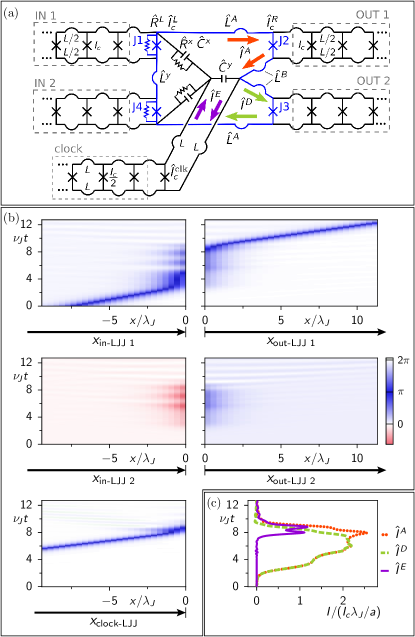
V A CNOT gate in RFL
Some of our 2-bit logic gates are purely ballistic, i.e. the logic action is generated alone through the inertia of (synchronous) input fluxons. Examples include the NSWAP [9] and IDSN gate. However, fluxon dynamics in the 2-bit gate circuit, Fig. 1(b), can only render a subset of all reversible 2-bit logic gates: namely those which act in the same way on an input state combination as on its inverse, e.g. on the input state (0,0) as on (1,1). Clearly, the NSWAP gate and IDSN gate (see table II) belong to this subset. The above restriction originates from the absence of an external magnetic field or stored flux, making the circuit dynamics invariant under a sign change of the phases. Additionally, a sign change of the input LJJ phases corresponds to the inversion of the input fluxon polarities, and thus to the inversion of the input bit states. Thus the gate dynamics resulting e.g. for the input state (0,0) is fully equivalent to that for input state (1,1).
Other reversible logic gates, such as the CNOT do not belong to the above-mentioned subset and thus cannot be achieved by a ballistic RFL gate alone. However, by combining ballistic logic gates with circuit elements for synchronization and routing we can construct more complex logic gates such as the CNOT [10]. Fig. 6(a) shows the schematic for an RFL implementation of a CNOT, which consists of two SNL clocking gates, two IDSN logic gates, and other routing components.
We shortly describe the operation of the composite CNOT: The input consists of two fluxons, carrying bit states A and B, respectively. Bit A comes in from the left on either of the input ports A1 or A2 of a 2-input SNL where it is stored. Similarly, bit B comes in on either B1 or B2 and is stored in a second SNL. Later a clock fluxon is sent in on a clock LJJ, which has regular LJJ characteristics . A T-branch splitter [25, 26] divides the original clock LJJ into two clock LJJs with characteristics , and as a result the original clock fluxon splits into two half-energy clock fluxons moving at the original speed. The two clock LJJs are each connected to a SNL, where the impinging clock fluxons synchronously launch the stored bit A and B as a fluxon or antifluxon. The launch is bit-state dependent, where the bit state 0 (1) is launched as a fluxon (antifluxon) into the upper (lower) output LJJ of each of the SNLs. We note that the two clock LJJs have to be wired to their respective SNL in a different way, in order to achieve the same launch directionality in both LJJs. This difference is indicated in Fig. 6 by the two distinct circuit symbols for the two SNLs. While the upper SNL corresponds exactly to the schematic of Fig. 5(a), the lower SNL has a half twist in the clock LJJ relative to that schematic.
The output LJJs of the two SNLs are connected to two IDSN gates in such a way that any bit state 0 of the two launched data fluxons will arrive at the upper IDSN and any bit state 1 will arrive at the lower IDSN. Depending on the initial bit states (A,B), either both IDSN gates receive a single fluxon as their input, or only one IDSN gate receives two input fluxons with the same polarity. According to the logic action of the IDSN, table II, in the former case the single input fluxon or antifluxon undergoes an ID operation. In the latter case, the two fluxons are well synchronized thanks to the simultaneous launch from the two SNLs. They will then both undergo NOT dynamics in the IDSN gate. The output fluxon(s) of the IDSN appear on its upper (lower) output LJJ if they entered on the upper (lower) input LJJ. Next, some of the fluxons pass through a NOT gate on the way to the output ports C1, C2, D1, D2 of the CNOT. The routing to these ports is done such that exactly one fluxon arrives on either C1 or C2, and thus uniquely defines the output bit C of the CNOT gate. Similarly, exactly one fluxon arrives on either D1 or D2 and defines the output bit D. The combined action of the clocking gates (SNL), ballistic logic gates (IDSN, NOT), and the routing ensures that these output bit states are related to the input bit states in form of the CNOT logic, see table in Fig. 6(b). These bits can then each be stored in another SNL for subsequent processing if desired. For example, one can cascade two CNOTs after one another to logically reverse the operation.
VI Conclusion
Reversible digital logic is important for the future development of computing because of the much higher energy efficiency compared with irreversible logic gates, including industry CMOS gates and the most developed SFQ logic. Recent demonstrations of such gates in superconducting circuits are adiabatic-reversible, making use of the inverse scaling between gate time and energy cost. In contrast, we are developing Reversible Fluxon Logic (RFL) based on ballistic-reversible gates. These are powered alone by the inertia of incoming fluxons which at the same time are the input bits themselves. The ballistic gates in RFL exploit a resonant scattering process at special interfaces between LJJs. This scattering achieves conditional polarity inversion of an input fluxon, dependent on the gate type and input bits. The advantage of RFL over irreversible logic is the full conservation of the rest (potential) energy of fluxons in logic operations. In our simulations this makes up of the fluxons’ total energy. Ballistic-reversible gates moreover conserve a large fraction of the kinetic fluxon energy, thus yielding conservation of up to of fluxon energy. Ballistic-reversible gates include the 1-bit NOT and ID, and the 2-bit NSWAP and IDSN gates.
The CNOT is implemented in RFL as a composite gate from a set of ballistic and non-ballistic gates. This includes two IDSN gates, three fundamental NOT gates, and two Store-and-Launch (SNL) gates. The SNL is a clocking gate that stores the bit state of an incoming fluxon and later launches it as a new fluxon on a bit-state dependent output LJJ. In the SNL version described here, the launch is powered by a clock fluxon at half of the data fluxon energy. In the CNOT, the data fluxon launch from the two SNL gates is synchronized, using the simultaneous arrival of clock fluxons which are fanned out from a single source.
Unlike the ballistic RFL gates which are nominally undamped the SNL gate uses damping resistors to ensure that the incoming data fluxon gets stored as a static flux in the SNL storage cell. In the launch process the clock fluxon is annihilated. A part of its energy goes to the launched data fluxon, which then may end up with larger energy than the input data fluxon. The other, larger part of the clock fluxon energy is dissipated in the resistors. However, since the clock fluxon has only a fraction of the data fluxon’s energy, and since much of the rest energy of the input data fluxon is preserved, the SNL gate may be very efficient by irreversible logic standards.
These studies indicate that reversible computing should not be thought of only in terms of the adiabatic model. Ballistic-reversible gates enabled by resonant fluxon scattering seem to be an implementable alternative. Combined with clocking gates that preserve the rest energy of the bits, ballistic gates can be used to build complex logic gates.
Acknowledgements
KDO would like to thank Quentin Herr, Mike Frank, Naoki Takeuchi, Nobuyuki Yoshikawa, Gary Delp and Ivan Sutherland for discussions on logic gates. KDO and WW would also like to acknowledge Liuqi Yu at LPS for scientific discussions on experimental designs of RFL. WW would like to thank the Physics department at the University of Otago for its hospitality.
[Modelling an LJJ with weakly excited edge state]
In the single-fluxon operation of the IDSN gate, where e.g. the fluxon comes in and leaves on LJJs and , the two other LJJs and are only weakly excited throughout the gate operation, cf. Fig. 3(b). The phase fields temporarily excited in these LJJs have the form of exponentially localized edge states at the interface and undergo a slow coherent oscillation. The contribution of each of those LJJs – including the parallel interface JJ – can then be analyzed in terms of a model, which parametrizes the phase fields as edge states, e.g. on the lower right interface JJ and LJJ ,
| (3) |
with an inverse decay length . Herein, labels the lower right interface JJ with characteristics , and label the JJs in in increasing distance from the interface.
For concreteness we show here how the model is applied to the right LJJ ; the same procedure applies to . The starting point for the analysis is the circuit Lagrangian of together with the lower right interface JJ,
| (4) |
For small amplitudes , Eq. (Acknowledgements) can be expanded to quadratic order in . We insert Eq. (3) and extend the sums, , under the assumption that the LJJ size is much larger than the decay length of the edge state, . With these approximations the Lagrangian reduces to that of a simple LC-oscillator of the edge phase ,
| (5) |
with -dependent effective parameters
| (6) | |||||
| (7) |
Herein we have defined the functions
| = | (e^2μa - 1)^-1 | (8) | |||||
| = | (e^μa - 1)^2 f(μ) | (9) |
Since we can also interpret Eq. (5) as the Lagrangian of a single JJ expanded to lowest orders. This JJ has (shunt) capacitance and critical current ,
| (10) |
By construction, the dynamics of this JJ should be equivalent to the dynamics of the lower right interface JJ together with the parallel LJJ , provided that it is only weakly excited by a fluxon from . We can apply the same model to the lower left interface JJ and LJJ , with edge state ansatz
| (11) |
where and label the JJs in the LJJ with increasing distance from the interface. Because of the left-right symmetry of the 2-bit gate structure, the resulting equivalent JJ of course has the same parameters, and .
In the edge state ansatz, Eqs. (3) and (11), the inverse decay length is still an unknown parameter and remains to be evaluated. Here we fix by the condition that the plasma frequency of the effective JJ matches the frequency, with which the edge state oscillates, . We approximate the latter as the oscillation frequency in the bulk of the LJJ, which follows from the bulk equations of motion,
| (12) |
After linearizing for small excitations, , and inserting Eq. (3) or Eq. (11) we obtain the bulk dispersion relation
| (13) |
In the homogeneous limit, , where Eq. (12) turns into the Sine-Gordon equation, , Eq. (13) simplifies to .
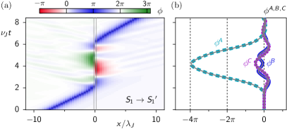
Fig. 7 shows from Eq. (13) (black dashed) together with the plasma frequency of the effective JJ (green solid). For the latter we have used the parameters of the IDSN interface, cf. the caption of Fig. 3. At the intersection point, , , both relations between frequency and inverse decay length are satisfied. The inset of Fig. 7 illustrates the edge states in LJJs and for this -value, and for . With and the parameters of the IDSN interface we obtain and . With these parameters the 1-bit structure shown in the right column of table III is approximately dynamically equivalent to the 2-bit IDSN structure under single-fluxon input, as demonstrated by Fig. 8, in comparison with Fig. 3(b).
References
- [1] C.H. Bennett, Logical Reversibility of Computation, IBM Journal of Research and Development 17, 525 (1973).
- [2] K.K. Likharev, Classical and quantum limitations on energy consumption in computation, Int. J. Theor. Phys. 21, 311 (1982).
- [3] N. Takeuchi, Y. Yamanashi, and N. Yoshikawa, Reversible logic gate using adiabatic superconducting devices, Sci. Rep. 4, 6354 (2014).
- [4] J. Ren and V.K. Semenov, Progress With Physically and Logically Reversible Superconducting Digital Circuits, IEEE Trans. Appl. Supercond. 21, 780 (2011).
- [5] E. Fredkin and T. Toffoli, Conservative Logic, Int. J. Theor. Phys. 21, 219 (1982).
- [6] C.E. Soccolich, M.W. Chbat, M.N. Islam and P.R. Prucnal, Cascade of ultrafast soliton-dragging and trapping logic gates, IEEE Photonics Technology Letters 4, 1043 (1992).
- [7] J. Scheuer and M. Orenstein, All-optical gates facilitated by soliton interactions in a multilayered Kerr medium, J. Opt. Soc. Am. B 22, 1260 (2005).
- [8] M.F. Ferreira, M.V. Facão, S.V. Latas, and M.H. Sousa, Optical Solitons in Fibers for Communication Systems, Fiber and Integrated Optics 24, 287 (2005).
- [9] W. Wustmann and K.D. Osborn, Reversible fluxon logic: Topological particles allow ballistic gates along one-dimensional paths, Phys. Rev. B 101, 0.14516 (2020).
- [10] K.D. Osborn and W. Wustmann, Ballistic reversible gates matched to bit storage: Plans for an efficient CNOT gate using fluxons, in Reversible Computation. RC 2018. Lecture Notes in Computer Science 11106, 189 (Springer, Cham, 2018).
- [11] M.P. Frank, Asynchronous ballistic reversible computing, 2017 IEEE International Conference on Rebooting Computing (ICRC), Washington, DC (2017).
- [12] M.P. Frank, R.M. Lewis, N.A. Missert, M.A. Wolak, and M.D. Henry, Asynchronous Ballistic Reversible Fluxon Logic IEEE Trans. Appl. Supercond. 29, 1302007 (2019).
- [13] M.P. Frank, R.M. Lewis, N.A. Missert, M.D. Henry, M.A. Wolak, and E.P. DeBenedictis, Semi-Automated Design of Functional Elements for a New Approach to Digital Superconducting Electronics: Methodology and Preliminary Results, 2019 IEEE International Superconductive Electronics Conference (ISEC), Riverside, CA, USA (2019).
- [14] H. Terai, Y. Kameda, S. Yorozu, A. Fujimaki, and Zhen Wang, The effects of DC bias current in large-scale SFQ circuits, IEEE Trans. Appl. Supercond. 13, 502 (2003).
- [15] J.H. Kang and S.B. Kaplan, Current recycling and SFQ signal transfer in large scale RSFQ circuits, IEEE Trans. Appl. Supercond. 13, 547 (2003).
- [16] M.H. Volkman, A. Sahu, C.J. Fourie, and O.A. Mukhanov, Implementation of energy efficient single flux quantum digital circuits with sub-aJ/bit operation, Supercond. Science and Technology 26, 015002 (2012).
- [17] L. Yu, W. Wustmann, and K.D. Osborn, Experimental designs of ballistic reversible logic gates using fluxons, 2019 IEEE International Superconductive Electronics Conference (ISEC), Riverside, CA, USA (2019).
- [18] R.H. Goodman and R. Haberman, Chaotic Scattering and the n-Bounce Resonance in Solitary-Wave Interactions, Phys. Rev. Lett. 98, 104103 (2007).
- [19] G. Costabile, R.D. Parmentier, B. Savo, D.W. McLaughlin, and A.C. Scott Exact solutions of the sine‐Gordon equation describing oscillations in a long (but finite) Josephson junction, Appl. Phys. Lett. 32, 587 (1978).
- [20] S. Ghoshal and A. Zamolodchikov, Boundary S-Matrix and Boundary State in Two-Dimensional Integrable Quantum Field Theory, Int. J. Mod. Phys. A 9, 3841 (1994).
- [21] Z. Fei, Y.S. Kivshar and L. Vázquez, Resonant kink-impurity interactions in the sine-Gordon model, Phys. Rev. A 45, 6019 (1992).
- [22] D.V. Averin, K. Rabenstein, and V.K. Semenov, Rapid ballistic readout for flux qubits, Phys. Rev. B 73, 094504 (2006).
- [23] M.P. Frank, Foundations of Generalized Reversible Computing, in Reversible Computation. RC 2017. Lecture Notes in Computer Science 10301, 19 (Springer, Cham, 2017).
- [24] M.P. Frank, Generalized Reversible Computing, arXiv:1806.10183 (2018).
- [25] K. Nakajima, Y. Onodera, and Y. Ogawa, Logic design of Josephson network, J. Appl. Phys. 47, 1620 (1976).
- [26] K. Nakajima, H. Sugahara, A. Fujimaki, and Y. Sawada, Experimental analysis of phase-mode Josephson digital circuits, J. Appl. Phys. 66, 949 (1989).
| Kevin D. Osborn received a B.S. in physics from Mary Washington University in Fredericksburg, Virginia and an M.S. with thesis in physics from the University of Tennessee, Knoxville in 1992 and 1995, respectively. He then matriculated to the Physics Department at the University of Illinois at Urbana-Champaign and completed his Ph.D. in 2001 with thesis studies of superfluid density fluctuations in high-temperature superconductors. Afterwards he transferred to the National Institute of Standards and Technology in Boulder, Colorado. Projects completed there included work on single-electron transistors over semiconductor quantum dots for quantum key distribution, and the development of superconducting qubits and coherent resonators. In 2007, Dr. Osborn started a research group in quantum computing at the Laboratory for Physical Sciences, with a joint appointment in the Physics Department, at the University of Maryland in College Park, MD. Most of Dr. Osborn’s over 40 publications are on qubits and two-level systems in materials, including custom quantum resonators to study them. In 2012, he hosted a workshop on reversible computing in Annapolis, MD, and since then he has kicked off research in that subfield of digital superconducting electronics. Dr. Osborn is the first-listed inventor on two recent patents in reversible digital computing. |
| W. Wustmann received diploma and Ph.D. degrees in theoretical physics at the Technical University in Dresden, Germany, in 2006 and 2010, respectively. Her graduate studies dealt with the statistical mechanics of periodically driven quantum systems. She then studied as a postdoc at Chalmers University in Gothenburg, Sweden, on the topic of parametric resonance in superconducting microwave circuits. Ever since this work she has contributed to and published with experimental groups. In 2014 she joined the Laboratory for Physical Sciences in College Park, to work on theory and simulation of flux soliton dynamics in long Josephson junction circuits. She is currently hosted by the University of Otago, New Zealand. |