Two-dimensional hole gas in organic semiconductors
Abstract
A highly conductive metallic gas that is quantum mechanically confined at a solid-state interface is an ideal platform to explore nontrivial electronic states that are otherwise inaccessible in bulk materials . Although two-dimensional electron gas (2DEG) has been realized in conventional semiconductor interfaces , examples of two-dimensional hole gas (2DHG), which is the counter analogue of 2DEG, are still limited . Here, we report the observation of a 2DHG in solution-processed organic semiconductors in conjunction with an electric double-layer using ionic liquids. A molecularly flat single crystal of high mobility organic semiconductors serves as a defect-free interface that facilitates two-dimensional confinement of high-density holes. Remarkably low sheet resistance of 6 k and high hole gas density of 1014 cm-2 result in a metal-insulator transition at ambient pressure. The measured degenerated holes in the organic semiconductors provide a broad opportunity to tailor low-dimensional electronic states using molecularly engineered heterointerfaces.
Material Innovation Research Center (MIRC) and Department of Advanced Materials Science, Graduate School of Frontier Sciences, The University of Tokyo, 5-1-5 Kashiwanoha, Kashiwa, Chiba 277-8561, Japan
AIST-UTokyo Advanced Operando-Measurement Technology Open Innovation laboratory (OPERAND-OIL), National Institute of Advanced Industrial Science and Technology (AIST), 5-1-5 Kashiwanoha, Kashiwa, Chiba 277-8561, Japan
International Center for Materials Nanoarchitectonics (WPI-MANA), National Institute for Materials Science (NIMS), 1-1 Namiki, Tsukuba, Ibaraki 305-0044, Japan
Precursory Research For Embryonic Science and Technology (PRESTO), Japan Science and Technology Agency (JST), Kawaguchi, Saitama 332-0012, Japan
A metallic gas confined in semiconductor heterostructures, which is also known as a two-dimensional electron gas (2DEG) or two-dimensional hole gas (2DHG), is one of the most intriguing platforms not only for exploring the fundamentals of condensed matter [1, 2] but also for developing high performance devices [3, 4]. Over the past four decades, the discovery of 2DEGs at the interface between compound semiconductors [5, 6] as well as at the interface between oxide insulators [7, 8] has provided an in-depth understandings of the nontrivial electronic states that are otherwise inaccessible in a bulk material [9]. Although 2DEGs with a remarkably high sheet conductivity at n-type interfaces have been discovered and are widely used in various high frequency devices (high-electron-mobility transistors are the most representative example), the use of its counter analogue, ., 2DHGs, at p-type interfaces, are still limited [10, 11]. The lack of these 2DHGs is rooted in the physics of conventional semiconductor heterointerfaces; wide-gap semiconductors generally lead to heavy valence bands, resulting in low mobility holes and deep valence bands [11]. In addition, extra attention should be paid to lattice continuity with respect to atomic scale precision, establishment of polar discontinuity, and extreme elimination of dangling bond, whose excess electrons often suppress hole transport [10].
Metallic phases under high carrier densities have been extensively studied in the field of organic semiconductors (OSCs) [12, 13, 14, 15, 16, 17, 18, 19, 20]. Recent studies have shown that self-assembled molecules without any dangling bonds can construct highly periodic electrostatic potential, and a coherent band hole system is realized, even in van der Waals bonded molecular crystals [21, 22, 23]. Despite the recent success in the field of materials science or in the developments in printing technologies for the single-crystalline forms of OSCs [24], an apparent metallic gas state has not been observed in OSCs. This is clearly because both static as well as dynamic disorders result in the carrier localization . large fluctuations in the intermolecular transfer integrals caused by thermal molecular motions are negligible even in the single crystals of OSCs.
Here, we demonstrate solution-processed, organic 2DHGs in which the metallic gas can be confined electrostatically within a monolayer of the OSCs. OSCs have been studied extensively as frontier materials for the development of new generation electronics. Recently, improvements in synthetic routes and device fabrication techniques have led to the development of small-molecule OSCs with high carrier mobility of 10 cm2 V-1 s-1 [25, 22, 26, 27, 28, 29]. We unambiguously demonstrate a metal-insulator transition (MIT) in the solution-processed, single-crystalline OSC at ambient pressure. In this, an extremely high carrier density of approximately 1 1014 cm-2 (approaching 0.25 holes per molecule) can be confined two-dimensionally at the OSC/electric double-layer (EDL) interface. An apparent metallic signature, the positive temperature coefficient of the resistance ( 0), is observed concomitantly with a minimum resistance of 6 k (below the two-dimensional quantum value , is the elementary charge and is the Planck constant) down to a temperature of = 15 K. This has not yet been demonstrated in a single component of OSCs. This observation is in striking contrast to the localized nature of the electronic states in OSCs and is manifested such that the degenerated electronic states are realized in OSCs.
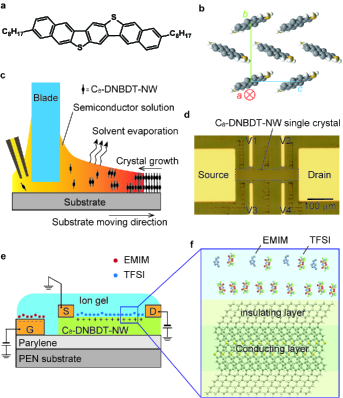
As an ideal organic two-dimensional system, we employ an alkyl-substituted small molecule. A truly single-crystalline form of 3,11-dioctyldinaphtho[2,3-d:2’,3’-d’]benzo[1,2-b:4,5-b’]dithiophene (C8-DNBDT-NW, Figs. 1a and b) is deposited on a flexible substrate via the continuous edge-casting method [30, 26, 28] (Fig. 1c). The continuous edge-casing method allows a one-shot crystal growth of layer-controlled thin films of C8-DNBDT-NW with an areal coverage of up to at least 1 cm2 [26, 28]. This is large enough to cover an entire channel (Fig. 1d). Technically, this one-shot printing method allows the fabrication of defect-free, single-crystalline nanosheets with large areal-coverage of up to 100 cm2 [28] onto any given substrate [31]. The single crystallinity across the C8-DNBDT-NW thin film has been confirmed by X-ray diffraction and electron diffraction measurements [29, 31]. A uniform optical intensity in polarized microscopy images confirms the existence of a molecularly flat surface without molecular steps. A single-crystalline bilayer is prepared selectively by controlling the substrate temperature [26, 32]. A plastic substrate (polyethylene naphtalate: PEN) coated with a parylene layer is a better alternative with regard to the thermal expansion coefficient of OSCs, less crystal cracks are induced during low temperature measurements. Gold/chromium electrodes are deposited gently on the surface of the bilayer C8-DNBDT-NW to form source and drain electrodes (a photograph of the device is shown in Fig. 1d). The channel direction is along the -axis of C8-DNBDT-NW . In this work, we use an ion gel as an electrolyte, in which the cations and anions of an ionic liquid (IL; 1-ethyl-3-methylimidazolium: [EMIM] and bis(trifluoromethylsulfonyl)imide: [TFSI], respectively) are enclosed by poly(vinylidene fluoride-co-hexafluopropylene)(P(VDF-HFP)) networks. An ion gel sheet comprising [EMIM][TFSI] is then placed onto the channel and pre-deposited gate electrode to form a side-gate configuration (Fig. 1e, details in Method section).
Previous studies have revealed that the EDL formed particularly at the surface of the OSC causes an unavoidable dissolution/damage [33]. In contrast, an insulating alkyl side chain of C8-DNBDT-NW with a thickness of 1 nm can separate the conducting layer of C8-DNBDT-NW from the IL (Fig. 1f). It is possible that the alkyl side chains provide indirect contact of the IL with the C8-DNBDT-NW molecules and suppress the electrical potential fluctuation, which is an origin of the carrier localization[34].
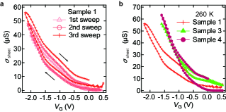
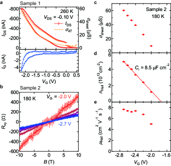
To assess the formation of the EDL at the surface of C8-DNBDT-NW , charging/discharging properties are investigated based on the standard EDLT characteristics. Figure 2a shows the transfer characteristics of sample 1 at a temperature of = 260 K upon application of drain voltage V. The drain current monotonically increases upon the application of negative gate voltage , showing a typical p-type operation. The gate current , which corresponds to the displacement current during charging/discharging, is found to be of the order of A and two orders of magnitude smaller than . This strongly suggests that charge carriers can be induced electrostatically rather than electrochemically. The formation of the EDL is further verified from the reproducible scans of . Four-terminal sheet conductivities as a function of ( are the lengths between the four-terminal voltage probes ( is the channel width, and is the potential difference between the four-terminal voltage probes) and are found to reach up to 60 (equivalently, the sheet resistance of 17 k, see Fig.2a for sample 1) at = 260 K and is at least five times larger than those attainable with conventional field effect transistor (FETs) with solid-state dielectrics [26]. Of the four samples examined in this work, the highest was achieved for sample 1, and detailed - and -variant was investigated for sample 2. We would emphasize that all the four samples show signs of metallic conduction and 2DHG behaviour at low temperatures (see the summary of sample variation in Extended data figure 1).
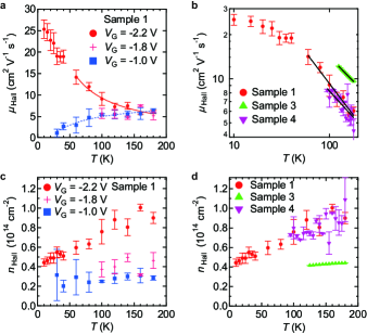
The Hall effect for each sample was measured with a helium gas-exchanged cryostat. Figure 2b shows the typical Hall resistance profile with respect to an external magnetic field for sample 2 at various at = 180 K. The positive slope of with respect to indicates that the charge carrier accumulated at the interface of C8-DNBDT-NW is hole, which is consistent with the p-type operation observed in the transfer characteristics. The sheet conductivity , Hall carrier density , and Hall mobility at with various , which are derived using the standard procedure of Hall effect measurements, are summarized in Figs. 2c–e. and increase linearly with increasing . Linear fitting of ()reveals that the capacitance of EDL between IL and C8-DNBDT-NW is is 8.5 F cm-2, which is consistent with the literature value [35]. These results lead to the conclusion that the carriers are induced electrostatically, the contribution of electrochemical doping is negligible. at =180 K increases from 5.0 cm2 V-1 s-1 at = 2.0 V to 7.7 cm2 V-1 s-1 at = 2.7 V (Fig. 2e), which is slightly smaller than those obtained for FETs with solid-state dielectrics [26]. The decrease in mobility for the two-dimensional electron systems has been often observed, particularly when a high electric field (normal to two-dimensional sheet) is applied [36]. It is possibly because not only ordinary phonon scattering but also other scattering such as scattering by ionized impurity may contribute to the carrier transport [10, 11, 2].
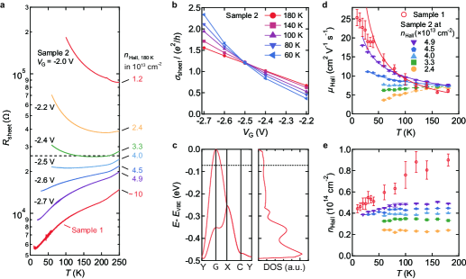
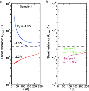
Temperature-dependence of sheet resistance -1 was investigated after the introduction of holes into the channel at = 260 K with various (Fig. 3a). At = 2.0 to 2.4 V, a typical semiconducting behaviour is observed, in which the temperature-dependence changes from metallic behaviour due to carrier transport dominated by phonon scattering above 200 K to insulating behaviour below 200 K. The increase in with indicates the gradual formation of degenerate holes, and enhanced mobility at low temperatures. Significantly, a positive temperature coefficient is observed when further holes are accumulated into the channel at = 2.6 and 2.7 V, where a metallic signature continues at the temperature of = 20 K. (= 2.7 V) is evaluated to be 20 k at 260 K and decreases to 9 k at 20 K for sample 2, and the minimum of 6 k is achieved for sample 1. The positive is observed reproducibly for the other samples (see Extended data figure 2). Such an apparent signature of metal-insulator transition has never been achieved for heterointerfaces of OSCs. It can be clearly attributed to the strong carrier localization, which could not be overcome for any of the existing OSCs. materials [12, 13, 14, 15, 16, 17, 18, 19, 20]. We emphasize that high-quality crystals even in the absence of surface crystal steps would be essential for the emergence of a 2DHG system at the heterointerfaces. Figure 3b shows the of sample 2 normalized by conductivity quantum as a function of . The temperature-independent crossing point can be seen at a well-defined = 2.5 V ( = 4 1013 cm-1, equivalently 0.1 holes per molecule), which clearly segregates the metallic and insulating phases [37]. The emergence of metallic ground state in highly doped C8-DNBDT-NW is also consistent with the Mott-Ioffe-Regel criterion ( = is the Fermi wave vector and = is the mean free path of the charge carriers) [38], suggesting that the two-dimensional hole gas can be realized at the interface between single-crystal C8-DNBDT-NW and IL.
The observation of metallic states in C8-DNBDT-NW EDLTs can be associated with the strongly correlated two-dimensional (2D) hole gas. As carriers induced by EDLT are confined in two dimension, the Coulomb interaction between holes result in a large , which is the ratio of the hole-hole interaction and Fermi energy :
where is the degenerate valley, is the effective mass of carriers, is the dielectric constant of the semiconductor, and is the carrier density. Generally, when is larger than 1, the Coulomb interaction is not negligible and causes two-dimensional metal-insulator transition (2D MIT). Given the , ( is the mass of free holes) as an average effective mass in -plane of C8-DNBDT-NW , typical dielectric constant of OSCs[39] and carrier density obtained in this work cm-2, we evaluate to be , which is comparable to those obtained for inorganic 2D systems (for example, 8 for Si metal-oxide-semiconductor FETs[40], 5 for GaAs/AlGaAs heterostructure[41], and 4 for monolayer MoS2 [42].). This implies that highly doped C8-DNBDT-NW can be classified into the strongly correlated 2D system. The strong Coulomb interaction is further evidenced by the determination of Fermi energy. According to a previous report [43], the trap density of C8-DNBDT-NW single crystal is sufficiently low, , the pinning of the Fermi energy in the band gap is negligibly small, so that the Fermi energy can be shifted effectively as the carrier density varies. Given typical values of 4 1013 cm-2, the Fermi energy is shifted by 71.8 meV below the top of the valence band at = 260 K, leading to the Fermi degeneracy of C8-DNBDT-NW (Fig. 3c).
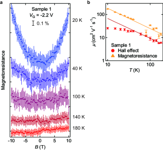
Figures 3d and e display the -dependence of and at various of samples 1 and 2 (see Extended data figure 3 for the other samples). measured below 4.0 1013 cm-2 decreases as decreases, indicating that holes below the critical point undergo multiple-trapping-and-release conduction between the valence band and shallow trap states (within a few regions from the top of the valence band) [21]. We determine the activation energy = 2.2 meV at = 2.4 1013 cm-2 and 0.58 meV at = 3.3 1013 cm-2 by fitting temperature-variant with the Arrhenius-type thermally activated model exp, which is small enough to activate from shallow trap states to valence band and is consistent with the weak temperature dependence of Hall carrier density at low temperatures (Fig. 3b). In contrast, measured above 4.0 1013 cm-2 increases monotonically as decreases (Fig. 3b), where is estimated to be 7 cm2 V-1 s-1 at 180 K, and increases up to 26 cm2 V-1 s-1 at 10 K. The temperature-dependence of can be fitted with the power law behaviour . The exponent in the power-dependence is estimated to be = 0.24 at 4.5 1013 cm-2, = 0.46 at 4.9 1013 cm-2, and = 0.86 at 10 1013 cm-2. This is in good agreement with the exponent values of dominated by phonon scattering, which has been observed experimentally and theoretically for C8-DNBDT-NW [22]. Although the high exceeding 20 cm2 V-1 s-1 is reproducibly observed, a discrepancy in the temperature-dependence of from the power-law behaviour is found below = 50 K. This behaviour is consistent with typical 2D electron/hole systems, in which carrier transport is dominated by phonon scattering at elevated temperatures. Consequently, it is dominated by the scattering of defect impurities at cryogenic temperatures, resulting in suppressed mobility [2]. In addition, the observation of positive longitudinal mangetoresistance is consistent with that expected in degenerated electron/hole systems. (see Extended data figure 4).
is estimated to be 1 1014 cm-2 at 200 K and 4 1013 cm-2 at 15 K. Remarkably high carrier density approaching 1 1014 cm-2 at room temperature corresponds to 0.25 holes per molecule, which is the highest carrier density observed in OSCs to the best of our knowledge, and clearly shifts the Fermi energy below the top of the valence band, leading the Fermi degeneracy. The decrease in as temperature decreases does not imply a decrease in the actual carrier density because EDL can electrostatically confine the net of holes at the interface. In fact, this trend has been often observed for many of 2D electron/hole gasses and is interpreted as the crossover in different carrier scattering mechanism, most likely the cross over from phonon scattering at higher temperature to ionized impurity scattering at lower temperatures. This interpretation does not contradict to the mobility saturation at lower temperatures (Fig. 3d). Alternatively, it is envisaged that the strong hole-hole interaction may induce a soft gap at the Fermi energy, resulting in a reduction of density-of-states. Although further researches will be necessary to fully understand electronic properties in 2DHG in OSCs interface, the presence of degenerated hole systems concomitantly with the signature of metal-insulator transition has been demonstrated for the first time in the OSC heterointerface.
This study unambiguously demonstrates a metal–insulator transition in OSCs at ambient pressure for the first time. The metallic gas state with high a carrier density of 0.25 holes per molecule and remarkably low sheet resistance of 6 k is experimentally observed. In a striking contrast with the localized nature of electronic states in OSCs, the observation of 2DHGs manifests itself, such that the static disorder inevitably found in OSCs is overcome. One-shot printing of semiconductor ink at room temperature allows for the ideal production of self-assembled, two-dimensional molecular nanosheets with a large areal coverage, up to 100 cm2. The technique employed in this study to achieve remarkably high carrier density can act as framework for the exploration of electronic phase transitions in strongly correlated electronic systems in OSCs.
Methods
Sample preparation
The electric double-layer transistors (EDLTs) studied in this work were fabricated on a polyethylene naphthalate (PEN) substrate. The PEN film (Teijin Ltd., Q65HA, 125 m) was pre-baked at 150 ∘C for 3 h to reduce internal stress and cooled down slowly to room temperature. After cleaning the PEN film with acetone and 2-propanol in an ultrasonic bath, parylene (dix-SR, KISCO Ltd.) was coated onto the PEN film via chemical vapor deposition, achieving a thickness of 200 nm. The single-crystal bilayer C8-DNBDT-NW was grown on the parylene layer from 3-chlorothiophene with a concentration of 0.020 wt% at 70 ∘C via the continuous edge casting method [30]. Gold (62 nm)/chromium (8 nm) were evaporated on the parylene/PEN substrate and single-crystal C8-DNBDT-NW through shadow masks to form the source, drain, side gate electrodes, and voltage probes. Laser etching (V-Technology Co., Ltd., Callisto (266 nm)) was carried out for the C8-DNBDT-NW layer to form Hall bar.
The ion gel film was spin-coated onto the PEN film (Teijin Ltd., Q51, 25 m) with a solution composed of poly(vinylidene fluoride-co-hexafluopropylene)(P(VDF-HFP)), ionic liquid (1-Ethyl-3-methylimidazolium: [EMIM] and bis(trifluoromethylsulfonyl)imide: [TFSI], respectively) and, acetonitrile (1:2:10 wt. ratio). After cutting the ion gel with the PEN film, EDLTs were completed by the lamination of the ion gel and the PEN film onto the Hall bar-shaped single-crystal C8-DNBDT-NW and side-top gate.
Transport measurement
Low-temperature magnetotransport measurements were performed at least 12 h after the EDLT sample was inserted into a He gas-exchange cryostat with a superconducting magnet. Transfer characteristics in the linear regime (at drain voltage V) were continuously recorded by a sweeping gate voltage at a rate of mV per s. Introduction of the holes onto C8-DNBDT-NW at 260 K was undertaken by applying , for which was negatively increased from V to the target voltage at a rate of mV per s. When was changed, samples were heated up to 260 K and discharged with V. After charging the C8-DNBDT-NW by applying the target at 260 K, the temperature dependence of the sheet resistance is measured by monitoring the drain current and the voltage probes. Constant V is applied during the slow ramping of downwards and upwards with the ramping rate of K min-1. Hall measurements were performed with a constant DC (A. During sweeping, an external magnetic field was applied perpendicular to the sample plane, not exceeding T and with a slow sweeping rate of 0.01 T s-1.
Determination of Fermi level
The observation of metallic states in single-crystal C8-DNBDT-NW with a high carrier density exceeding cm-2 in this work is accompanied by Fermi degeneracy. To investigate the relationship between the carrier density and Fermi level , we estimate the Fermi level of C8-DNBDT-NW from the following equation:
| (1) |
Where is the density of states of C8-DNBDT-NW and is the Fermi distribution function . The carrier density is estimated from the Hall effect at 180 K, and is assumed to be temperature-independent at least within the temperature from 180 K to 260 K. The density of states of C8-DNBDT-NW is calculated using CRYSTAL 17 at the B3LYP functional and POB-DZVP basis set level.
Acknowledgements
S.W. acknowledges the support from the Leading Initiative for Excellent Young Researchers of JSPS. T.O. acknowledges the support from PRESTO-JST through the project ”Scientific Innovation for Energy Harvesting Technology” (Grant No. JPMJPR17R2). This work was supported by Kakenhi Grants-in-Aid (Nos. JP17H06123, JP17H06200, 20H00387) from JSPS.
Author contributions
N.K. conceived, designed, and performed the experiments and analysed the data. N.K. and J. Tsurumi performed the DFT calculations. T.O. synthesized and purified C8-DNBDT-NW. N.K., S.W. and J. Takeya wrote the manuscript. S.W. and J. Takeya supervised the work. All authors discussed the results and reviewed the manuscript.
Competing financial interests
The authors declare no competing interests.
Data availability
The data that support the plots within this paper and the other findings of this study are available from the corresponding author (Shun Watanabe; swatanabe@edu.k.u-tokyo.ac.jp) upon request.
0.1 Reference
References
- [1] Ando, T., Fowler, A. B. & Stern, F. Electronic properties of two-dimensional systems. Reviews of Modern Physics 54, 437 (1982).
- [2] Davies, J. H. The Physics of Low-Dimensional Semiconductors, 290–366 (Cambridge University Press, New York, NY, USA, 1998).
- [3] Mimura, T. The early history of the high electron mobility transistor (hemt). IEEE Transactions on microwave theory and techniques 50, 780–782 (2002).
- [4] Pengelly, R. S., Wood, S. M., Milligan, J. W., Sheppard, S. T. & Pribble, W. L. A review of gan on sic high electron-mobility power transistors and mmics. IEEE Transactions on Microwave Theory and Techniques 60, 1764–1783 (2012).
- [5] Mimura, T., Hiyamizu, S., Fujii, T. & Nanbu, K. A new field-effect transistor with selectively doped gaas/n-alxga1-xas heterojunctions. Japanese Journal of Applied Physics 19, L225 (1980).
- [6] Ambacher, O. et al. Two-dimensional electron gases induced by spontaneous and piezoelectric polarization charges in n-and ga-face algan/gan heterostructures. Journal of Applied Physics 85, 3222–3233 (1999).
- [7] Ohtomo, A. & Hwang, H. A high-mobility electron gas at the laalo 3/srtio 3 heterointerface. Nature 427, 423–426 (2004).
- [8] Thiel, S., Hammerl, G., Schmehl, A., Schneider, C. W. & Mannhart, J. Tunable quasi-two-dimensional electron gases in oxide heterostructures. Science 313, 1942–1945 (2006).
- [9] Hwang, H. Y. et al. Emergent phenomena at oxide interfaces. Nature Materials 11, 103–113 (2012).
- [10] Lee, H. et al. Direct observation of a two-dimensional hole gas at oxide interfaces. Nature Materials 17, 231–236 (2018).
- [11] Chaudhuri, R. et al. A polarization-induced 2d hole gas in undoped gallium nitride quantum wells. Science 365, 1454–1457 (2019).
- [12] Chwang, A. B. & Frisbie, C. D. Temperature and gate voltage dependent transport across a single organic semiconductor grain boundary. Journal of Applied Physics 90, 1342–1349 (2001).
- [13] Takeya, J., Tsukagoshi, K., Aoyagi, Y., Takenobu, T. & Iwasa, Y. Hall effect of quasi-hole gas in organic single-crystal transistors. Japanese journal of applied physics 44, L1393 (2005).
- [14] Podzorov, V., Menard, E., Rogers, J. & Gershenson, M. Hall effect in the accumulation layers on the surface of organic semiconductors. Physical Review Letters 95, 226601 (2005).
- [15] Hulea, I. N. et al. Tunable fröhlich polarons in organic single-crystal transistors. Nature Materials 5, 982–986 (2006).
- [16] Takeya, J. et al. In-crystal and surface charge transport of electric-field-induced carriers in organic single-crystal semiconductors. Physical review letters 98, 196804 (2007).
- [17] Alves, H., Molinari, A. S., Xie, H. & Morpurgo, A. F. Metallic conduction at organic charge-transfer interfaces. Nature Materials 7, 574–580 (2008).
- [18] Xia, Y., Xie, W., Ruden, P. P. & Frisbie, C. D. Carrier localization on surfaces of organic semiconductors gated with electrolytes. Physical Review Letters 105, 036802 (2010).
- [19] Wang, S., Ha, M., Manno, M., Frisbie, C. D. & Leighton, C. Hopping transport and the hall effect near the insulator–metal transition in electrochemically gated poly (3-hexylthiophene) transistors. Nature Communications 3, 1–7 (2012).
- [20] Sakanoue, T. & Sirringhaus, H. Band-like temperature dependence of mobility in a solution-processed organic semiconductor. Nature Materials 9, 736–740 (2010).
- [21] Hasegawa, T. & Takeya, J. Organic field-effect transistors using single crystals. Science and Technology of Advanced Materials 10, 024314 (2009).
- [22] Tsurumi, J. et al. Coexistence of ultra-long spin relaxation time and coherent charge transport in organic single-crystal semiconductors. Nature Physics 13, 994–998 (2017).
- [23] Fratini, S., Ciuchi, S., Mayou, D., De Laissardière, G. T. & Troisi, A. A map of high-mobility molecular semiconductors. Nature Materials 16, 998–1002 (2017).
- [24] Fratini, S., Nikolka, M., Salleo, A., Schweicher, G. & Sirringhaus, H. Charge transport in high-mobility conjugated polymers and molecular semiconductors. Nature Materials 19, 491 (2020).
- [25] Mitsui, C. et al. High-performance solution-processable n-shaped organic semiconducting materials with stabilized crystal phase. Advanced Materials 26, 4546–4551 (2014).
- [26] Yamamura, A. et al. Wafer-scale, layer-controlled organic single crystals for high-speed circuit operation. Science Advances 4, eaao5758 (2018).
- [27] Okamoto, T. et al. Bent-shaped p-type small-molecule organic semiconductors: A molecular design strategy for next-generation practical applications. Journal of the American Chemical Society 142, 9083–9096 (2020).
- [28] Kumagai, S. et al. Scalable fabrication of organic single-crystalline wafers for reproducible TFT arrays. Scientific Reports 9, 15897 (2019).
- [29] Yamamura, A. et al. High-speed organic single-crystal transistor responding to very high frequency band. Advanced Functional Materials 30, 1909501 (2020).
- [30] Soeda, J. et al. Inch-size solution-processed single-crystalline films of high-mobility organic semiconductors. Applied Physics Express 6, 076503 (2013).
- [31] Makita, T. et al. High-performance, semiconducting membrane composed of ultrathin, single-crystal organic semiconductors. Proceedings of the National Academy of Sciences 117, 80–85 (2020).
- [32] Yamamura, A. et al. Sub-molecular structural relaxation at a physisorbed interface with monolayer organic single-crystal semiconductors. Communications Physics 3, 1–8 (2020).
- [33] Yokota, Y. et al. Structural investigation of ionic liquid/rubrene single crystal interfaces by using frequency-modulation atomic force microscopy. Chemical Communications 49, 10596 (2013).
- [34] Ovchinnikov, D., Gargiulo, F. & Allain, A. Disorder engineering and conductivity dome in res2 with electrolyte gating. Nature Communications 7, 12391 (2016).
- [35] Keun Hyung Lee, S. Z. Y. G. T. P. L., Moon Sung Kang & Frisbie, C. D. ”cut and stick” rubbery ion gels as high capacitance gate dielectrics. Advanced Materials 24, 4457–4462 (2012).
- [36] Takagi, S., Toriumi, A., Iwase, M. & Tango, H. On the universality of inversion layer mobility in si mosfet’s: Part i-effects of substrate impurity concentration. IEEE Transactions on Electron Devices 41, 2357–2362 (1994).
- [37] Sato, Y., Kawasugi, Y., Suda, M., Yamamoto, H., M & Kato, R. Critical behavior in doping-driven metal-insulator transition on single-crystalline organic mott-fet. Nano letters 17, 708–714 (2016).
- [38] Das Sarma, S. & Hwang, E. H. Two-dimensional metal-insulator transition as a strong localization induced crossover phenomenon. Physical Review B 89, 235423 (2014).
- [39] Haitao, S. et al. Ionization energies, electron affinities, and polarization energies of organic molecular crystals: Quantitative estimations from a polarizable continuum model (pcm)-tuned range-separated density functional approach. Journal of Chemical Theory and Computation 12, 2906–2916 (2016).
- [40] Okamoto, T., Hosoya, K., Kawaji, S. & Yagi, A. Spin degree of freedom in a two-dimensional electron liquid. Phys. Rev. Lett. 82, 3875–3878 (1999).
- [41] A., G. et al. Electron assisted variable range hopping in strongly correlated 2d electron systems. Physics State Solid (b) 230, 211–216 (2002).
- [42] Branimir, R. & Andras, K. Mobility engineering and a metal-insulator transition in monolayer mos2. Nature Materials 12, 815–820 (2013).
- [43] Watanabe, S. et al. Remarkably low flicker noise in solution-processed organic single crystal transistors. Communications Physics 1, 37 (2018).