Development of next-generation timing system for the Japan Proton Accelerator Research Complex
Abstract
A precise and stable timing system is necessary for high intensity proton accelerators such as the J-PARC. The original timing system, which was developed during the construction period of the J-PARC, has been working without major issues since 2006. After a decade of operation, the optical modules, which are key components for signal transfer, were discontinued already. Thus, the next-generation timing system for the J-PARC has been developed and built. The new system is designed to be compatible with the original system in terms of the operating principle. The new system utilizes modern high speed serial communication for the transfer of the clock, reference trigger, and type code. We describe the system configuration of the next-generation timing system and current status.
Index Terms:
Proton Synchrotron, Timing SystemI Introduction
The Japan Proton Accelerator Research Complex (J-PARC) [1] is a high intensity proton accelerator facility, which includes three accelerators, the 400 MeV linac, the 3 GeV rapid cycling synchrotron (RCS), and the 30 GeV main ring synchrotron (MR). The design output beam power of the RCS and MR is 1 MW and 750 kW, respectively. The RCS delivers high intensity proton beams to the Material and Life Science Experimental Facility (MLF) for generation of neutrons and muons and to the MR. The MR beams are delivered to the neutrino experiment and the hadron hall by fast extraction (FX) and slow extraction (SX) schemes, respectively. The beam commissioning of the J-PARC accelerators started in 2006. The beam intensity has been increased steadily with progress of the beam tuning and hardware upgrades. As of June 2020, the RCS output beam power for the MLF user program is 600 kW, and the MR beam power reached 510 kW and 51 kW for the neutrino experiment and the hadron experiments, respectively.
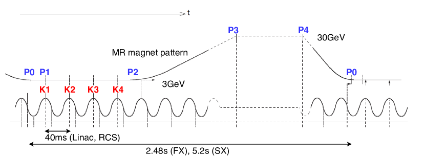
The operating cycle of the J-PARC accelerators is illustrated in Fig. 1. The linac and RCS are operated at the repetition rate of 25 Hz. The MR cycle, i.e., the whole operating cycle of the J-PARC, is 2.48 s and 5.2 s for the FX and SX modes, respectively. The MR cycle must be an integer multiple of the RCS period, 40 ms. Four RCS beam is injected to the MR at the K1 to K4 timing and the other beam is delivered to the MLF. The beam parameters of the linac and RCS, such as the macro pulse width, the chopping width, and the exciting pattern of the injection bump magnets, are different for the beam to the MLF and MR. Therefore, different timing signals for the devices of the linac and RCS are required during the MR cycle.
For high intensity proton accelerators such as the J-PARC, the beam loss reduction is important to avoid the residual activation of the components. A precise and stable timing system, which generates the triggers and gates for the accelerator devices, is necessary to realize the precise beam control for minimizing the beam losses. Typically, the jitter of the triggers must be less than 1 ns in the J-PARC.
At the J-PARC, two kinds of timing are defined; the scheduled timing and the synchronization timing. The scheduled timing is defined by the programmed delay from the 25 Hz reference trigger sent from the central control building (CCB). The synchronization timing is the timing signals generated by the accelerator devices to synchronize the beams. The linac chopper gate pulses are generated by the low level rf (LLRF) control system of the RCS so that the injected intermediate beam pulses into the RCS are centered to the rf buckets of the RCS. The trigger for the extraction kicker of the RCS and the injection kicker of the MR is also generated by the RCS LLRF control system. Most of the accelerator devices in the J-PARC are operated by the scheduled timing. We focus on the scheduled timing in this article.
The original timing system [2, 3] was developed during the construction period of the J-PARC. The system has been working without major problems since the start of the beam operation in 2006. However, the optical modules, which are key components in the timing system for signal transfer, have been discontinued already. We decided to develop the next-generation timing system in 2016 and the new modules were successfully deployed in 2020.
In this article, we describe the operating principle of the schedule timing and the configuration of the original timing system. The configuration of the next-generation timing system is presented. Also, the test results and the current status are described.
II Original timing system
II-A Operating principle of the scheduled timing
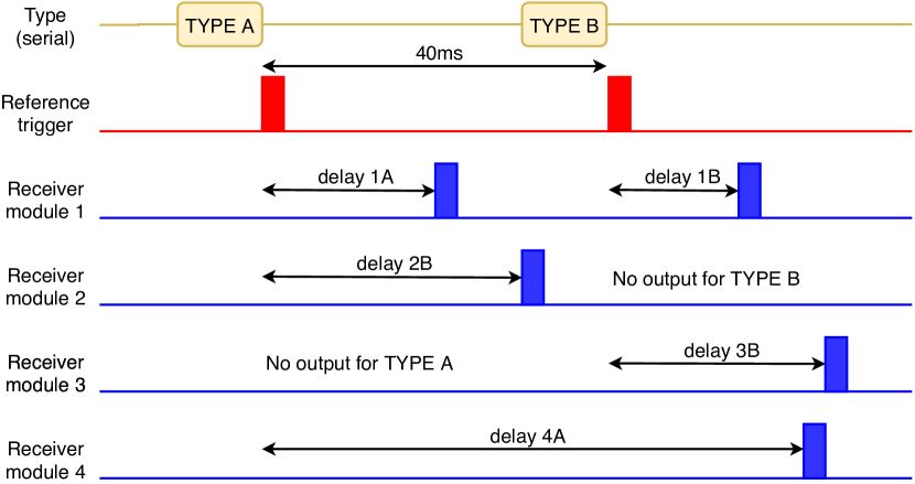
Operating principle of the scheduled timing is shown in Fig. 2. The 25 Hz reference trigger and the type code, which corresponds to the operation type of the accelerators for the next linac and RCS cycle, are sent from the CCB to the receiver modules in three accelerators and three experimental buildings. The type code is sent prior to the 25 Hz reference trigger.
The timing receiver module has a look-up table (LUT) with the type code as address. The behavior of the receiver after the next reference trigger is defined by the control word from the LUT. Three behaviors are defined as follows. First, the receiver outputs a trigger with the programmed delay. In the figure, the receiver module 1 and 2 output triggers at the delay 1A and 2A for TYPE A, respectively. For TYPE B, the module 1 and 3 generate the triggers the similar manner. Second, the output can be suppressed for the next 40 ms. The outputs of the receiver modules 2 and 3 are suppressed for TYPE B and A, respectively.
The delay value can be set longer than the 40 ms, as the delay 4A of the receiver module 4 for TYPE A in the figure, while normally the delay counter is reset with the next recerence trigger. With the special control word for TYPE B, the delay counter continues beyond the next reference trigger.
The type sequence, of which length is same as the MR cycle, represents the operation of the accelerators every 40 ms. If the end code is picked up from the type memory, the sequence start from the beginning of the type memory. In the case of the jump code, the next sequence starts with different type memory indicated by the jump code. When the type memory is switched manually by a software, the switching happens at the end or jump code. This guarantees the MR cycle is fixed during a run. By switching of the type sequence as well as the modification of the LUTs, various operation of the J-PARC accelerator is realized.
The operating principle is similar to the modern event timing system such as the MRF (Micro Research Finland) timing system [4], while the event, i.e., the type code, is sent in a fixed repetition of 25 Hz in the J-PARC timing system.
II-B Hardware configuration
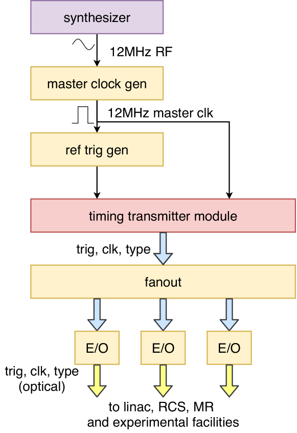
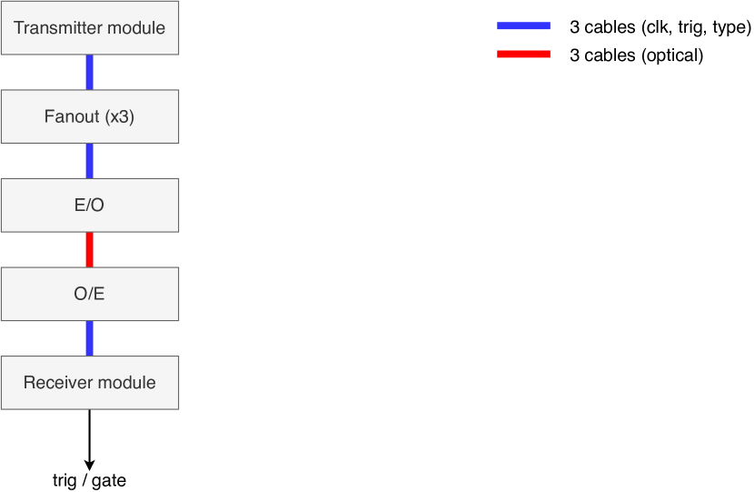
Figure 3 shows the signal flow of the timing transmitter station in the CCB. The 12 MHz master clock is generated by the master clock generator referring the rf signal from a high precision synthesizer. By counting the master clock, the 25 Hz reference trigger is generated. The timing transmitter module, which is the core of the J-PARC scheduled timing, outputs the serialized type code according to the programmed type sequence. Through the fanout module and the E/O (electrical/optical) converter, the three optical signals, the 25 Hz reference trigger, the master clock, and the type code, are sent to the facilities of the J-PARC.
The signal flow is a star configuration. All receiver modules in the facilities receive the same three signals. If necessary, a combination of the O/E, fanout, and E/O can be used to redistribute the signals at each facility.
The type code is a 32 bit word, with the first bit representing special information. Eight bits each are allocated to the linac, RCS, and MR. The remaining seven bits are reserved.
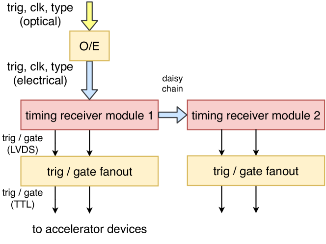
The signal flow of the timing receiver station is illustrated in Fig. 4. The optical signals of the 25 Hz reference trigger, the master clock, and the type code are converted by the O/E module to the electric signals and they are lead to the timing receiver module. The signals can be forwarded to another receiver modules with a daisy chain.
A 96 MHz clock is generated by a phase lock loop (PLL) in the receiver module referring the 12 MHz master clock. The delay counter in the module uses the 96 MHz clock. The receiver module retrieves the control word from the LUT by taking the specified 8 bits from the 32 bit type code. The behavior of the receiver module for the next 25 Hz reference trigger is defined by the control word, as described in the previous subsection. The delay value is 24 bit, therefore the delay counter can count up to 174 ms. The signal level of the receiver module is LVDS, and the following trigger and gate fanout module converts to the signal level for the accelerator devices.
The timing transmitter and receiver modules are VME modules, and the other modules are NIM module. In the linac and RCS, the reflective memory (RM) networks are configured together with the timing system [5]. The RM network enables fast rewriting the LUTs and sharing the beam tag information. A synchronized data acquisition at 25 Hz is realized with the RM network for the RCS and the fast data acquisition is indispensable for the commissioning and operation of the RCS [6].
We note here that the timing of the J-PARC is based on the 12 MHz master clock generated referring the high precision synthesizer, i.e., the accelerator cycle is not synchronized to the AC power line, which has a frequency variation in the order of 0.1%. The jitter of the generated triggers is very low, less than 1 ns. By the accurate timing system and the digital LLRF control system of the RCS, the very low beam timing jitter of 1.7 ns, which satisfies the requirement of the fermi chopper spectrometer [7] in the MLF, is achieved [8, 9].
II-C Demand of the next-generation timing system
The original timing system started its operation in 2006. Since then, the system has been working well without major problems for more than ten years. However, the optical device (Finisar v23826) in the E/O and O/E modules, which are the key modules for the signal transfer, has already been discontinued, and there are no successor devices. While we have an amount of spare modules, it will be soon difficult to maintain the original timing system. Therefore, we started to consider a next-generation timing system in 2016.
The number of the timing receiver modules is in the order of 200 [10]. It is not realistic to replace all of the original modules with the next-generation system at the same time. Therefore, the new system is designed to be compatible with the original system and the operating principle is employed as is. From this viewpoint, the popular timing solutions such as the MRF timing system [4] or the White Rabbit [11] are not considered to be employed.
After a decade of the operation, we found the following issues. It has been an infrastructure burden that the original system requires three optical or metal cables for transfer of three signals, the 25 Hz reference trigger, the master clock, and the type code, as shown in Fig. 5LABEL:sub@fig:timing_before. Also, the metal cable between the O/E module and the receiver module may pick up noises from the pulsed power supplies or the high intensity beams, even with short metal cables. The receiver module may suffer from the noises; We have experienced several hang-ups of the receiver module due to the noises.
A set of VME and NIM crates are necessary, which require an amount of space and cost, for the timing receiver station of the original system. This is an important issue especially for the MR, where the hardware extension is still ongoing and the new deployment of the receiver station is often required.
The next-generation system has been designed considering these issues.
III Next-generation timing system
| 1 | 2 | 3 | 4 | 5 | 6 | 7 | 8 | 9 | 10 | 11 | 12 | |
| seq | K28.5 | E | D(p1) | D(p2) | D(p3) | D(p4) | D(p5) | D(p6) | D(p7) | D(p8) | D(p9) | D(p10) |
| 1 | 2 | 3 | 4 | 5 | 6 | 7 | 8 | 9 | 10 | 11 | 12 | |
| Null | K28.5 | E(null) | D0.0 | D0.0 | D0.0 | D0.0 | D0.0 | D0.0 | D0.0 | D0.0 | D0.0 | D0.0 |
| 1 | 2 | 3 | 4 | 5 | 6 | 7 | 8 | 9 | 10 | 11 | 12 | |
| Trig | K28.5 | E(trig) | D0.0 | D0.0 | D0.0 | D0.0 | D0.0 | D0.0 | D0.0 | D0.0 | D0.0 | D0.0 |
| 1 | 2 | 3 | 4 | 5 | 6 | 7 | 8 | 9 | 10 | 11 | 12 | |
| Type | K28.5 | E(type) | type1 | type2 | type3 | type4 | D0.0 | D0.0 | D0.0 | D0.0 | D0.0 | D0.0 |
| 1 | 2 | 3 | 4 | 5 | 6 | 7 | 8 | 9 | 10 | 11 | 12 | |
| S | K28.5 | E(S) | D0.0 | D0.0 | D0.0 | D0.0 | D0.0 | D0.0 | D0.0 | D0.0 | D0.0 | D0.0 |
| 1 | 2 | 3 | 4 | 5 | 6 | 7 | 8 | 9 | 10 | 11 | 12 | |
| Scnt | K28.5 | E(Scnt) | Scnt1 | Scnt2 | Scnt3 | Scnt4 | D0.0 | D0.0 | D0.0 | D0.0 | D0.0 | D0.0 |
| 1 | 2 | 3 | 4 | 5 | 6 | 7 | 8 | 9 | 10 | 11 | 12 | |
| Tcnt | K28.5 | E(Tcnt) | Tcnt1 | Tcnt2 | Tcnt3 | Tcnt4 | D0.0 | D0.0 | D0.0 | D0.0 | D0.0 | D0.0 |
III-A System configuration
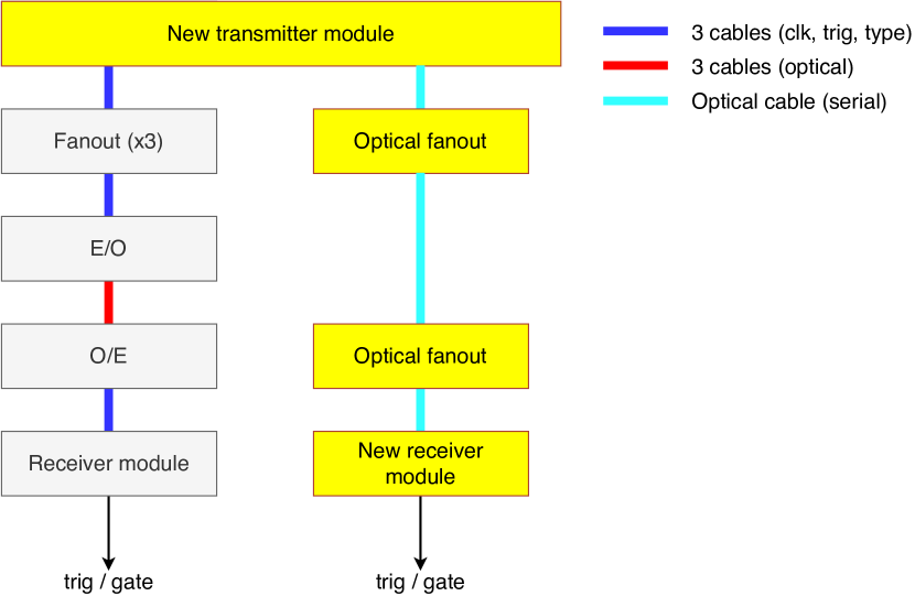
The configurations of the next-generation timing system is shown in Fig. 5LABEL:sub@fig:timing_after. In the figure, the blocks with yellow color are the newly developed modules.
The new timing transmitter module output a serialized optical signal, which contains the information of the 25 Hz reference trigger, 12 MHz clock, and the type code. The new transmitter also outputs the same three electrical signals as the original system, so that the existing signal distribution networks and the timing receiver stations as they are. This allows for a gradual transition to the next-generation system, while coexisting with the original timing modules.
A SFP (small form factor pluggable) optical transceiver, which is widely used today, is employed as the optical component for high speed serial communication. The optical signal from the new transmitter module is distributed to the new receiver modules in the facilities via the newly developed optical fanouts. Contrary to the original system, the optical signal is directly input to the new receiver module. It is expected that the malfunctions caused by the noises will be mitigated. Similar to the original receiver module, the optical signal can be forwarded to the another module forming a daisy chain.
The new receiver module decodes and extracts the 12 MHz clock, 25 Hz recerence trigger and type code from the received serial signal. After decoding the three signals, the operation is identical to that of the original receiver module.
The new transmitter and receiver modules are implemented as VME modules. The arrangement of the VME registers is the same as the existing module as much as possible, so that the development of the driver software is simple. The PLC type receiver module is also developed. The PLC receiver module is designed to output the triggers and gates at the required voltage level form the accelerator devices without the NIM modules. The PLC module is planned to be used extensively in the MR, which has many restrictions on the arrangement of the control devices.
III-B High speed serial communication
The configuration of the high speed serial communication in the next-generation timing system is shown in Fig. 6.
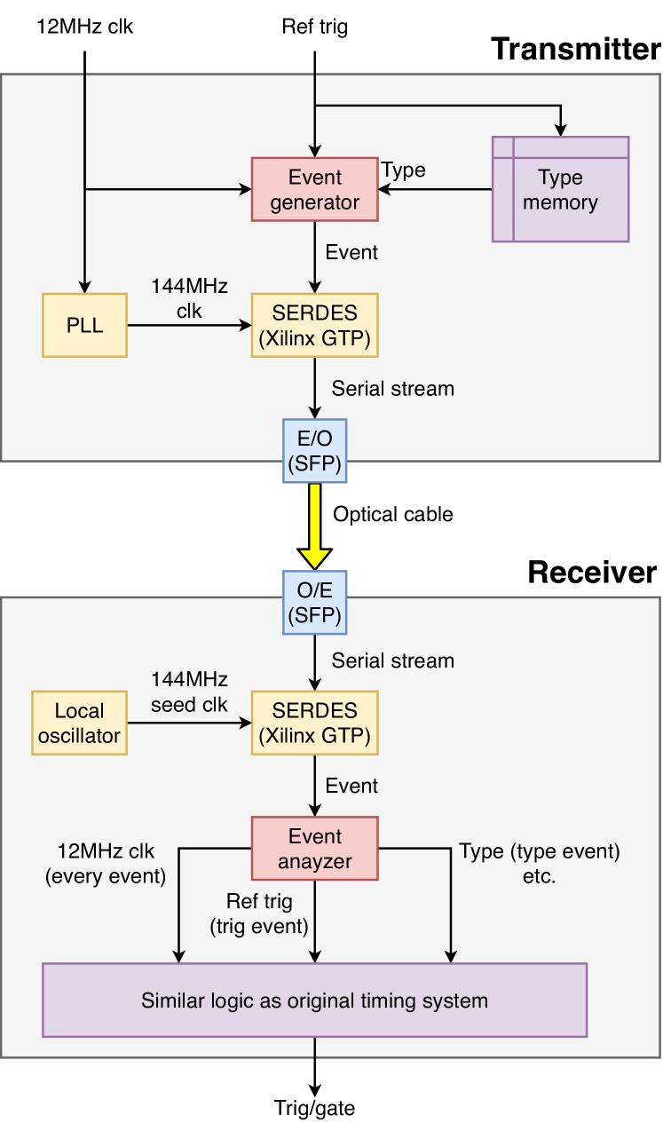
The new transmitter module generates an event, which is the payload of the high speed serial communication, every 12 MHz clock. Using the GTP [12], a high-speed communication transceiver in Xilinx FPGAs up to 3.2 Gbps, the generated events are serialized and sent via SERDES.
The new system is a kind of the event timing systems. The actual protocol of the serial communication to be sent is shown in Table I. In the 8B/10B conversion [13], there is the D-character, which is the actual 8-bit data, and the K-character with a special meaning. K28.5 is used in 8B/10B as a comma character to indicate the delimitation of a data sequence. An event is sent with a comma followed by data, E, that represents the meaning of the event, as shown in Table I LABEL:sub@tab:serial_format. The third through twelfth word can contain a total of 80 bits of data, if necessary. An event is a sequence of 12 consecutive 8 bits, which is converted to 8B/10B and transmitted at a transmission rate of 1.44 Gpbs.
When idle, the null event is constantly being sent. When the reference trigger is input to the new transmitter module, the trigger event is sent. In the type event, the third through sixth in the sequence contain type 1 through type 4 corresponding to mode 1 through mode 4, where the mode 2, mode 3, and mode 4 are for the linac, RCS, and MR, respectively. The type 1 for the mode 4 is reserved. In addition, S and S count values and the trigger count values that are transmitted by the original timing system are defined and transmitted as events, where S indicates the beginning of the MR cycle and the trigger count is the number of the reference 25 Hz triggers sent. Since the events can be defined in 256 ways, additional event types can be added and information can be sent as needed in the future.
The serialized data is converted to the optical signal by the SFP module, and delivered to the receiver module via the optical fanout and the optical cables.
The 144 MHz clock is decoded and the data is extracted using clock data recovery (CDR) by the GTP on the new receiver module. The decoded 144 MHz clock is perfectly synchronized to the clock used in the transmitter module. The received data is input to the event analyzer, The event is sent at 12 MHz repetition and the event analyzer generate 12 MHz clock using the events. The reference trigger is decoded in the trigger event, and the type code is decoded in the type event and supplied to the logic at the latter stage. The other events are also decoded. The logic of the latter stage is basically the same as that of the original receiver module and performs the same operation.
Thus, high speed serial communication makes it possible to transmit three types of signals over a single optical cable. It is important to note here that the GTP transceiver has slightly different delays at each power up. The delay change is one period of the clock input to the SERDES and is approximately 7 ns for the 144 MHz clock. This is not an acceptable change for the scheduled timing system. The recovered clock is generated by dividing the high speed serial clock, therefore several different phases are generated at each power up. To realize a fixed latency, a circuit configuration similar to that in Ref. [14] is required.
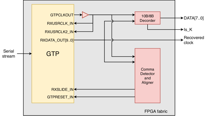
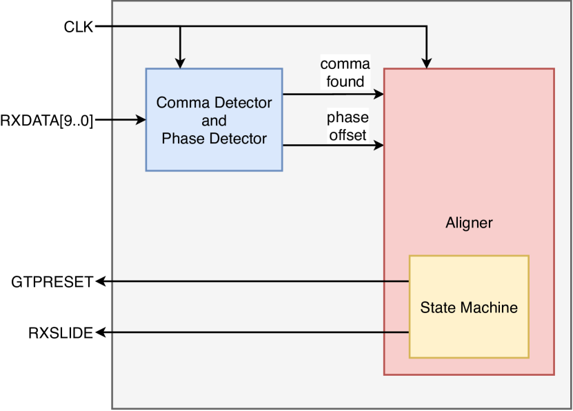
According to the reference, the comma detector and aligner (CDA) and the 10B/8B decoder for the receiver are implemented in the FPGA fabric, as shown in Fig. 7. The most important part of the implementation is the CDA functionality. The simplified block diagram of the CDA is shown in Fig. 8 The comma detector and phase detector block detects the phase misalignment by using the 10 bit RXDATA and the recovered clock. When the K28.5 comma is found, the comma found signal is asserted and the 4-bit phase offset information is sent to the aligner block. In the aligner, a state machine is running the following manner. If the phase offset in an even number of the unit intervals (UIs), the RXSLIDE signal, which generates the 2 UI phase shift of the recovered clock, is asserted for the necessary times. If it is an odd number, it is impossible to adjust the phase by the RXSLIDE. In this case the GTPRESET is asserted and the startup process of the GTP runs again. The reset is repeated until the misalignment becomes an even number. With the implementation, the delay is fixed at all power ups.
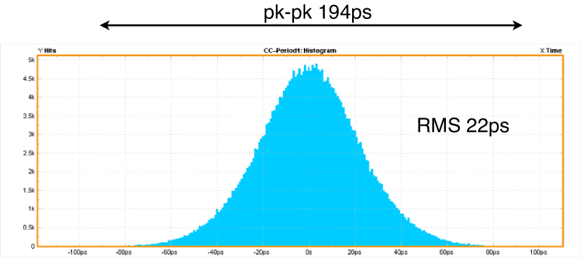
The jitter of the 12 MHz clock decoded by the new receiver module is important, because the 12 MHz clock is used not only as the reference for the 96 MHz delay counter clock but also for generating the system clock for the LLRF control system of the synchrotron. It has been examined the DPOJET of a Tektronics oscilloscope. The measurement result is shown in Fig. 9. The jitter is 22 ps for RMS and just under 200 ps for pk-pk, and sufficiently low to meet the requirements. The jitter of the trigger output is similar.
Since the next-generation system utilizes the high speed serial communication, the additional delay in the order of 250 ns compared to the original system is introduced. The additional delay is fixed value, therefore it is not problematic.
III-C New features of the transmitter module
As described in the previous subsection, the behavior of the new receiver module is basically the same as the original receiver module, while new features are implemented in the new transmitter module.
The length of the type memory in the original and new transmitter module is 512. the length corresponds to 20.48 s at the 25 Hz operation of the linac and 10.48 s at the 50 Hz operation, which is required for the future extension with the transmutation experimental facility (TEF)[15]. In both cases, the lengths can cover the MR cycle, up to 5.2 s. The number of the banks of the type memory is increased from 64 in the original module to 1024 in the new module. The linac will be operated at 50 Hz to inject the beams to the TEF and RCS alternatively. The extension of the memory bank is necessary to manage the increase of the combination of the operating patterns with the TEF.
For high intensity accelerators such as the J-PARC, a machine protection system [16] (MPS), which quickly stops the beam at machine failures, is indispensable to avoid damages of accelerator components due to the beam. A fast MPS was developed for the J-PARC [17, 18]. The J-PARC MPS can block the linac beam as quick as a few tens of s, by stopping the rf power to the RFQ (radio frequency quadrupole) at the beginning of the linac. The interlock signals are sent to the MPS main unit in the CCB, and the beam stop signal is generated and sent to the front-end of the linac. The failures that trigger the MPS are classified into three types, All-stop, MLF-inhibit [19], and MR-inhibit. The All-stop interlock, which stops the beams for both of the MLF and MR, is asserted with the failures at the linac and RCS, for example, the high level beam losses and the power supply failures. If a failure happens in the MLF, the MLF-inhibit interlock is raised, where the linac beams for the MLF are blocked and the beams for the MR are delivered to the RCS and MR. The process is similar to the MR-inhibit interlock.
The beam triggers for the beam instrumentation devices such as the beam position monitors and the current monitors should be stopped during the interlock, to avoid the loss of the measured beam signals, which can be used for the postmortem analysis of the beam or for the investigation of the machine failures. The beam triggers for the MR are suppressed by switching of the type sequence by software and that for the linac and RCS are stopped by modifying the LUT of the receiver modules via the RM networks. A new function, called the shift-jump function, is implemented in the new transmitter module, so that the suppression of the beam trigger is realized without the RM network.
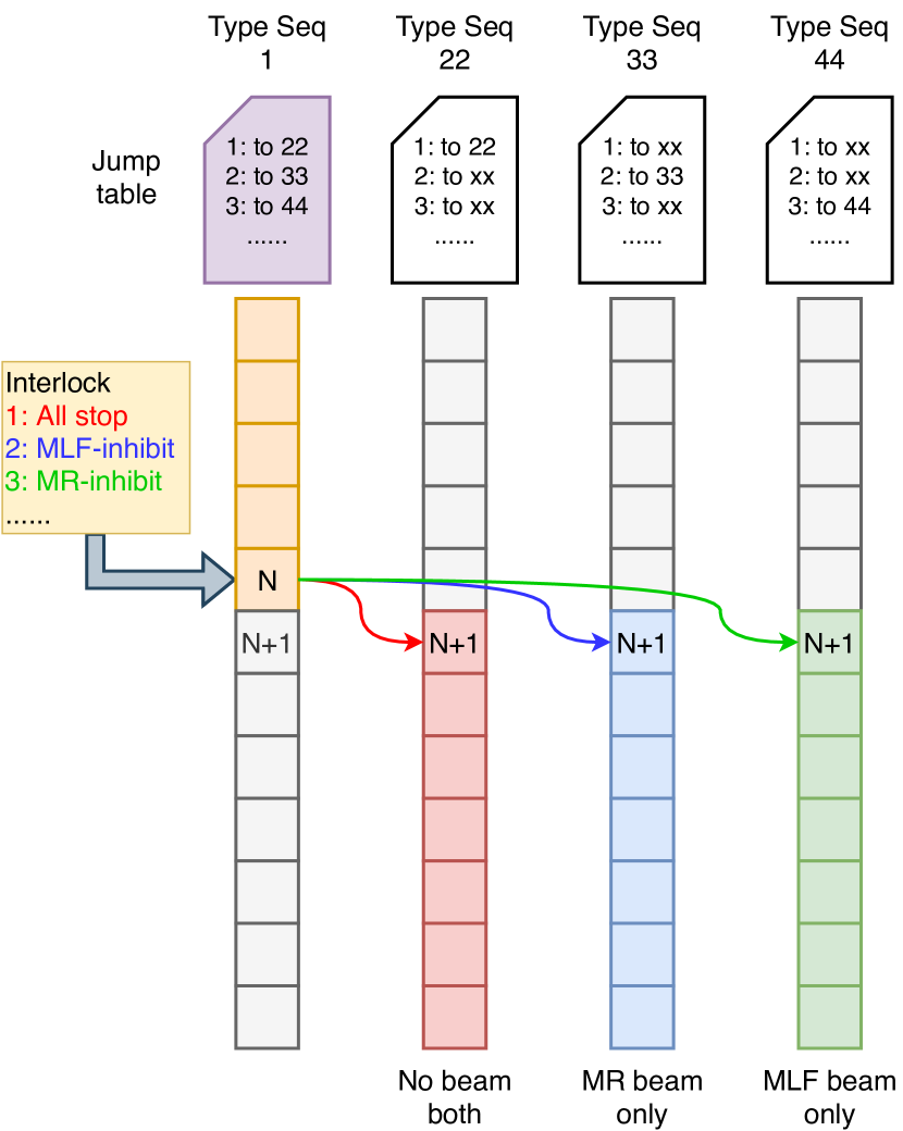
The operating principle of the shift-jump function is shown in Fig. 10. In the original transmitter module, the switching of the type sequence is allowed only when a single sequence is finished reaching the end code or the jump code to avoid corruption of the behavior. In the new module, the switching in the type sequence triggered by the interlock signals is newly defined. Each type sequence has a jump table, which defines the destinations related to the type of the interlocks. In the figure, we assume that Type sequence 1 is the sequence for the normal operation, where both of the MLF and the experiment of the MR are running. The interlock numbers of 1, 2, 3 correspond to the All-stop, MLF-inhibit, and MR-inhibit interlocks, and the destinations of the interlock numbers in the jump table of Type sequence 1 are defined as to 22, 33, and 44 respectively.
If an interlock is asserted at -th period, the type sequence is switched at -th period to the destination, according to the jump table. Type sequence 22 is composed by the type codes without the beams. Type sequence 33, which correspond to MLF-inhibit, consists of the type codes without the MLF beams. The case is similar for the case of Type sequence 44.
Thus, the suppression of the beam trigger is realized by the new shift-jump function without the RM network. The jump table must be carefully defined. The required number of type memory banks is also increased. This is another reason why the extension of the memory bank to 1024 is implemented.
Eight interlock inputs are prepared in the new transmitter module. Three interlocks are already defined as described above. Other five inputs are reserved.
III-D History and outlook
The development of the next-generation timing system was started in Japanese fiscal year (JFY) 2016, with prototyping on the Xlinx Spartan-6 evaluation kits, SP605. The new transmitter and receiver modules and the optical fanout were built based on insights gained from prototyping in JFY 2017–2018.
After extensive tests, the original transmitter module was replaced with new module in January 2020. Also, a few replacements of the receiver stations in the linac were made, where the noise environment is relatively severe and stabilization of the timing system is desired. The replacements were successful. The original receiver modules in the facilities that receive the signal from the new transmitter are running without issues as before and the new receiver modules are generating the triggers as expected.
As of September 2020, the replacements of 12 receiver stations with 28 new receiver modules in the linac and a reveiver station with 8 modules have been done. Additional 13 stations are to be replaced in JFY 2020. Three new power supply buildings in the MR have been constructed for the upgrades of the magnet power supplies toward the shorter repetition period [20]. The new PLC receiver modules are to be fully utilized in the new power supply buildings. The original VME receiver modules in the MR buildings will be updated with the PLC modules depending on the budget.
The shift-jump function of the new transmitter module is under testing. The function will be enabled for the normal user operation from this November.
IV Conclusion
The J-PARC timing system is designed to fit the operation of the accelerator complex, which has multiple beam destinations. The original scheduled timing system has been working without major problems, while the original system cannot be maintained for long term, due to the discontinued optical component. The next-generation timing system has been therefore developed.
The new system is developed with an emphasis on compatibility with the original system in terms of the operating principle. The signal transfer of the system is based on the high speed serial communication. Thanks to the CDR technology, three timing signals, the reference trigger, clock, and type code, are sent via a single optical cable. Particular consideration is given to realization of the fixed latency and the CDA and 10B/8B decoder are implemented in the FPGA fabric according to the reference [14]. Sufficiently low jitters of the clock and trigger are achieved.
New features are implemented in the new transmitter module. The shift-jump function is implemented so that the beam trigger can be stopped without the RM network when the interlock is asserted.
As designed to be compatible with the original system, the installation of the new receiver modules is progressing smoothly. The PLC receiver modules are to be installed in the new power supply buildings of the MR. The original VME receiver modules in the MR buildings will be replaced with the PLC modules depending on the budget.
The next-generation system is based on common serial communication technologies. The serial communication framework can still be implemented with the newer FPGAs, even if the current FPGA of the system is discontinued. Therefore, the system is expected to be sustainable.
Acknowledgments
We would like to thank the staffs of Hitachi Zosen Corporation, who implemented the timing modules. We are grateful to the J-PARC writing support group, which continuously encouraged us to write up this article. Also, we would like to thank all the members of the J-PARC. We acknowledge the late Prof. Junsei Chiba for his contribution to the design of the original J-PARC timing system.
References
- [1] “Accelerator technical design report for J-PARC,” JAERI-TECH 2003-044, 2003.
- [2] F. Tamura, H. Yoshikawa, J. Chiba, M. Yoshii, M. Tanaka, and S. Shimazaki, “J-PARC timing system,” in Proc. 9th Int. Conf. on Accelerator and Large Experimental Physics Control Systems (ICALEPCS’03),Gyeongju, Korea, 2003, pp. 247–249.
- [3] F. Tamura et al., “Timing system for J-PARC,” in Proceedings of the Particle Accelerator Conference (PAC 2005), 2005, pp. 3853–3855.
- [4] “MRF timing system,” http://www.mrf.fi/index.php/timing-system.
- [5] H. Takahashi, N. Hayashi, and M. Sugimoto, “Synchronized data distribution and acquisition system using reflective memory for J-PARC 3GeV RCS,” in Proceedings of 11th European Particle Accelerator Conference (EPAC 2008), Genoa, Italy, 2008, pp. 1553–1555.
- [6] H. Takahashi, M. Kawase, and N. Ouchi, “Application of trigger counter board for synchronized data,” in Proceedings of the 2nd International Symposium on Science at J-PARC (J-PARC 2014), 2015, p. 012020.
- [7] S. Itoh, K. Ueno, and T. Yokoo, “Fermi chopper developed at KEK,” Nuclear Instruments and Methods in Physics Research Section A, vol. 661, no. 1, pp. 58 – 63, 2012.
- [8] F. Tamura and M. Yoshii, “Stabilization of beam extraction timing in J-PARC RCS,” in Proceedings of 12th International Conference on Accelerator and Large Experimenal Physics Control Systems (ICALEPCS 2009), Kobe, Japan, 2009, pp. 647–649.
- [9] F. Tamura, M. Yoshii, A. Schnase, C. Ohmori, M. Yamamoto, M. Nomura, M. Toda, T. Shimada, K. Hara, and K. Hasegawa, “Achievement of very low jitter extraction of high power proton beams in the J-PARC RCS,” Nuclear Instruments and Methods in Physics Research Section A, vol. 647, no. 1, pp. 25 – 30, 2011. [Online]. Available: http://www.sciencedirect.com/science/article/pii/S016890021100951X
- [10] N. Kamikubota, N. Kikuzawa, F. Tamura, and N. Yamamoto, “Operation status of J-PARC timing system and future plan,” in Proc. 15th Int. Conf. on Accelerator and Large Experimental Physics Control Systems (ICALEPCS’15), Melbourne, Australia, 2015, pp. 988–991.
- [11] M. Lipiński, T. Włostowski, J. Serrano, and P. Alvarez, “White rabbit: a PTP application for robust sub-nanosecond synchronization,” in 2011 IEEE International Symposium on Precision Clock Synchronization for Measurement, Control and Communication, 2011, pp. 25–30.
- [12] Xilinx, “Spartan-6 FPGA GTP transceivers user guide,” https://www.xilinx.com/support/documentation/user_guides/ug386.pdf.
- [13] “Method and apparatus for encoding binary data,” U.S. Patent 4,456,905, 1984.
- [14] R. Giordano and A. Aloisio, “Fixed-latency, multi-gigabit serial links with Xilinx FPGAs,” IEEE Transactions on Nuclear Science, vol. 58, no. 1, pp. 194–201, Feb 2011.
- [15] T. Sasa, “Design of J-PARC transmutation experimental facility,” in Nuclear Back-end and Transmutation Technology for Waste Disposal. Springer, Tokyo, 2015, pp. 73–79.
- [16] R. Schmidt, “Introduction to Machine Protection,” in 2014 Joint International Accelerator School: Beam Loss and Accelerator Protection, Newport Beach, CA, USA, pp. 1–20.
- [17] J. Chiba, K. Furukawa, N. Kamikubota, T. Katoh, H. Nakagawa, K. Niki, J. Odagiri, Y. Takeuchi, N. Y. K. M. Furuse, Y. Kato et al., “Present status of the j-parc control system,” in Proc. 9th Int. Conf. on Accelerator and Large Experimental Physics Control Systems (ICALEPCS’03),Gyeongju, Korea, 2003, pp. 1–5.
- [18] H. Sakaki, N. Nakamura, H. Takahashi, and H. Yoshikawa, “Design of the prototype-unit for j-parc machine protection system (in Japanese),” JAERI-TECH 2004-022.
- [19] K. Sakai, T. Kai, M. Ooi, A. Watanabe, T. Nakatani, W. Higemoto, S.-i. Meigo, S. Sakamoto, H. Takada, and M. Futakawa, “Operation status of interlock system of Materials and Life Science Experimental Facility (MLF) in J-PARC,” Progress in Nuclear Science and Technology, vol. 4, pp. 264–267, 2014.
- [20] T. Koseki, “Upgrade Plan of J-PARC MR - Toward 1.3 MW Beam Power,” in Proc. 9th International Particle Accelerator Conference (IPAC’18), Vancouver, BC, Canada, April 29-May 4, 2018, ser. International Particle Accelerator Conference, no. 9. Geneva, Switzerland: JACoW Publishing, June 2018, paper TUPAK005, pp. 966–969, https://doi.org/10.18429/JACoW-IPAC2018-TUPAK005. [Online]. Available: http://jacow.org/ipac2018/papers/tupak005.pdf