Misfit layer compounds: a platform for heavily-doped two-dimensional transition metal dichalcogenides.
Transition metal dichalcogenides (TMDs) display a rich variety of instabilities such as spin and charge ordersMonceau (2012); Wilson et al. (1975), Ising superconductivity Yuan et al. (2014); Lu et al. (2015); Xi et al. (2016a); Zhou et al. (2016); Hsu et al. (2017) and topological properties Qian et al. (2014a); Fei et al. (2017). Their physical properties can be controlled by doping in electric double-layer field-effect transistors (FET). However, for the case of single layer NbSe2, FET doping is limited to cm-2 Xi et al. (2016b), while a somewhat larger charge injection can be obtained via deposition of K atoms. Here, by performing ARPES, STM, quasiparticle interference measurements, and first principles calculations we show that a misfit compound formed by sandwiching NbSe2 and LaSe layers behaves as a NbSe2 single layer with a rigid doping of electrons per Nb atom or cm-2. Due to this huge doping, the charge density wave is replaced by a order with very short coherence length. As a tremendous number of different misfit compounds can be obtained by sandwiching TMDs layers with rock salt or other layers Wiegers and Meerschaut (1992); Wiegers (1996), our work paves the way to the exploration of heavily doped 2D TMDs over an unprecedented wide range of doping.
I Introduction
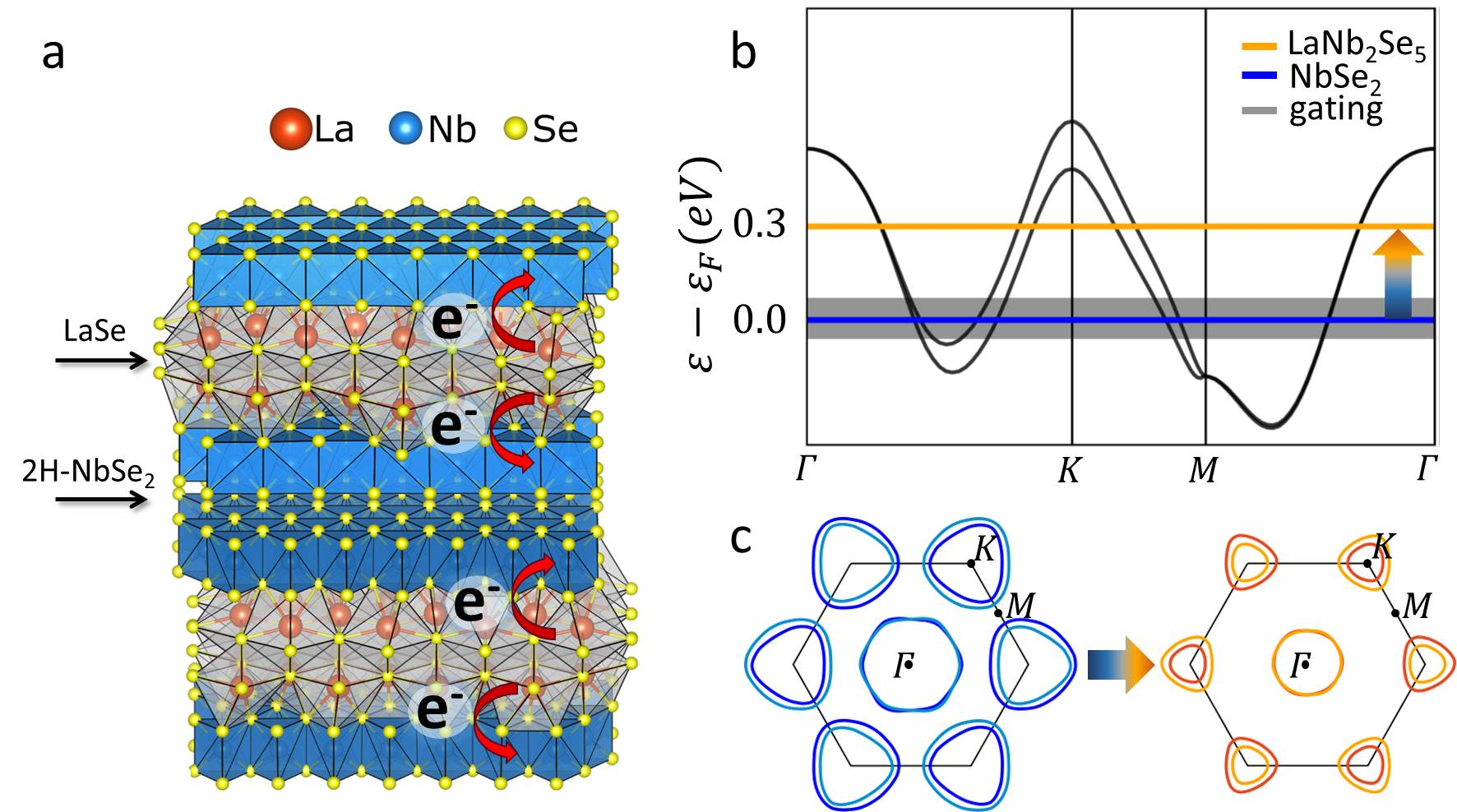
TMDs are layered materials with strong in-plane bonding and weak, van der Waals-like, coupling between the layers Wilson et al. (1975). They exhibit a rich physics with many kinds of electronic orders such as charge density wave or superconductivity Monceau (2012); Klemm (2011). In this family, single layer NbSe2 attracted a considerable interest as it presents a charge density wave instability with periodicity Xi et al. (2015); Ugeda et al. (2016) and a strong spin-orbit interaction leading to spin-momentum locking in the out of plane direction generating fully spin up and spin down polarized bands at K and K’ (see Fig. 1) Xiao et al. (2012); Kormányos et al. (2013); Bawden et al. (2016). This peculiar spin-orbit interaction has led to new developments in the field of non-conventional superconductivity, as recent measurements on monolayer and few layers NbSe2 samples showed that the in plane critical magnetic field is much larger than the paramagnetic limitKhestanova et al. (2018); Xi et al. (2016a). It has been shown that both phase transitions can be partially tuned by applying a gate voltage Xi et al. (2016b); Lu et al. (2015). It is thus crucial to study the evolution of charge ordering and superconductivity in 2D metallic dichalcogenides in the limit of heavy electron-doping, going way beyond what can be achieved by FET doping techniques (see Fig. 1).
Most of the studies on few layers NbSe2 were done using mechanicalNovoselov et al. (2005) or liquid exfoliation Coleman et al. (2011) which implies finding a flake of sample of the appropriate thickness among the many pieces dispersed on a substrate. Doping is then achieved via FET or adatom deposition. Here, we propose an alternative technique that allowed us to investigate the extreme high-doping limit of a NbSe2 single layer. We propose to use a compound belonging to the misfit TMDs. These misfits materials consist of transition metal dichalcogenides layers sandwiched with rock salt chalcogenides layers Rouxel et al. (1995), namely (RQ)1+x(TQ2)n (R=Pb, Bi or Rare-Earth, Q=Chalcogene, T=Transition metal and ) (see Figs. 1 and 2) which exhibit an intergrowth structure formed by the alternated stacking of RQ planes (having NaCl structure) with TMD layers (CdI2 or NbS2 structure). An electronic charge transfer occurs from the RQ to the TMD layers stabilising the structure. It was suggested that these compounds could be considered as intercalated compounds, however it is unclear if a rigid band model of doping could apply Cario et al. (1997, 1999). It is possible to obtain a large variety of multilayers of TMDs (1, 2 or 3 layers) separated by insulating RQ layers. For instance, the (LaSe)1.14(NbSe2)2 compound is composed by metallic 2H-NbSe2 bilayers separated by insulating LaSe bilayers (Figs.1 and 2). It is even possible to use multilayers of RQ in order to get quasi-2D non coupled NbSe2 multilayers, thus realizing nearly ideal embedded 2D systems with a well-defined multilayer structure.
Many misfits layered compounds were found to be superconducting, like (PbS)1.14NbS2 or (LaSe)1.14(NbSe2)2 Rouxel et al. (1995) with K and K respectively. (LaSe)1.14(NbSe2)2 displays an in-plane critical field around 30 T way beyond the 11.5 T paramagnetic limit required to break singlet Cooper pairs. A similar compound (LaSe)1.14(NbSe2), consisting of a stacking of 1H-NbSe2 and LaSe single layers, has a critical temperature of 1.2 K and a huge in-plane critical field of more than 16 T, which is well beyond the paramagnetic limit of 2.6 T Monceau et al. (1994); Kačmarčík et al. (2000, 2004); sofranko_periodic_2020. This enhanced critical field is similar to what was reported for few layers NbSe2 Xi et al. (2016a) and gated MoS2 Lu et al. (2015). These unusual superconducting properties indirectly suggest that the material behaves similarly to monolayer NbSe2 making it a bulk yet quasi-2D system. However, up to now there is no direct evidence of its bidimensionality and no measurement of the amount of doping in NbSe2 layers.
Here we show that (LaSe)1,14(NbSe2)2 hosts indeed a band structure that is intimately related to the one of a strongly and rigidly doped NbSe2 monolayer. We measured finely the Fermi surface using quasiparticles interferences (QPIs) spectroscopy and ARPES. Our measurements, supported by extensive first-principles DFT calculations, demonstrate that (LaSe)1,14(NbSe2)2 behaves as a heavily electron-doped monolayer NbSe2 with a Fermi level shifted of +0.3 eV, or equivalently electron per niobium atom.
The general idea of our work is summarized in Fig. 1 (b) where the band structure of 1H-NbSe2 monolayer is shown in black and the chemical potential of the undoped monolayer in blue. The gray ribbon labels the range of doping achievable with ionic liquid gatingXi et al. (2016c). It has to be compared with the level of doping achieved in the misfit compound via electronic charge transfer from the LaSe to the NbSe2 layers, shown in yellow. This tremendous doping is several times larger than what can be achieved by conventional ionic liquid doping in field effect transistor geometry. As a consequence, the shape of the Fermi surface is greatly modified and in particular the Fermi pockets at and K are strongly shrunk as our quasiparticle interferences and ARPES measurements reveal. The ability to induce a huge doping such as to change dramatically the shape of the Fermi surface is extremely promising for future work on electronic properties of misfit compounds.
II Structure
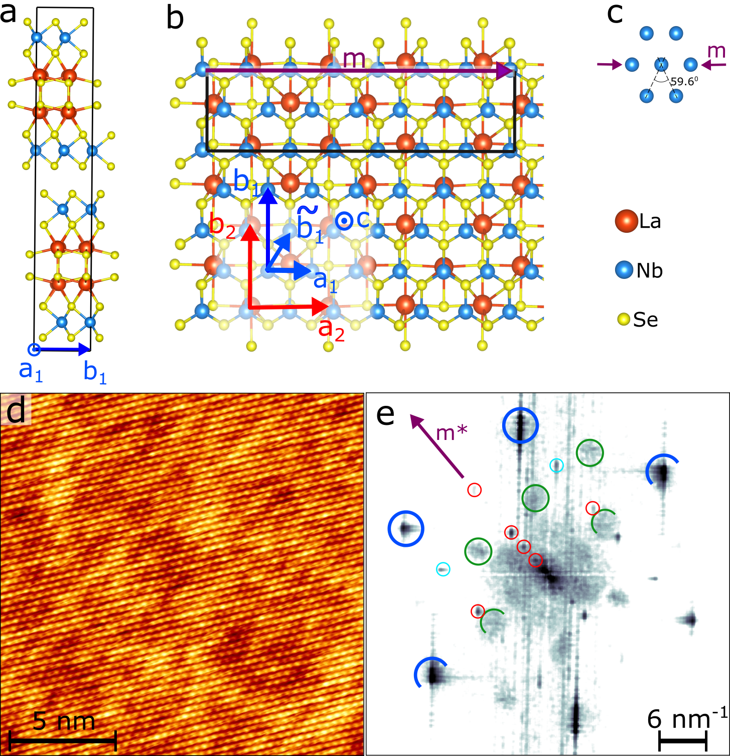
The misfit material (LaSe)1,14(NbSe2)2 is a layered compound consisting of a regular alternation of 2H-NbSe2 bilayers with trigonal prismatic structure and of rocksalt two atom thick LaSe layers (Figs. 1-2). Each NbSe2 and LaSe sublattice has its own set of cell parameters noted , and with =1 and 2, respectively. Compared to bulk 2H-NbSe2 the lattice of NbSe2 layers is not perfectly hexagonal and is slightly compressed along the direction (space group C2221, see Fig. 2(c)). As a consequence the NbSe2 sublattice is described by a centered orthorhombic cell with in plane lattice vectors Å and Å. The LaSe sublattice has also an orthorhombic symmetry but with similar in plane lattice parameters Å. Both NbSe2 and LaSe layers have the same lattice vector (=) and the material is commensurate in this direction. However, the ratio between the norms of the and vectors, sharing a common direction, is an irrational number (), making (LaSe)1,14(NbSe2)2 incommensurate in the direction. However, such that (LaSe)1,14(NbSe2)2 can be considered as almost periodic in the direction with an approximate commensurate lattice vector ().
A commensurate structure with was assumed in first principles electronic structure calculations (see the method section). We performed structural optimization for the full bulk structure (232 atoms per cell). We used different starting guesses obtained by superimposing in different ways LaSe and NbSe2 bilayers (see SI). Minimization of the total energy gives two inequivalent minima that however result in very similar structures with practically identical electronic structures. Very strong iono-covalent bonds form at the contact between NbSe2 and LaSe with a substantial deformation of the LaSe layer (see Fig. 2 and movie in SI) and a significant deviation from an ideal rock salt structure. This huge modification of the LaSe interface signals a large charge transfer between LaSe and NbSe2 bilayers. On the contrary the van der Waals interface between the two NbSe2 layers is weakly affected. This explains why the cleavage of the sample leads to a monolayer (ML) NbSe2 terminated surface (see Figs. 1-2) that we probed by STM and ARPES.
A typical STM topography map of (LaSe)1,14(NbSe2)2 surface of an in situ cleaved sample is represented in Fig. 2 (d). Since the surface layer is 1H-NbSe2 , the atomically resolved STM images show the Se atoms of NbSe2. The rectangular centered Se lattice appears almost hexagonal and for simplicity, in the following, the NbSe2 layers will be referred as hexagonal. In addition to the Se atomic lattice, one observes multiple additional spatial modulations which are due to the incommensurability with the underlying LaSe layer. In order to properly characterize the origin of these modulations, the modulus of the Fourier transform of a similar but larger scale topographic image taken on the same area with same scanning angle is represented in Fig. 2 (e). The Bragg peaks of the reciprocal lattice of NbSe2 are highlighted by blue circles. The sharp peaks circled in red are the first, second, third and sixth harmonics of the approximate periodic misfit potential. Additional peaks attributed to the LaSe lattice are also observed and accented by light blue circles. The signals presented so far can directly be deduced from the theoretical crystalline structure. In addition to those, one can also observe other contributions. First, diffuse peaks (highlighted by green circles) lie at half the Bragg peaks of the NbSe2 hexagonal lattice. They express the presence a charge modulation in the system. This charge order will be fully discussed later in this paper. In addition, a halo surrounding quasi-reaching half the Bragg peaks can be seen. It is attributed to integrated quasiparticle interference spectroscopic signal as we discuss below.
III Electronic band structure
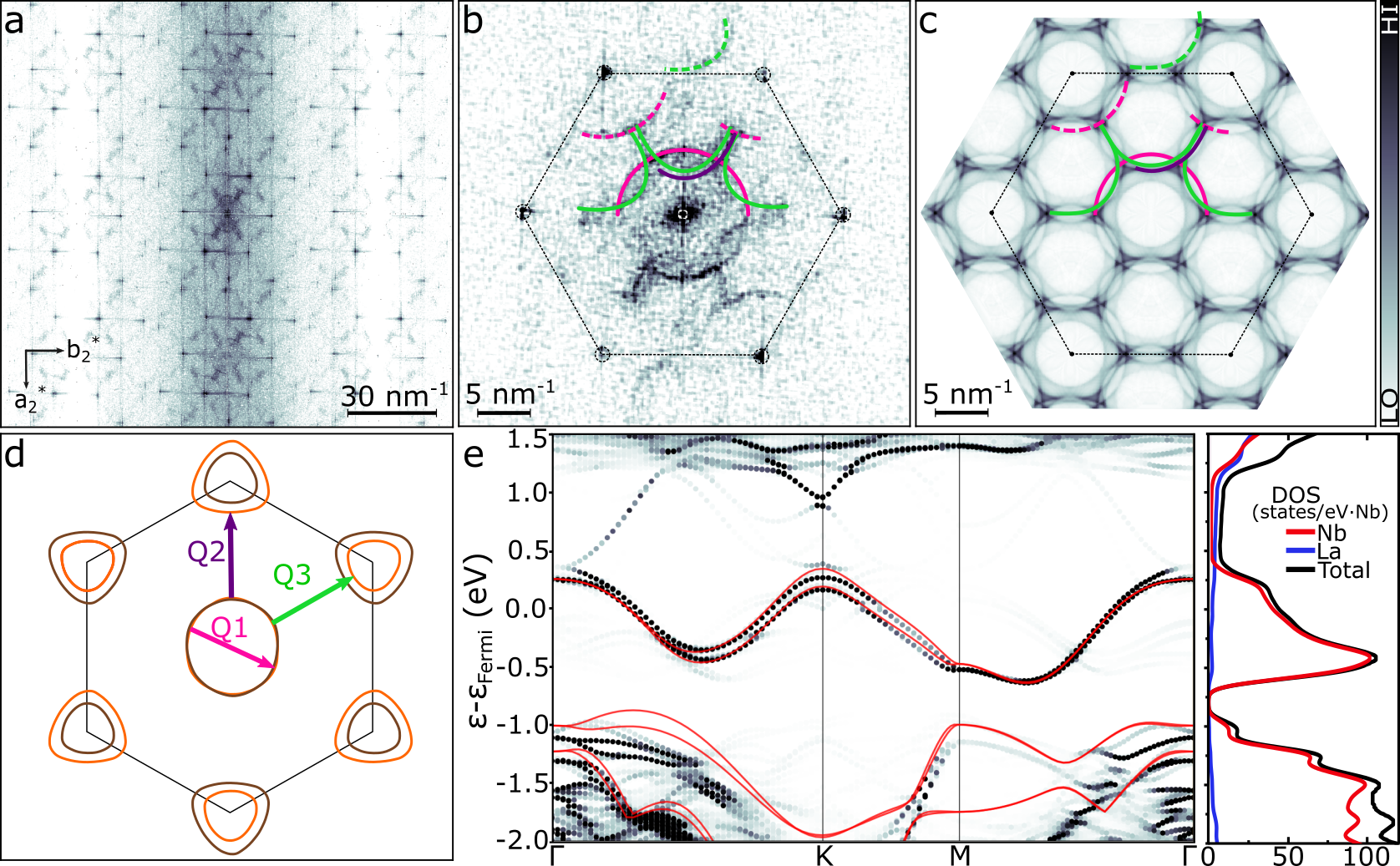
We then study the electronic structure of the surface of NbSe2 terminated (LaSe)1,14(NbSe2)2 by using DFT calculations. The results are presented in Fig. 3 (e) after band unfoldingMedeiros et al. (2014, 2015) onto the NbSe2 three-atom C2221 pseudo-hexagonal unit-cell having Å and Å(, see Fig.2 (b)). As a reference, we also plot in red the electronic structure of an isolated 1H-NbSe2 layer with the same and but doped by electrons per Nb atom (we use a compensating positive background to ensure charge neutrality). As it can be seen, the electronic structure of (LaSe)1,14(NbSe2)2 in a eV range from the Fermi level is almost indistinguishable from that of a rigidly doped NbSe2 monolayer. This is further confirmed by the detailed comparison of the electronic structure of the (LaSe)1,14(NbSe2)2 surface with that of a rigidly-doped single layer NbSe2 with C2221 unit cell (see Figs. S1 and S2 in SI). The only differences occur at zone center where a lanthanum band hybridizes with the single layer NbSe2 band. The resulting band deformation leads to a small La component at the Fermi level () close to zone center. The amount of La electrons at remains, however, negligible, as demonstrated by the density of states projected over La and Nb atomic states in the rightmost panel of Fig. 3 (e). Finally, we underline that, even if we keep in all simulations the non-perfect hexagonal symmetry due to the anisotropy in and , this effect is completely irrelevant and does not lead to any sizeable effect in the electronic structure and Fermi surface. The calculated Fermi surface of the isolated layer is plotted in Fig. 3 (d) with the degree of spin up and down polarization illustrated in different colors.
We probed the band structure at Fermi energy by quasiparticle interference spectroscopy measurements on NbSe2 terminated (LaSe)1,14(NbSe2)2 . This technique relies on the scattering of the electron Bloch functions by defects. The incoming and scattered electrons may give rise to some interference pattern that can be measured by scanning tunneling spectroscopy. In Fig. 2(e) some QPIs are already appearing, but they are not well resolved. This is due to the fact that the topography was recorded with a bias of 200 mV and, as such, it is sensitive to the integral of the local density of states in an energy window of 200 meV. Thus the spectroscopic halo around in Fig. 2(e) is actually a mix between the QPIs patterns at all energies ranging from 0 meV to -200 meV. In order to get a highly resolved QPIs measurement of the band structure at the Fermi energy we performed topography measurements with a low voltage of 20 mV so that only electrons in a 20 meV window close to contributed (Fig. 3 (a)). As the band dispersion over a 20 meV range is negligible (see Fig. 3 (e)), these measurements should reflect the joined density of states at the Fermi level (see method section). The Fig. 3 (a) shows a Fourier transform of the topography which spans many Brillouin zones. One can observe a dark vertical band which indicates that a stronger QPI signal is generated in the direction of the incommensurability. This suggests that the incommensurability plays the role of electron scattering potential. Moreover, as atomically resolved images in Fig. 2 do not present any visible defects such as vacancies, steps or dislocations (i.e. the samples are very clean), the only scattering mechanism susceptible to generate QPIs is provided by the incommensurability.
In order to get more insight on the band structure we performed QPIs measurements by taking the squared modulus of Fourier transform of conductance maps measured at the Fermi energy. Such a QPIs measurement is shown in Fig. 3 (b), where one can see a complex structure with some almost circular patterns. The different circular patterns are associated to different scattering mechanisms shown in Fig. 3 (d). For instance the vector depicts scattering events from the pocket to itself, while depicts scattering between the pocket and the outer K or K′ pockets. Finally, the vector schematizes scattering in between and the internal K and K’ pockets. These different scattering channels lead to the nearly circular patterns depicted in color on Fig. 3 (b). We calculated the QPI patterns (see methods and SI) by using DFT for a three atoms NbSe2 unit cell for an unsupported monolayer with a doping of electrons per Nb atom. The simulated QPI, shown in Fig. 3 (c) exhibits the same circular patterns as the experiment. In order to compare quantitatively the experimental and theoretical QPIs we plotted an identical set of circles on both Figs. 3 (b) and (c), where the color corresponds to different scattering channels as explained above. The agreement is very good; all the patterns observed experimentally are accurately reproduced by the rigid band approximation of 1H-NbSe2 monolayer doped by electrons per Nb, except some spectral weight at the Bragg peaks. This latter electron doping agrees well with the chemical estimate that, in (LaSe)1,14(NbSe2)2, the (LaSe)1,14 should provide 1.14 electrons to (NbSe2)2. This simple chemical intuition leads to 0.57 electron doping which is in very good agreement with DFT and experiments.
One of the major interests of single layers 1H TMDs is their Ising spin orbit splitting. This spin orbit splitting should manifest with two scattering channels corresponding to the scattering from to the outer K pocket and from to the inner K pocket, represented schematically by and , respectively in Fig. 3 (d). This should lead to two concentric circles schematized by the purple and green arcs in Figs.3 (b) and (c). This splitting is indeed observed even though the signal to noise ratio is pretty weak.
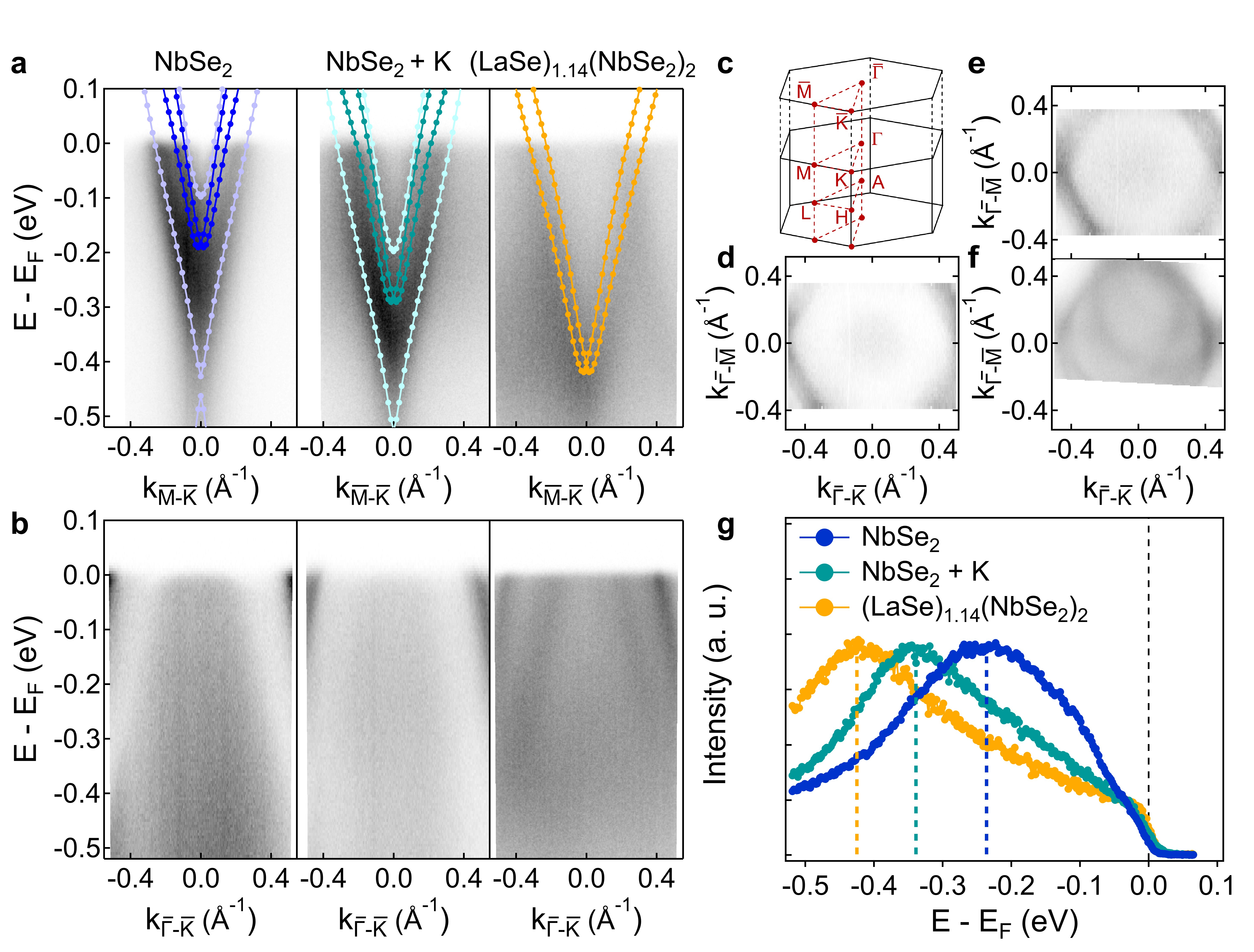
According to our QPIs measurements and DFT calculations we found that the band structure of the NbSe2 terminated surface of (LaSe)1,14(NbSe2)2 is well accounted for by a rigid band approximation with a huge Fermi level shift. In order to ascertain this finding, we carried out some comparative ARPES measurements of the low-energy electronic states of bulk 2H-NbSe2, K-doped 2H-NbSe2 (see Methods) and (LaSe)1.14(NbSe2)2 at T=50 K and using He-I radiation (= eV). Figures 4 (a) and (b) show the corresponding ARPES intensity maps along the -- and -- high-symmetry lines of the hexagonal surface Brillouin zone of 2H-NbSe2 (Fig. 4 (c)), respectively. Around , for pristine 2H-NbSe2 (Fig. 4, left panel), we can easily recognize the spin-polarized Nb 4-derived states coming from the cut of the two strongly trigonally-warped barrels of the Fermi surface centred around each zone-corner () point (also see the calculated Fermi surfaces in Fig. 3) Bawden et al. (2016). At (Fig. 4 (b), left panel), whereas the Nb-dominated states yield strong spectral weight close to the Fermi level crossings away from normal emission, additional diffuse spectral weight coming from a highly three-dimensional Fermi surface sheet of predominantly Se orbital character is visible at the zone centre due to the finite out-of-plane momentum resolution of ARPES (also see the measured Fermi surface Fig. 4 (d)) Bawden et al. (2016).
The same spectral features are also seen for the K-saturated surface of NbSe2 with a yet higher diffuse background (coming from the randomly adsorbed alkali atoms at the NbSe2 surface) and a different chemical potential as evidenced by the shift towards higher binding energies of both the electron pocket at and the hole pocket at (Fig. 4 (a) and (b), middle panels) and the reduced area of the -centred Fermi surface (Fig. 4 (e)). As at the photon energy used here, the inelastic mean free path of the photoelectrons is on the order of the interlayer distances, we are predominantly sensitive to the doping of the topmost layer of the unit cell. From our ARPES measurements, we can thus conclude that the K-saturated NbSe2 surface has been electron-doped within a rigid-band picture corresponding to a chemical potential shift of 100 meV.
Focusing now on (LaSe)1.14(NbSe2)2, we observe further energy shifts towards higher binding energy of both the electron and hole Nb-derived pockets (Fig. 4 (a) and (b), right panels) as well as a still reduced Fermi surface area (Fig. 4 (f)). This indicates that the electron-doping of the NbSe2 layer at the interface with LaSe within the misfit compound is much higher than the one obtained by alkali gating. Energy distribution curves taken at the point for bulk NbSe2, K-doped NbSe2 and (LaSe)1.14(NbSe2)2 (Fig. 4 (g)) demonstrate that such a doping is almost twice the one reached in K-doped NbSe2 with a chemical potential shift of 190 meV (see the vertical dashed lines on Fig. 4 (g) showing the energy position of the bottom of the electron pockets at ) with respect to pristine NbSe2. Interestingly, we can also note the absence of spectral intensity coming from the Se orbital at the zone centre (Fig. 4 (b). right panel), indicating that the band structure of NbSe2 within the misfit compound is close to the one of a strongly electron-doped NbSe2 monolayer. Nevertheless, the electrons feel a rather strong competing potential coming from the intrinsic incommensurability of the heterostructure as evidenced by the clear presence of shadow bands not only in the ARPES intensity maps but also at the Fermi surface (Fig. 4 (f)).
IV emergence of charge ordering
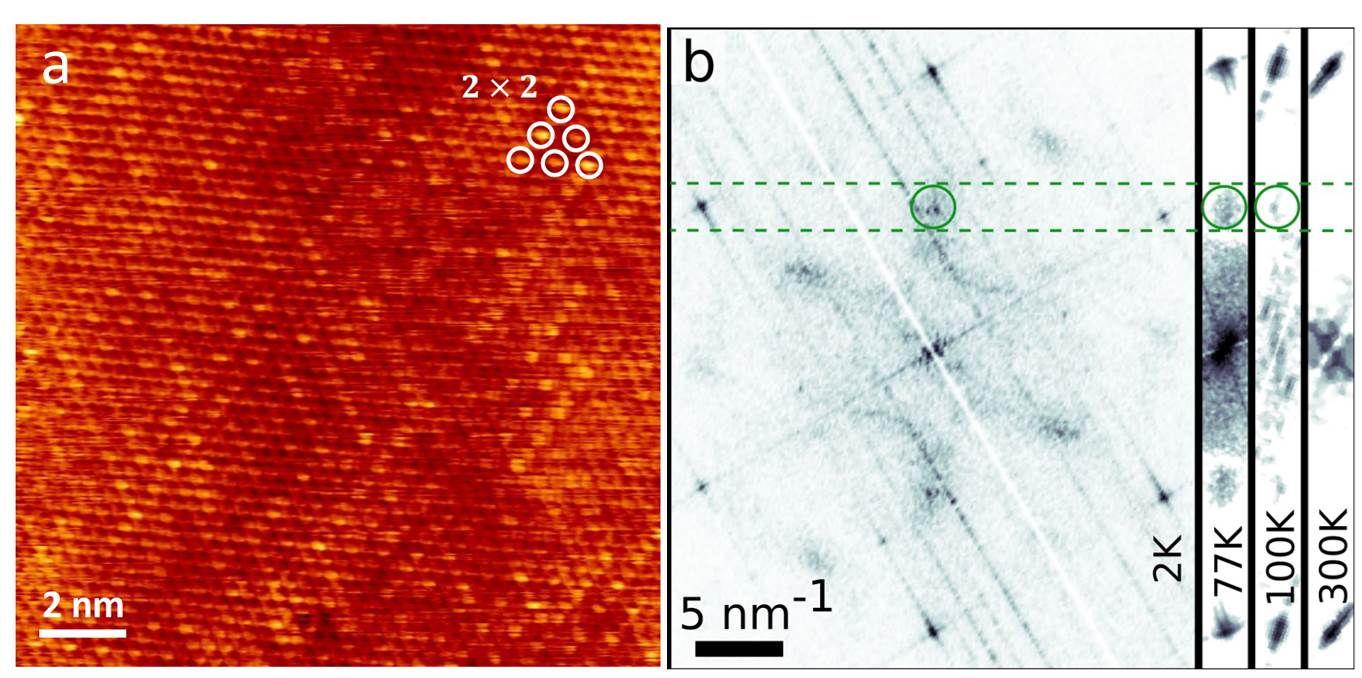
Bulk 2H-NbSe2 shows a charge density wave (CDW) transition at around 35 K with a nearly commensurate charge orderWilson et al. (1975). In single layer, contradictory results have been reported as ML NbSe2 on top of Graphene shows a strong increase of TCDW with respect to the bulkXi et al. (2015), while ML NbSe2 grown on top of SiO2 shows a CDW with a similar TCDW as in the bulk. Recent first principles calculationsBianco et al. (2020) confirm the second behaviour. It has been shown that electron doping by FET strengthen TCDW Xi et al. (2016b), it is however unclear if a change of ordering vector occurs. The continous TCDW curve versus FET doping in RefXi et al. (2016b) seems to suggest that it is not the case, however the range of considered doping is much lower.
Since (LaSe)1,14(NbSe2)2 shows an energy band structure analogous to 1H-NbSe2 monolayer one expects CDW to show up at low temperatures. It is well established that CDW are in general very sensitive to the shape of the Fermi surface. Thus, one expects that the strong doping of electrons/Nb could induced some change in the CDW periodicity. This is indeed the case as we found no experimental evidence of a charge ordering, but we find patches appearing below approximately 105 K in most parts of the sample. Our experimental observations are summarized on Fig. 5, where a topography with a charge order is shown in panel (a), while the Fourier transform modulus of the topographies measured at various temperature are shown in (b). The Fourier transform shows a six-fold peak structure at half-Bragg positions that corresponds to a charge modulation in real space. The signal is still present in Fourier map at 100 K and it disappears above 105 K see Fig. 5 (b). However, the reconstruction does not cover completely the sample in a uniform way, but is more clearly visible in some regions with respect to others. The corresponding CDW peak in Fig. 5 is also less sharp, probably meaning that regions of ordering coexist with patches with no CDW ordering.
In order to investigate the possible evolution of TCDW with doping, we performed harmonic phonon calculations using density functional perturbation theory Giannozzi et al. (2009, 2017) for a single layer NbSe2 as a function of electron doping. The system is kept neutral by using a positive jellium background. The hexagonal-compression of the lattice is included, so that there are two inequivalent points (labeled and ). The results are shown in SI, Fig. S3. At zero doping, we find a broad region of instability close to and , compatible with a CDW, signaled by the occurrence of an imaginary mode both along and . At a doping of electrons/Nb, the region of instability shifts at the and points, in qualitative agreement with experimental findings. It is known that Bianco et al. (2020) the CDW in NbSe2 arises from an interplay between Fermi surface effects and ionic fluctuations related to anharmonicity. Fermi surface effects determine the ordering vector, while the occurrence of the CDW is mostly related to phonon-phonon scattering. In our calculation we only include harmonic terms, thus we overestimate the tendency towards CDW. At a doping of electrons/Nb, the ordering vector changes essentially because the Fermi surface geometry is affected and a nesting compatible to reconstruction occurs. However, at the doping of electrons/Nb, that is the one estimated by comparing our electronic structure with QPI and ARPES, no instability is found, mainly because the vector does not connects efficiently portion of the Fermi surface. Anharmonicity would suppress even more the CDW instability. A possible way to reconcile theory and experiments, is to consider a non-uniform doping in the sample and the possible existence of patches with lower doping. These regions are not detected in ARPES and QPI that probe larger regions of the sample, however they can be detected by the ultrafine spatial sensitivity of STM.
V Conclusion
The success of two dimensional crystals in the fields of physics, nanotechnology, chemistry and material science is largely due to the much greater tunability of their properties with respect to their bulk counterparts. The three main parameters that can be varied are the sample thickness, the Moiré angle between the stacked layers and doping. However, while the first two parameters can be varied at will, for NbSe2 doping is limited to electrons cm-2Xi et al. (2016c), that is the maximum amount of carriers that can be introduced in an electrical double-layer field-effect transistor geometry. Somewhat larger doping can be achieved via deposition of Alkali atoms (such as potassium). However, in many cases, the deposition of alkali atoms on a 2D crystal is difficult to achieve as the coverage can be non-uniform or the wetting of the 2D crystal by the adatoms not even possible.
Here we propose to use rocksalt rare-earths chalcogenides sandwiched with transition metal dichalcogenides to build a misfit compound. Both the thickness of the transition metal dichalcogenide and of the rocksalt rare-earth chalcogenide can be tuned at will Wiegers and Meerschaut (1992); Wiegers (1996), exactly as in a 2D crystal. The large electron charge transfer from the rare-earth chalcogenide to the TMD allows to obtain doping fractions that largely encompass both those obtained in the case of ionic-liquid-based field-effect transistors and K adatom deposition. We have shown that this is indeed the case for NbSe2 bilayers sandwiched in rocksalt LaSe for which we achieve a doping of electrons per Nb, corresponding to a eV shift of the Fermi level. This large electron transfer from LaSe to the TMD is due to the chemical properties of the highest occupied states of bulk LaSe that are formed only by atomic La statesPersson (2014). As a consequence LaSe essentially behaves as a donor, an effect that we expect not to depend on the kind of TMD used to build the misfit structure. This suggests that similarly large doping can be achieved by sandwiching LaSe with other metallic TMDs.
Finally, we remark that it is also possible to vary the rocksalt layer, opening a tremendous space of possibilities and a fertile ground for the discovery of highly innovative materials. For instance, assuming La3+, Pb2+ and Se2- in the hypothetical series of compounds (La1-yPbySe)1+x(NbSe2)2 a simple charge balance calculation shows that the charge transfer from the rock salt layer (La1-yPbySe) to the (NbSe2)2 double layer could vary continuously from to by reducing the lead content. While the (La1-yPbySe)1+x(NbSe2)2 series was never reported so far, similar substitutions of La3+ per Sr2+ substitution were already demonstrated in the (LaS)1+xVS2 Nishikawa et al. and (LaS)1+xCrS2 Cario et al. (1997). Therefore, the charge transfer could be tuned by appropriate substitution in misfit layer compounds, pretty much in the same way as doping can be varied in field-effect transistor, but in a much broader range.
We have shown that the effect of a large electron doping in single layer NbSe2 results in the change of the ordering vector of the charge density wave. However, other properties can also be explored in misfit compounds, such as topological and Ising superconductivities in NbSe2 and MoS2, Mottronics with misfit compounds involving 1T-TaSe2 or 1T-NbSe2 layers Janod et al. (2015); Nakata et al. (2016); Colonna et al. (2005) or thermoelectric applications Xu et al. (2014); Rameshti and Asgari (2016); Qian et al. (2014b) where the ability to fine tune the chemical potential in stacks of 2D topological insulators such as 1T′-WSe2 would be a perfect tool for rational design of materials with high figures of merit.
VI Methods
Single crystals of (LaSe)(NbSe2)2 were prepared by the solid-state reaction of the elemental precursors (i.e. La, Nb, Se) and subsequent chemical vapor transport using I2. Under inert atmosphere, millimeter-sized La powder was freshly scraped from the ingot (Strem Chemicals, 99.9%) and mixed with Se (Alfa Aesar, 99.999%) and Nb powder (Puratronic, 99.99%) in the molar ratio of La / Nb / Se = 1.14 / 2 / 5.40. Here Se was added in 5% excess over the nominal stoichiometry La / Nb / Se = 1.14 / 2 / 5.14. The mixture was manually ground in an agate mortar and transferred in a silica tube ( 15 cm), which was subsequently evacuated to 10-3 torr and sealed by flame. The sealed mixture was firstly heated to C at a rate of C h-1 and held for 12 h. Then the temperature was raised to C at the same rate and heated for 240 h before the furnace was subject to radiative cooling. The lustrous black powder (ca. 500 mg) obtained from the reaction was placed in the clean silica tube (length: 15cm) together with 43 mg of iodine (Aldrich, 99.9%), followed by the evacuation at liquid nitrogen temperature (77 K) and flame sealing. The reaction mixture was loaded into the furnace designed to create temperature gradient: the lump of the mixture was heated at C on one side of the tube and the other side was held around C. After 240 h of the thermal treatment, the reaction was quenched by plunging the tube into water. The single crystals grown on the wall of tube were washed with water and ethanol and stored in vacuum. The compositional integrity of the obtained crystals was checked by their backscattered electron images and energy-dispersive X-ray (EDX) spectra acquired on scanning electron microscopy (JEOL JSM 5800LV).
In order to access the LDOS at different energies, spectroscopic maps were acquired, consisting in taking individual spectra at many positions determined by a predefined spatial grid. The differential conductance maps (derived afterwards) at a given voltage V can directly be related to the LDOS of the sample at the corresponding energy. Performing LDOS experiments at 4.2 K allowed us to exhibit QPIs patterns which give access to the Fermi surface of (LaSe)1,14(NbSe2)2. The study was realized with an Omicron LT STM and an home-made 300 mK STM using Pt80%/Ir20% tips. Prior to each experiment, the DOS of the tip was verified on Pt and HOPG samples and checked to be featureless. The topography maps were taken in constant current mode and the spectra were taken at constant tip-sample distance for a given tunneling set point (mainly around mV, pA). The samples were cleaved at room temperature in ultrahigh vacuum under a pressure of approximately 5.10-11 mbar directly before being loaded into the STM head.
Clean NbSe2 surfaces were obtained by cleaving NbSe2 single crystal and (LaSe)1.14(NbSe2)2 in ultrahigh vacuum at room temperature. The K-doped surface has been obtained by evaporating K atoms in-situ from a carefully outgassed SAES getter source onto the NbSe2 surface kept at 50 K to inhibit K intercalation. During the K evaporation, the pressure was maintained below 5 10-10mBar. The ARPES measurements were carried out using a Scienta DA30 photoelectron analyser with He-I radiation (= eV). The total energy resolution was 5 meV and the base pressure during experiments was better than 1.5 10-10 mbar.
Density Functional Theory (DFT) calculations were performed by using the Quantum-Espresso (QE) packageGiannozzi et al. (2009, 2017). We adopted the generalized gradient approximation in the PBE parametrizationPerdew et al. (1996) for the exchange-correlation functional. The kinetic energy cutoff for plane-wave expansion has been set to 45 Ry (537 Ry for the charge density). In the case of non-collinear spin orbit coupling (SOC) calculation, we used ultra-soft fully-relativistic pseudopotential, directly downloaded from the QE repositoryQEp . In this case we used an energy cutoff of 75 Ry (537 Ry for the charge density). Integration over the the Brillouin Zone (BZ) was performed using an uniform 411 Monkhorst and PackMonkhorst and Pack (1976) grid. For all of the calculation we adopt a Gaussian smearing of 0.01 Ry. For more details see supporting information.
The structural optimization for the bulk has been carried out by using as starting guess the experimental work of Roesky et al.Roesky et al. (1993). We built a NbSe2 bilayer supercell of the compressed hexagonal unit cell and piled it up to a supercell of the LaSe bilayer (see SI for more details). Similar calculations have been carried out for the NbSe2 terminated surface.
QPI spectra have been calculated adopting the Green function formalism, by using the following expression where is the Green function obtained from the relativistic band structure and is the matrix element due to scalar impurities that guarantees the spin conservation in the scattering process. As QPI spectra require ultradense k-point grids we use the Wannier90 codeMarzari and Vanderbilt (1997); Souza et al. (2001); Pizzi et al. (2020) and perform the integration over an uniform k-points grid.
Data availability. The datasets generated and analyzed during the current study are available from the corresponding author (T. C.) upon reasonable request.
Acknowledgments. This work was supported by the French Agence Nationale de la Recherche through the contract ANR 15-CE30-0026-02 and ANR-19-CE24-0028. M. Calandra and M. Campetella acknowledge support from the Graphene Flagship (core 3). Calculations were performed at project RA4956 and on the Jean Zay supercomputer (Grand Challenge Jean Zay). T.Samuely and O.Šofranko were supported by VEGA 1/0743/19, APVV-18-0358 and SK-FR-2017-0015, COST action CA16218 Nanocohybri, and H2020 Infraia 824109 European Microkelvin Platform. C.Monney acknowledges funding by the Swiss National Science Foundation (SNSF), Grant No. P00P2170597. C. Monney, T. Jaouen and G. Kremer are very grateful to P. Aebi for sharing his ARPES setup.
Author contributions. S. Sasaki and L. Cario grew the crystals and analysed them by X-ray diffraction and X-Ray spectroscopy. R.T. Leriche, A. Palacio-Morales, C. Brun, I. Arfaoui, O. Šofranko, T. Samuely and T. Cren contributed to STM/STS and transport experiments. F. Debontridder and P. David supplied technical support for the STM setups. T. Jaouen, C. Monney and G. Kremer performed the ARPES experiments. M. Campetella, C. Tresca and M. Calandra performed the DFT calculations.
Competing interests. The authors declare no competing interests.
References
- Monceau (2012) P. Monceau, Advances in Physics 61, 325 (2012), ISSN 0001-8732, URL https://doi.org/10.1080/00018732.2012.719674.
- Wilson et al. (1975) J. Wilson, F. D. Salvo, and S. Mahajan, Advances in Physics 24, 117 (1975).
- Yuan et al. (2014) N. F. Q. Yuan, K. F. Mak, and K. Law, Physical Review Letters 113, 097001 (2014), URL https://link.aps.org/doi/10.1103/PhysRevLett.113.097001.
- Lu et al. (2015) J. M. Lu, O. Zheliuk, I. Leermakers, N. F. Q. Yuan, U. Zeitler, K. T. Law, and J. T. Ye, Science 350, 1353 (2015), ISSN 0036-8075, 1095-9203, URL https://science.sciencemag.org/content/350/6266/1353.
- Xi et al. (2016a) X. Xi, Z. Wang, W. Zhao, J.-H. Park, K. T. Law, H. Berger, L. Forró, J. Shan, and K. F. Mak, Nature Physics 12, 139 (2016a), ISSN 1745-2481, URL https://www.nature.com/articles/nphys3538.
- Zhou et al. (2016) B. T. Zhou, N. F. Q. Yuan, H.-L. Jiang, and K. T. Law, Physical Review B 93, 180501 (2016), URL https://link.aps.org/doi/10.1103/PhysRevB.93.180501.
- Hsu et al. (2017) Y.-T. Hsu, A. Vaezi, M. H. Fischer, and E.-A. Kim, Nature Communications 8, 1 (2017), ISSN 2041-1723, URL https://www.nature.com/articles/ncomms14985.
- Qian et al. (2014a) X. Qian, J. Liu, L. Fu, and J. Li, Science (New York, N.Y.) 346, 1344 (2014a), ISSN 1095-9203.
- Fei et al. (2017) Z. Fei, T. Palomaki, S. Wu, W. Zhao, X. Cai, B. Sun, P. Nguyen, J. Finney, X. Xu, and D. H. Cobden, Nature Physics 13, 677 (2017), ISSN 1745-2481, number: 7 Publisher: Nature Publishing Group, URL https://www.nature.com/articles/nphys4091.
- Xi et al. (2016b) X. Xi, H. Berger, L. Forró, J. Shan, and K. F. Mak, Physical Review Letters 117, 106801 (2016b), URL https://link.aps.org/doi/10.1103/PhysRevLett.117.106801.
- Wiegers and Meerschaut (1992) G. A. Wiegers and A. Meerschaut, Materials Science Forum 100–101, 101 (1992), URL /MSF.100-101.101.
- Wiegers (1996) G. A. Wiegers, Progress in Solid State Chemistry 24, 1 (1996), ISSN 0079-6786, URL http://www.sciencedirect.com/science/article/pii/0079678695000070.
- Klemm (2011) R. A. Klemm, Layered Superconductors: Volume 1, International Series of Monographs on Physics (Oxford University Press, Oxford, New York, 2011), ISBN 978-0-19-959331-6.
- Xi et al. (2015) X. Xi, L. Zhao, Z. Wang, H. Berger, L. Forró, J. Shan, and K. F. Mak, Nature Nanotechnology 10, 765 (2015), ISSN 1748-3395, URL https://www.nature.com/articles/nnano.2015.143.
- Ugeda et al. (2016) M. M. Ugeda, A. J. Bradley, Y. Zhang, S. Onishi, Y. Chen, W. Ruan, C. Ojeda-Aristizabal, H. Ryu, M. T. Edmonds, H.-Z. Tsai, et al., Nature Physics 12, 92 (2016), ISSN 1745-2481, URL https://www.nature.com/articles/nphys3527.
- Xiao et al. (2012) D. Xiao, G.-B. Liu, W. Feng, X. Xu, and W. Yao, Physical Review Letters 108, 196802 (2012), URL https://link.aps.org/doi/10.1103/PhysRevLett.108.196802.
- Kormányos et al. (2013) A. Kormányos, V. Zólyomi, N. D. Drummond, P. Rakyta, G. Burkard, and V. I. Fal’ko, Physical Review B 88, 045416 (2013), URL https://link.aps.org/doi/10.1103/PhysRevB.88.045416.
- Bawden et al. (2016) L. Bawden, S. P. Cooil, F. Mazzola, J. M. Riley, L. J. Collins-McIntyre, V. Sunko, K. W. B. Hunvik, M. Leandersson, C. M. Polley, T. Balasubramanian, et al., Nature Communications 7, 1 (2016), ISSN 2041-1723, URL https://www.nature.com/articles/ncomms11711.
- Khestanova et al. (2018) E. Khestanova, J. Birkbeck, M. Zhu, Y. Cao, G. Yu, D. Ghazaryan, J. Yin, H. Berger, L. Forró, T. Taniguchi, et al., Nano Letters 18 (2018).
- Novoselov et al. (2005) K. S. Novoselov, D. Jiang, F. Schedin, T. J. Booth, V. V. Khotkevich, S. V. Morozov, and A. K. Geim, Proceedings of the National Academy of Sciences 102, 10451 (2005), ISSN 0027-8424.
- Coleman et al. (2011) J. N. Coleman, M. Lotya, A. O’Neill, S. D. Bergin, P. J. King, U. Khan, K. Young, A. Gaucher, S. De, R. J. Smith, et al., Science 331, 568 (2011), ISSN 0036-8075.
- Rouxel et al. (1995) J. Rouxel, A. Meerschaut, and G. A. Wiegers, Journal of Alloys and Compounds 229, 144 (1995), ISSN 0925-8388, URL http://www.sciencedirect.com/science/article/pii/0925838895016805.
- Cario et al. (1997) L. Cario, D. Johrendt, A. Lafond, C. Felser, A. Meerschaut, and J. Rouxel, Physical Review B 55, 9409 (1997), URL https://link.aps.org/doi/10.1103/PhysRevB.55.9409.
- Cario et al. (1999) L. Cario, J. Rouxel, A. Meerschaut, Y. Moelo, B. Corraze, and O. Chauvet, Journal of Physics: Condensed Matter 11, 2887 (1999), ISSN 0953-8984, URL https://doi.org/10.1088%2F0953-8984%2F11%2F14%2F005.
- Monceau et al. (1994) P. Monceau, J. Chen, O. Laborde, A. Briggs, C. Auriel, R. Roesky, A. Meerschaut, and J. Rouxel, Physica B: Condensed Matter 194-196, 2361 (1994), ISSN 0921-4526, URL http://www.sciencedirect.com/science/article/pii/0921452694916802.
- Kačmarčík et al. (2000) J. Kačmarčík, P. Szabó, P. Samuely, A. Briggs, A. G. M. Jansen, and A. Meerschaut, Physica B: Condensed Matter 284-288, 961 (2000), ISSN 0921-4526, URL http://www.sciencedirect.com/science/article/pii/S0921452699022735.
- Kačmarčík et al. (2004) J. Kačmarčík, P. Szabó, P. Samuely, J. Rodrigo, H. Suderow, S. Vieira, A. Lafond, and A. Meerschaut, Czechoslovak Journal of Physics 54, 489 (2004), ISSN 1572-9486, URL https://doi.org/10.1007/s10582-004-0126-z.
- Xi et al. (2016c) X. Xi, H. Berger, L. Forró, J. Shan, and K. F. Mak, Phys. Rev. Lett. 117, 106801 (2016c).
- Medeiros et al. (2014) P. V. C. Medeiros, S. Stafström, and J. Björk, Phys. Rev. B 89, 041407 (2014), URL https://link.aps.org/doi/10.1103/PhysRevB.89.041407.
- Medeiros et al. (2015) P. V. C. Medeiros, S. S. Tsirkin, S. Stafström, and J. Björk, Phys. Rev. B 91, 041116 (2015), URL https://link.aps.org/doi/10.1103/PhysRevB.91.041116.
- Bianco et al. (2020) R. Bianco, L. Monacelli, M. Calandra, F. Mauri, and I. Errea, Phys. Rev. Lett. 125, 106101 (2020).
- Giannozzi et al. (2009) P. Giannozzi, S. Baroni, N. Bonini, M. Calandra, R. Car, C. Cavazzoni, D. Ceresoli, G. L. Chiarotti, M. Cococcioni, I. Dabo, et al., Journal of physics: Condensed matter 21, 395502 (2009).
- Giannozzi et al. (2017) P. Giannozzi, O. Andreussi, T. Brumme, O. Bunau, M. B. Nardelli, M. Calandra, R. Car, C. Cavazzoni, D. Ceresoli, M. Cococcioni, et al., Journal of Physics: Condensed Matter 29, 465901 (2017).
- Persson (2014) K. Persson, Materials data on lase (sg:225) by materials project (2014), an optional note.
- (35) T. Nishikawa, Y. Yasui, Y. Kobayashi, and M. Sato, p. 4 (????).
- Janod et al. (2015) E. Janod, J. Tranchant, B. Corraze, M. Querré, P. Stoliar, M. Rozenberg, T. Cren, D. Roditchev, V. T. Phuoc, M.-P. Besland, et al., Advanced Functional Materials 25, 6287 (2015), ISSN 1616-3028, URL https://onlinelibrary.wiley.com/doi/abs/10.1002/adfm.201500823.
- Nakata et al. (2016) Y. Nakata, K. Sugawara, R. Shimizu, Y. Okada, P. Han, T. Hitosugi, K. Ueno, T. Sato, and T. Takahashi, NPG Asia Materials 8, e321 (2016), ISSN 1884-4057, URL https://www.nature.com/articles/am2016157.
- Colonna et al. (2005) S. Colonna, F. Ronci, A. Cricenti, L. Perfetti, H. Berger, and M. Grioni, Physical Review Letters 94, 036405 (2005), URL https://link.aps.org/doi/10.1103/PhysRevLett.94.036405.
- Xu et al. (2014) Y. Xu, Z. Gan, and S.-C. Zhang, Physical Review Letters 112, 226801 (2014), ISSN 0031-9007, 1079-7114, URL https://link.aps.org/doi/10.1103/PhysRevLett.112.226801.
- Rameshti and Asgari (2016) B. Z. Rameshti and R. Asgari, Physical Review B 94, 205401 (2016), ISSN 2469-9950, 2469-9969, URL https://link.aps.org/doi/10.1103/PhysRevB.94.205401.
- Qian et al. (2014b) X. Qian, J. Liu, L. Fu, and J. Li, Science 346, 1344 (2014b), ISSN 0036-8075.
- Perdew et al. (1996) J. P. Perdew, K. Burke, and M. Ernzerhof, Phys. Rev. Lett. 77, 3865 (1996), URL http://link.aps.org/doi/10.1103/PhysRevLett.77.3865.
- (43) https://www.quantum-espresso.org/pseudopotentials (????).
- Monkhorst and Pack (1976) H. J. Monkhorst and J. D. Pack, Physical review B 13, 5188 (1976).
- Roesky et al. (1993) R. Roesky, A. Meerschaut, J. Rouxel, and J. Chen, Zeitschrift für anorganische und allgemeine Chemie 619, 117 (1993).
- Marzari and Vanderbilt (1997) N. Marzari and D. Vanderbilt, Phys. Rev. B 56, 12847 (1997), URL https://link.aps.org/doi/10.1103/PhysRevB.56.12847.
- Souza et al. (2001) I. Souza, N. Marzari, and D. Vanderbilt, Phys. Rev. B 65, 035109 (2001), URL https://link.aps.org/doi/10.1103/PhysRevB.65.035109.
- Pizzi et al. (2020) G. Pizzi, V. Vitale, R. Arita, S. Blügel, F. Freimuth, G. Géranton, M. Gibertini, D. Gresch, C. Johnson, T. Koretsune, et al., Journal of Physics: Condensed Matter 32, 165902 (2020), URL https://doi.org/10.1088%2F1361-648x%2Fab51ff.