Hybrid integration of silicon photonic devices on lithium niobate
for optomechanical wavelength conversion
Abstract
The rapid development of quantum information processors has accelerated the demand for technologies that enable quantum networking. One promising approach uses mechanical resonators as an intermediary between microwave and optical fields. Signals from a superconducting, topological, or spin qubit processor can then be converted coherently to optical states at telecom wavelengths. However, current devices built from homogeneous structures suffer from added noise and small conversion efficiency. Combining advantageous properties of different materials into a heterogeneous design should allow for superior quantum transduction devices – so far these hybrid approaches have however been hampered by complex fabrication procedures. Here we present a novel integration method based on previous pick-and-place ideas, that can combine independently fabricated device components of different materials into a single device. The method allows for precision alignment by continuous optical monitoring during the process. Using our method, we assemble a hybrid silicon-lithium niobate device with state-of-the-art wavelength conversion characteristics.
Hybrid photonic devices have attracted significant attention for their potential in both classical and quantum information processing Benson (2011); Marpaung et al. (2019); Elshaari et al. (2020); Chu and Gröblacher (2020). While individual materials rarely possess all desired properties, the combination of several materials allows for superior designs needed for the realization of photonic circuits that include light generation, guiding, modulation, and detection. For example, the integration of silicon photonic circuits with single photon sources Kim et al. (2017), two dimensional materials Liu et al. (2011), and classical light sources Thomson et al. (2016) has been demonstrated, promising new capabilities beyond what is achievable with a homogeneous approach. This optimization and combination of several desired properties often comes at the expense of significantly more complex fabrication procedures, complicating the development of more advanced hybrid photonic devices. Different material systems typically react differently to chemicals or etching procedures, leading to incompatibilities in the fabrication process. Here we present a novel approach to the fabrication of hybrid devices, based on a “pick-and-place” procedure, which is agnostic to the photonic material and compatible across a large range of different platforms. Additionally, this technique can use in-situ alignment to achieve accurate positioning without a complex imaging system. We demonstrate the capabilities of our new method by combining a silicon photonic crystal cavity with a piezoelectric lithium niobate transducer and experimentally demonstrate state-of-the-art microwave-to-optics wavelength conversion.
Coherent conversion of quantum states between optical and microwave frequencies through a quantum transducer has become an attractive candidate to connect superconducting quantum processors. Though well-suited for local manipulation, the low frequency of superconducting circuits makes processors in distant cryostats difficult to connect Wendin (2017); Magnard et al. (2020). A quantum transducer can solve this issue by converting quantum information into the optical domain, where it is protected against room temperature thermal noise Lambert et al. (2020); Lauk et al. (2020). Low-loss optical fibers can then be used to transmit information over large distances, creating a network of connected quantum processors Kimble (2008); Wehner et al. (2018).
In particular, electro-optomechanical devices have emerged as a leading platform for realizing quantum transducers Tian and Wang (2010); Bochmann et al. (2013); Bagci et al. (2014); Balram et al. (2016); Higginbotham et al. (2018); Shao et al. (2019); Jiang et al. (2019); Forsch et al. (2020); Han et al. (2020); Jiang et al. (2020); Arnold et al. (2020); Mirhosseini et al. (2020). In such a device, an optomechanical interaction is used to transfer quantum excitations between optical and mechanical modes Aspelmeyer et al. (2014); Chu and Gröblacher (2020), while a resonant electromechanical (often piezoelectric) drive can be used for efficient conversion between mechanical and microwave modes Wu et al. (2020). The manipulation of a quantum state of the mechanical resonator at the single phonon level has been demonstrated with both optomechanical Chan et al. (2011); Riedinger et al. (2016); Wallucks et al. (2020) and piezoelectric interactions Chu et al. (2017); Satzinger et al. (2018); Arrangoiz-Arriola et al. (2019). Most recently, photons from a microwave qubit have been converted into telecom photons Mirhosseini et al. (2020) using a hybrid Aluminum Nitride-on-Silicon-on-Insulator platform. While these first proof-of-principle experiments are highly encouraging, further improvements to the efficiency and fidelity will require even stronger piezoelectric materials.
On the one hand, state-of-the-art quantum optomechanical experiments primarily use silicon due to its high refractive index and photoelasticity, which enable large optomechanical coupling rates, as well as its small optical absorption. On the other hand, some of the most promising candidates for facilitating efficient coherent interactions between microwaves and mechanics are highly piezoelectric materials like \ceLiNbO3 and \ceAlN Shao et al. (2019); Jiang et al. (2020); Mirhosseini et al. (2020). Therefore, combining silicon photonics with these piezoelectric materials into a single hybrid electro-optomechanical device naturally emerges as an attractive approach to establish a coherent link between microwave and optical modes Safavi-Naeini et al. (2019). Single-material (or homogeneous) approaches have been investigated Jiang et al. (2020); Forsch et al. (2020), but so far suffer from a lack of a material that fulfills the requirements for both strong piezoelectric and optomechanical coupling. To avoid this problem, optomechanical wavelength converters can use a hybrid approach Mirhosseini et al. (2020) where a device is fabricated from multiple materials. However, this often comes at the expense of a more complex nanofabrication procedure.
In this work, we present a simple, flexible strategy for realizing such devices. We use a pick-and-place technique Elshaari et al. (2020) to assemble a hybrid structure from components fabricated on separate chips. A wavelength converter requires a high degree of accuracy in assembly to reach maximum efficiency. We develop a method that can achieve state-of-the-art nanoscale positioning with a straightforward procedure. Working with only a simple micropositioning stage, a microscope, and a digital camera, we utilize a tapered optical fiber to transfer a silicon photonic device onto a piezoelectric chip (cf. Fig. 1). Replacing commonly used tungsten tips with a tapered fiber enables one to use the photonic cavity’s evanescent field as a high-precision position sensor. The simplicity and flexibility of the technique makes it well-suited for the development of novel devices, previously only possible through difficult and lengthy fabrication procedures, as well as proof-of-principle experiments with almost any combination of materials. Unlike wafer-scale bonding approaches, pick-and-place techniques enable a straightforward approach to further integration of electro-optomechanical devices with other quantum technologies without significantly changing fabrication procedures. This material-independent technique is useful for rapid prototyping and integrating new material combinations in hybrid photonic circuits. Though the surface interaction between certain materials might prevent an integration as straightforward as the one demonstrated here, it is possible to mitigate this issue by modifying the surface of the chip. Our technique is an especially attractive approach for coupling cavities to single-photon sources, as the measurement of coupling during the placement can enable an optimal positioning of the cavity. We illustrate the capabilities of our new technique by demonstrating a silicon photonic crystal cavity combined with a \ceLiNbO3 electromechanical system, previously a difficult-to-realize material combination. We further experimentally characterize the device and demonstrate its potential for quantum transduction tasks.
Device design and fabrication
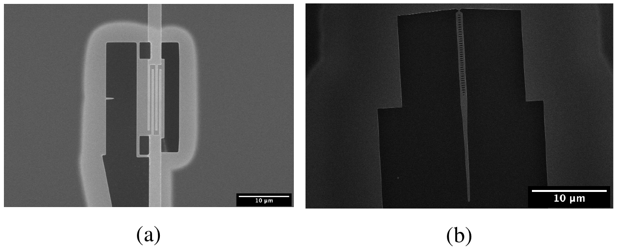
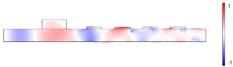
Several quantum transducers using thin-film lithium niobate have shown promising results Jiang et al. (2019); Shao et al. (2019); Jiang et al. (2020), due to the large values of the material’s piezoelectric tensor. However, these homogeneous approaches failed to achieve the high optomechanical coupling necessary for efficient transduction, as \ceLiNbO3 has a relatively small refractive index ( at 1550 nm). By incorporating a silicon cavity the optomechanical coupling of a thin-film lithium niobate device can be significantly increased. In our approach, the transducer is assembled by placing a one-dimensional silicon photonic crystal nanobeam on top of a suspended lithium niobate membrane patterned with electrodes used for piezoelectric coupling (see Fig. 2a). This hybrid structure supports mechanical modes that are distributed across both materials and that couple to both optical and microwave electromagnetic fields. The membrane resonator is made from X-cut lithium niobate and is designed to support GHz-frequency Lamb wave modes along the y-axis of the crystal, as shown in Figure 2b. Through finite-element simulations, we find A0-like modes (zeroth-order asymmetric Lamb wave), where the stress inside the silicon nanobeam closely resembles the stress distribution of its breathing mode Auld (1973) (cf. Fig. 2c). Higher piezoelectric coupling can be expected for S0-like modes, albeit with lower mechanical quality factor due to the geometry of our device. The mechanical modes of the membrane are excited by an array of equally spaced electrodes, known as an interdigital transducer (IDT). The pitch of the electrodes determines the frequency of the excited modes, while the number of fingers sets the bandwidth Campbell (1998). Using a large membrane with large number of IDT fingers will lead to higher coupling rates between mechanical modes and microwaves, but comes at the expense of reduced optomechanical coupling, as more effective mass is added to the mechanical mode. We design our electromechanical device with 2 finger pairs and dimensions of m, with a pitch of 1.5 m. From finite-element simulations, we expect an effective electromechanical coupling coefficient for our membrane design.
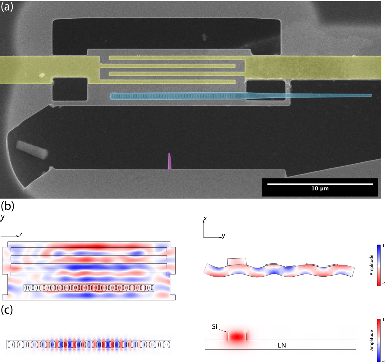
The silicon nanobeam optical cavity on top of the membrane is formed by a photonic crystal mirror at each end and a tapered defect region in the middle Chan et al. (2012), made out of 250 nm thick silicon. Finite-element simulations of the bare silicon photonic crystal cavity nanobeam show a fundamental resonance around 1565 nm with a quality factor exceeding . When the nanobeam is placed on top of the \ceLiNbO3 membrane its resonance is shifted to around 1595 nm (see Fig. 2c for details). We further calculate an optomechanical coupling rate of 24 kHz for an optimally positioned nanobeam.
We fabricate the lithium niobate devices using two electron-beam lithography steps. The first places electrodes on top of the membrane, and the second etches into the lithium niobate. The silicon nanobeam is fabricated in a single lithography step, with the photonic crystal cavity connected with single narrow bridge to the rest of the chip in order to be able to pick it up with the fiber during the transfer procedure (see the Supplementary Information for more details).
Slapping technique
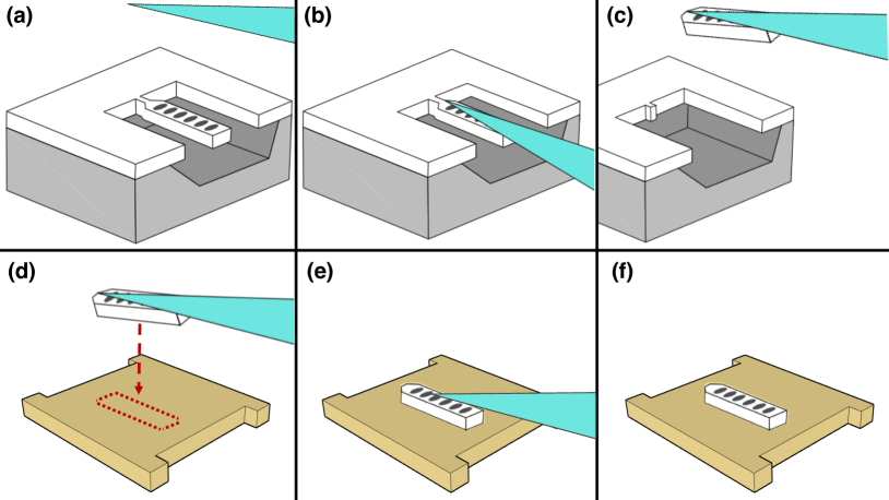
Our approach for making hybrid photonic integrated circuits is based on the pick-and-place method, where structures are removed from a “donor chip” made of a desired material and are transferred to a “device chip” made of a traditional photonic material. In the past, this transfer has been accomplished using polymer stamps Katsumi et al. (2018); Dibos et al. (2018), atomic force microscopy (AFM) tips Schell et al. (2011), or tungsten nanomanipulator probes Englund et al. (2010); Najafi et al. (2015); Mouradian et al. (2015); Zadeh et al. (2016); Kim et al. (2017); Wan et al. (2020). In contrast, we developed a new method using an optical fiber, which we refer to as slapping. One of the major advantages of our approach is that we can achieve high-precision positioning without sacrificing the ease of operation, because the silicon photonic devices can be directly and continuously measured during the transfer process.
Tapered optical fibers are commonly used to couple light into nanophotonic devices with high efficiency Gröblacher et al. (2013); Tiecke et al. (2015); Burek et al. (2017) and have also been used to rip away loosely connected photonic crystal cavities from the chip they were fabricated on Thompson et al. (2013); Magrini et al. (2018). Here, we extend this technique by placing the cavities onto a different substrate to create a hybrid photonic device. In our procedure (cf. Fig. S3), silicon photonic crystal cavity nanobeams are attached by a thin tether ( nm) on a donor chip. The chip is placed on a piezo-controlled motorized stage where it is viewed from above through a microscope objective using a charge-coupled device (CCD) camera. A tapered fiber is placed above the donor chip at an angle of a few degrees lower than horizontal, such that the tip is nearly parallel to the surface of the donor chip. The motorized stage is then used to touch the waveguide of a photonic crystal cavity using the tapered fiber and van der Waals forces cause the fiber to adhere to the silicon. At this point, the optical and mechanical spectra of the optomechanical nanobeam can be measured with a tunable laser and photodetector using the reflected light in the optical fiber. This measurement can be used to preselect photonic structures supporting high-quality optical and mechanical modes, increasing the yield of the final devices.
Once the fiber is stuck to the nanobeam, the stages can be moved back and forth by a few microns, until the tether brakes and the nanobeam is ripped away. The donor chip is then lowered away from the fiber, and the device chip is moved into its place. The fiber is brought close to the surface of the device chip such that the silicon nanobeam and lithium niobate membrane are in focus simultaneously. A rough alignment can be done using the camera and microscope. With the evanescent field of the cavity, the environment surrounding the nanobeam can be probed, and its position with respect to the substrate can be determined. To further improve the accuracy of this alignment we include a thin marker in the \ceLiNbO3 layer near the mechanical resonator (see Fig. 2a). By moving the nanobeam over this marker and monitoring the optical spectrum a sharp reduction in the quality factor of optical modes due to scattering in close proximity to the marker can be observed (cf. Fig. S4). Using this strategy, we are able to position the center of the optical cavity directly over the marker before transferring it to the mechanical resonator, which results in reliably placing our nanobeams with an accuracy of less than 100 nm, which is significantly better than what is possible with optical imaging methods. The angular alignment accuracy is typically . Additional reduction in the alignment error can easily be realized through contact sensing and monitoring of the mechanical resonance of the cavity.
Once positioned, the fiber is then lowered, until the nanobeam touches down onto the membrane. As the van der Waals force makes the nanobeam stick to the substrate more strongly than to the fiber, the fiber can be lifted away from the hybrid structure. A finalized device using this method is shown in Figure 2a. We note that this technique is not material-specific and only uses materials typically used in a laboratory capable of optical characterization.
Results
After assembly, we measure the microwave and optical reflection spectra of our devices, which were all patterned with the electrodes wired to large pads in a ground-signal-ground (GSG) configuration. We measure the signal in reflection using a coaxial radio frequency (RF) GSG probe and a vector network analyzer (VNA), and the signal is normalized to the open response of the probe.
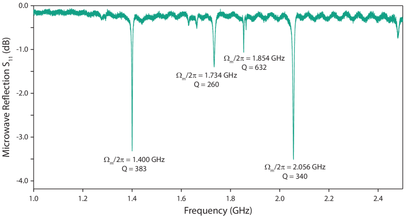
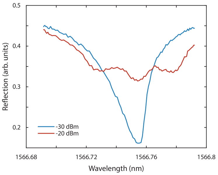
For our full procedure, we first characterize the lithium niobate resonator before slapping the silicon nanobeam by measuring the microwave reflection spectrum. Prominent dips in the reflection spectrum (see Fig. 3) indicate a power transfer into the mechanical modes of the device. After the slapping, the same measurement reveals that the resonances are slightly shifted, while the quality factors experience a modest decrease (Fig. 4b, red trace). We observe groups of modes spaced by approximately 330 MHz, which matches the free spectral range of the A0-like mechanical modes in our simulations. Optical spectroscopy of the hybrid device is performed using a tunable external-cavity diode laser. The reflection spectrum of the device shows two prominent resonances at 1588 and 1617 nm with a line width of 6.6 and 11.3 GHz, respectively (Fig. 4a).
We then proceed to measure microwave-to-optical transduction at room temperature. A microwave tone is swept over the device, exciting the mechanical supermodes of the hybrid nanobeam-and-membrane structure on resonance. At the same time, optical laser light detuned to the blue side of the cavity by 1.4 GHz is continuously pumped into the nanobeam, through an optical circulator and a tapered optical fiber. On resonance, the mechanical motion excited by the microwave signal will drive the optomechanical Stokes process and create a sideband resonant with the optical cavity. The optical intensity resulting from the beat note between the reflected cavity and pump photons can be measured by monitoring the light reflected from the cavity on a fast photodiode. Key parameters such as single-photon optomechanical coupling rate and microwave-to-optical efficiency can be extracted by comparing the response of the output of the fast photodetector to the microwave input. Using a VNA yields a transmission-type measurement of microwave-to-optical transduction (Fig. 4b, blue trace).
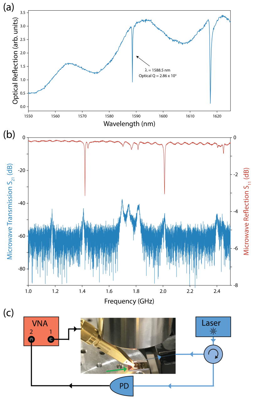
We select the mechanical mode at 1.7 GHz as our mechanical resonance as it has the highest value in our measurement. The input optical power sent into the cavity through the tapered fiber is W, while the overall received optical power at the photodiode is nW. Following Shao et al. (2019), the single-photon optomechanical coupling rate can be extracted from the in the sideband resolved regime, where we use for the impedance of the VNA ports and V/W as the responsivity of the photodiode. In our case the anti-Stokes sideband is not completely suppressed, leading to a slight under-estimation of . The microwave-to-optical transduction efficiency is the product of the single photon cooperativity , the intracavity photon number , and the microwave and optical external coupling efficiencies (, respectively):
| (1) |
We find kHz, which matches well with the simulated value of 13 kHz for a slightly nonoptimally placed nanobeam. While the large loss rates of the optical and mechanical resonators of GHz and MHz, respectively, keep this device out of the regime, the relatively high external coupling efficiencies result in a photon number conversion efficiency of at an optical power of W in the fiber. This result is on par with homogeneous state-of-the-art \ceLiNbO3 devices Shao et al. (2019); Jiang et al. (2020). On the one hand, while Ref. Shao et al. (2019) exhibits a large microwave-to-mechanics conversion , it suffers from a small optomechanical coupling kHz. On the other hand Ref. Jiang et al. (2019) utilizes small mode volume nanobeam cavities to achieve kHz but at the expense of low . Our platform combines the strengths of both, with kHz and . Compared to a recent AlN on Si design Mirhosseini et al. (2020), our device also exhibits a significantly higher piezoelectric coupling. Following Jiang et al. (2019), we estimate that the coupling of our device to a microwave LC resonator of the same impedance would yield about an order of magnitude higher coupling 2 MHz. An additional advantage of our design is the better thermal anchoring, resulting in a reduced susceptibility to optical absorption induced heating.
We have demonstrated a new approach for wavelength conversion that is on par with other recent state-of-the-art devices. We have done this by successfully integrating Silicon and LN into a single hybrid electro-optomechanical device using a new and simplified variation of the pick-and-place technique. Our work shows that placing can be done on a suspended membrane, while forming good mechanical contact. This confirms that this simple technique is relevant for fabricating optomechanical devices. As the material combination used in this work is superior for the optomechanical quantum transduction task than any other approach to date, additional adjustments to our platform can be used to significantly improve the performance of this new class of devices by several orders of magnitude. Coupling between microwave and mechanical modes can be increased by using an on-chip impedance matching circuit and switching to S0-like modes. In our \ceLiNbO3 membranes these modes suffered from small quality factors, which can be overcome by adjustments to the fabrication procedure, as similar designs have demonstrated S0-like modes with much larger factors Gong and Piazza (2013). This will enable us to use a smaller membrane (while preserving the piezo ), which will increase the optomechanical coupling rate. Further improvements in the fabrication will lead to higher optical quality factors and, hence, to a better overall efficiency, which has already been demonstrated in a similar structure Witmer et al. (2016). Our new slapping approach is also directly applicable to the precision positioning of photonic crystal cavities to spins in a substrate, such as for color centers in diamond Hausmann et al. (2013) and rare-earth ions Kindem et al. (2020); Raha et al. (2020). While a deterministic pick and place between nitrogen-vacancy centers and photonic crystal cavities has been demonstrated Englund et al. (2010), our approach using a tapered fiber for simultaneous high-efficiency readout and pick-and-place procedure with in situ alignment simplifies the assembly process significantly.
Acknowledgements.
We thank Robert Stockill, Moritz Forsch, and Roald van der Kolk for valuable discussions. This work is supported by the Foundation for Fundamental Research on Matter (FOM) Projectruimte Grant (16PR1054), the European Research Council (ERC StG Strong-Q, 676842), and by the Netherlands Organization for Scientific Research (NWO/OCW), as part of the Frontiers of Nanoscience program, as well as through Vidi (680-47-541/994) and Vrij Programma (680-92-18-04) grants. B.H. acknowledges funding from the European Union under a Marie Skłodowska-Curie COFUND fellowship.References
- Benson (2011) O. Benson, Nature 480, 193 (2011).
- Marpaung et al. (2019) D. Marpaung, J. Yao, and J. Capmany, Nature Photon. 13, 80 (2019).
- Elshaari et al. (2020) A. W. Elshaari, W. Pernice, K. Srinivasan, O. Benson, and V. Zwiller, Nature Photon. 14, 285 (2020).
- Chu and Gröblacher (2020) Y. Chu and S. Gröblacher, Appl. Phys. Lett. 117, 150503 (2020).
- Kim et al. (2017) J.-H. Kim, S. Aghaeimeibodi, C. J. K. Richardson, R. P. Leavitt, D. Englund, and E. Waks, Nano Lett. 17, 7394 (2017).
- Liu et al. (2011) M. Liu, X. Yin, E. Ulin-Avila, B. Geng, T. Zentgraf, L. Ju, F. Wang, and X. Zhang, Nature 474, 64 (2011).
- Thomson et al. (2016) D. Thomson, A. Zilkie, J. E. Bowers, T. Komljenovic, G. T. Reed, L. Vivien, D. Marris-Morini, E. Cassan, L. Virot, J.-M. Fédéli, J.-M. Hartmann, J. H. Schmid, D.-X. Xu, F. Boeuf, P. O’Brien, G. Z. Mashanovich, and M. Nedeljkovic, J. Opt. 18, 073003 (2016).
- Wendin (2017) G. Wendin, Rep. Prog. Phys. 80, 106001 (2017).
- Magnard et al. (2020) P. Magnard, S. Storz, P. Kurpiers, J. Schär, F. Marxer, J. Lütolf, J.-C. Besse, M. Gabureac, K. Reuer, A. Akin, B. Royer, A. Blais, and A. Wallraff, Phys. Rev. Lett. 125, 260502 (2020).
- Lambert et al. (2020) N. J. Lambert, A. Rueda, F. Sedlmeir, and H. G. L. Schwefel, Adv. Quantum Technol. 3, 1900077 (2020).
- Lauk et al. (2020) N. Lauk, N. Sinclair, S. Barzanjeh, J. P. Covey, M. Saffman, M. Spiropulu, and C. Simon, Quantum Sci. Technol. 5, 20501 (2020).
- Kimble (2008) H. J. Kimble, Nature 453, 1023 (2008).
- Wehner et al. (2018) S. Wehner, D. Elkouss, and R. Hanson, Science 362, eaam9288 (2018).
- Tian and Wang (2010) L. Tian and H. Wang, Phys. Rev. A 82, 053806 (2010).
- Bochmann et al. (2013) J. Bochmann, A. Vainsencher, D. D. Awschalom, and A. N. Cleland, Nature Phys. 9, 712 (2013).
- Bagci et al. (2014) T. Bagci, A. Simonsen, S. Schmid, L. G. Villanueva, E. Zeuthen, J. Appel, J. Taylor, A. Sørensen, K. Usami, A. Schliesser, and E. Polzik, Nature 507, 81 (2014).
- Balram et al. (2016) K. C. Balram, M. I. Davanço, J. D. Song, and K. Srinivasan, Nature Photon. 10, 346 (2016).
- Higginbotham et al. (2018) A. P. Higginbotham, P. S. Burns, M. D. Urmey, R. W. Peterson, N. S. Kampel, B. M. Brubaker, G. Smith, K. W. Lehnert, and C. A. Regal, Nature Phys. 14, 1038 (2018).
- Shao et al. (2019) L. Shao, M. Yu, S. Maity, N. Sinclair, L. Zheng, C. Chia, A. Shams-Ansari, C. Wang, M. Zhang, K. Lai, and M. Lončar, Optica 6, 1498 (2019).
- Jiang et al. (2019) W. Jiang, R. N. Patel, F. M. Mayor, T. P. McKenna, P. Arrangoiz-Arriola, C. J. Sarabalis, J. D. Witmer, R. V. Laer, and A. H. Safavi-Naeini, Optica 6, 845 (2019).
- Forsch et al. (2020) M. Forsch, R. Stockill, A. Wallucks, I. Marinković, C. Gärtner, R. A. Norte, F. van Otten, A. Fiore, K. Srinivasan, and S. Gröblacher, Nature Phys. 16, 69 (2020).
- Han et al. (2020) X. Han, W. Fu, C. Zhong, C.-L. Zou, Y. Xu, A. A. Sayem, M. Xu, S. Wang, R. Cheng, L. Jiang, and H. X. Tang, Nature Commun. 11, 3237 (2020).
- Jiang et al. (2020) W. Jiang, C. J. Sarabalis, Y. D. Dahmani, R. N. Patel, F. M. Mayor, T. P. McKenna, R. Van Laer, and A. H. Safavi-Naeini, Nature Commun. 11, 1166 (2020).
- Arnold et al. (2020) G. Arnold, M. Wulf, S. Barzanjeh, E. S. Redchenko, A. Rueda, W. J. Hease, F. Hassani, and J. M. Fink, Nature Commun. 11, 4460 (2020).
- Mirhosseini et al. (2020) M. Mirhosseini, A. Sipahigil, M. Kalaee, and O. Painter, Nature 588, 599 (2020).
- Aspelmeyer et al. (2014) M. Aspelmeyer, T. J. Kippenberg, and F. Marquardt, Rev. Mod. Phys. 86, 1391 (2014).
- Wu et al. (2020) M. Wu, E. Zeuthen, K. C. Balram, and K. Srinivasan, Phys. Rev. Applied 13, 014027 (2020).
- Chan et al. (2011) J. Chan, T. P. M. Alegre, A. H. Safavi-Naeini, J. T. Hill, A. Krause, S. Gröblacher, M. Aspelmeyer, and O. Painter, Nature 478, 89 (2011).
- Riedinger et al. (2016) R. Riedinger, S. Hong, R. A. Norte, J. A. Slater, J. Shang, A. G. Krause, V. Anant, M. Aspelmeyer, and S. Gröblacher, Nature 530, 313 (2016).
- Wallucks et al. (2020) A. Wallucks, I. Marinković, B. Hensen, R. Stockill, and S. Gröblacher, Nature Phys. 16, 772 (2020).
- Chu et al. (2017) Y. Chu, P. Kharel, W. H. Renninger, L. D. Burkhart, L. Frunzio, P. T. Rakich, and R. J. Schoelkopf, Science 358, 199 (2017).
- Satzinger et al. (2018) K. J. Satzinger, Y. P. Zhong, H.-S. Chang, G. A. Peairs, A. Bienfait, M.-H. Chou, A. Y. Cleland, C. R. Conner, E. Dumur, J. Grebel, I. Gutierrez, B. H. November, R. G. Povey, S. J. Whiteley, D. D. Awschalom, D. I. Schuster, and A. N. Cleland, Nature 563, 661 (2018).
- Arrangoiz-Arriola et al. (2019) P. Arrangoiz-Arriola, E. A. Wollack, Z. Wang, M. Pechal, W. Jiang, T. P. McKenna, J. D. Witmer, R. V. Laer, and A. H. Safavi-Naeini, Nature 571, 537 (2019).
- Safavi-Naeini et al. (2019) A. H. Safavi-Naeini, D. V. Thourhout, R. Baets, and R. V. Laer, Optica 6, 213 (2019).
- Auld (1973) B. A. Auld, Acoustic fields and waves in solids (Wiley Interscience Publications, 1973).
- Campbell (1998) C. Campbell, Surface Acoustic Wave Devices for Mobile and Wireless Communications, Four-Volume Set (Academic press, 1998).
- Chan et al. (2012) J. Chan, A. H. Safavi-Naeini, J. T. Hill, S. Meenehan, and O. Painter, App. Phys. Lett. 101, 081115 (2012).
- Katsumi et al. (2018) R. Katsumi, Y. Ota, M. Kakuda, S. Iwamoto, and Y. Arakawa, Optica 5, 691 (2018).
- Dibos et al. (2018) A. M. Dibos, M. Raha, C. M. Phenicie, and J. D. Thompson, Phys. Rev. Lett. 120, 243601 (2018).
- Schell et al. (2011) A. W. Schell, G. Kewes, T. Schröder, J. Wolters, T. Aichele, and O. Benson, Rev. Sci. Instr. 82, 073709 (2011).
- Englund et al. (2010) D. Englund, B. Shields, K. Rivoire, F. Hatami, J. Vučković, H. Park, and M. D. Lukin, Nano Lett. 10, 3922 (2010).
- Najafi et al. (2015) F. Najafi, J. Mower, N. C. Harris, F. Bellei, A. Dane, C. Lee, X. Hu, P. Kharel, F. Marsili, S. Assefa, K. K. Berggren, and D. Englund, Nature Commun. 6, 5873 (2015).
- Mouradian et al. (2015) S. L. Mouradian, T. Schröder, C. B. Poitras, L. Li, J. Goldstein, E. H. Chen, M. Walsh, J. Cardenas, M. L. Markham, D. J. Twitchen, M. Lipson, and D. Englund, Phys. Rev. X 5, 031009 (2015).
- Zadeh et al. (2016) I. E. Zadeh, A. W. Elshaari, K. D. Jöns, A. Fognini, D. Dalacu, P. J. Poole, M. E. Reimer, and V. Zwiller, Nano Lett. 16, 2289 (2016).
- Wan et al. (2020) N. H. Wan, T.-J. Lu, K. C. Chen, M. P. Walsh, M. E. Trusheim, L. D. Santis, E. A. Bersin, I. B. Harris, S. L. Mouradian, I. R. Christen, E. S. Bielejec, and D. Englund, Nature 583, 226 (2020).
- Gröblacher et al. (2013) S. Gröblacher, J. T. Hill, A. H. Safavi-Naeini, J. Chan, and O. Painter, Appl. Phys. Lett., 103, 181104 (2013).
- Tiecke et al. (2015) T. G. Tiecke, K. P. Nayak, J. D. Thompson, T. Peyronel, N. P. de Leon, V. Vuletić, and M. D. Lukin, Optica 2, 70 (2015).
- Burek et al. (2017) M. J. Burek, C. Meuwly, R. E. Evans, M. K. Bhaskar, A. Sipahigil, S. Meesala, B. Machielse, D. D. Sukachev, C. T. Nguyen, J. L. Pacheco, E. Bielejec, M. D. Lukin, and M. Lončar, Phys. Rev. Appl. 8, 024026 (2017).
- Thompson et al. (2013) J. D. Thompson, T. G. Tiecke, N. P. de Leon, J. Feist, A. V. Akimov, M. Gullans, A. S. Zibrov, V. Vuletić, and M. D. Lukin, Science 340, 1202 (2013).
- Magrini et al. (2018) L. Magrini, R. A. Norte, R. Riedinger, I. Marinković, D. Grass, U. Delić, S. Gröblacher, S. Hong, and M. Aspelmeyer, Optica 5, 1597 (2018).
- Gong and Piazza (2013) S. Gong and G. Piazza, IEEE Trans. Microw. Theory Tech. 61, 403 (2013).
- Witmer et al. (2016) J. D. Witmer, J. T. Hill, and A. H. Safavi-Naeini, Opt. Express 24, 5876 (2016).
- Hausmann et al. (2013) B. J. M. Hausmann, B. J. Shields, Q. Quan, Y. Chu, N. P. de Leon, R. Evans, M. J. Burek, A. S. Zibrov, M. Markham, D. J. Twitchen, H. Park, M. D. Lukin, and M. Lonc̆ar, Nano Lett. 13, 5791 (2013).
- Kindem et al. (2020) J. M. Kindem, A. Ruskuc, J. G. Bartholomew, J. Rochman, Y. Q. Huan, and A. Faraon, Nature 580, 201 (2020).
- Raha et al. (2020) M. Raha, S. Chen, C. M. Phenicie, S. Ourari, A. M. Dibos, and J. D. Thompson, Nature Commun. 11, 1 (2020).
- Marinković (2019) I. Marinković, Optomechanical Devices in the Quantum Regime, Ph.D. thesis, Delft University of Technology (2019).
- Wang et al. (2013) R. Wang, S. A. Bhave, and K. Bhattacharjee, in Proceedings of the IEEE International Conference on Micro Electro Mechanical Systems (MEMS) (2013) pp. 165–168.
- Wang et al. (2014) C. Wang, M. J. Burek, Z. Lin, H. A. Atikian, V. Venkataraman, I.-C. Huang, P. Stark, and M. Lončar, Opt. Express 22, 30924 (2014).
- Arrangoiz-Arriola et al. (2018) P. Arrangoiz-Arriola, E. A. Wollack, M. Pechal, J. D. Witmer, J. T. Hill, and A. H. Safavi-Naeini, Phys. Rev. X 8, 031007 (2018).
- Itano et al. (1993) M. Itano, F. W. Kern, M. Miyashita, and T. Ohmi, IEEE Trans. Semicond. Manuf. 6, 258 (1993).
- Cai et al. (2019) L. Cai, A. Mahmoud, and G. Piazza, Opt. Express 27, 9794 (2019).
Supplementary Information
.1 Fabrication
We begin with a Lithium Niobate on Silicon (LNOS) mm chip, consisting of a 340 nm layer of X-cut, single crystal lithium niobate doped with 5 mol \ceMgO bonded to a 500 m thick silicon substrate. Electrodes are defined by first patterning a 280 nm thick coating of electron beam resist and then evaporating an adhesion layer consisting 5 nm of chromium and 15 nm of platinum under a 40 nm layer of gold. The evaporation step is followed by lift-off, where the chip is placed in a beaker of anisole heated to C and set in an ultrasonic bath for five minutes. Next, the second electron beam lithography step defines the shape of the thin film resonators in a thick 550 nm coating of CSAR62.13 resist. The exposed lithium niobate is etched through by a large cross-sectional beam of argon ions incident at a 90-degree angle to the surface of the chip. This process etches through the lithium niobate membrane and results in a sidewall angle of . The devices are released using a dry \ceSF6 reactive ion etch which isotropically etches the silicon through the holes in the lithium niobate film. The resist is not stripped until after the underetching step in order to prevent contamination of the etcher. At this point, resist removal is achieved by ashing in oxygen plasma. Finally, we employ an inorganic cleaning step to remove lithium niobate redeposited during the physical etching. We prepare a mixture similar to RCA-1, a 2:2:1 ratio of \ceNH4OH [] : \ceH2O2 [] : \ceH2O. The mixture is heated to C and mixed with a stir bar for 5 minutes before our samples are placed in for another 5 minutes. A fabricated device is shown in Fig. S1a. The silicon nanobeam fabrication is described in detail in Marinković (2019), with the liquid HF undercut being replaced with vapor HF. A fabricated nanobeam device is shown in Fig. S1b.
.2 Redeposition of Lithium Niobate
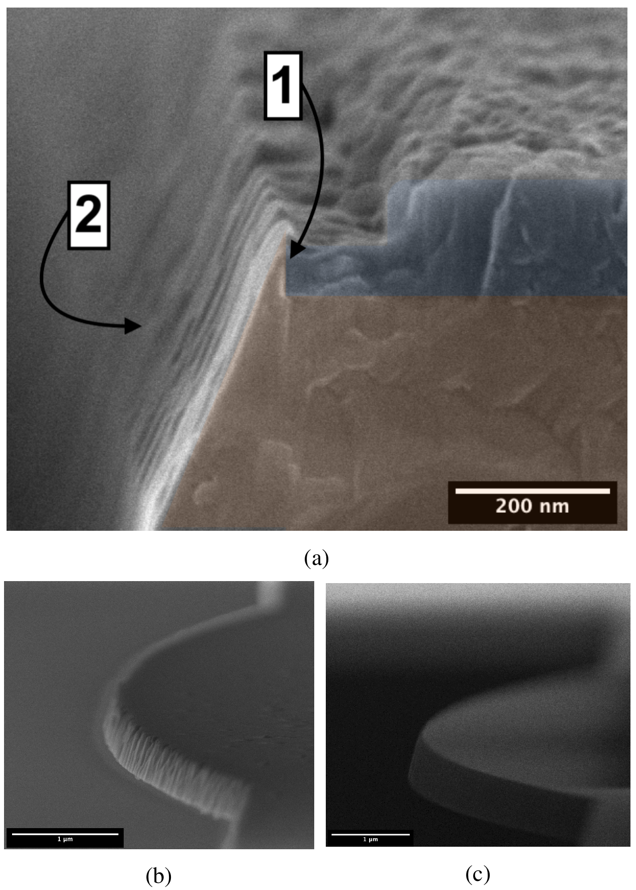
Despite being a widely used material across multiple industries for decades, the nanofabrication of lithium niobate is considered difficult. There is no known chemical etch for lithium niobate that produces desirable devices with acceptable sidewalls and low surface roughness without unwanted contamination. This leaves as the only viable alternative physical etching. Inspired by Refs. Wang et al. (2013, 2014); Arrangoiz-Arriola et al. (2018), we process our lithium niobate using argon ion beam etching (also called ion milling) in an inductively coupled plasma etcher. However, ion milling lithium niobate causes amorphous \ceLiNbO3 redeposition, creating unwanted features and increasing sidewall roughness as seen in Figs. S2a and S2b. We mitigate this problem first by optimizing the plasma etching parameters to minimize redeposition and then by chemically cleaning our sample. The results are shown in Fig. S2c. The chemical cleaning step is based on RCA-1, which is typically used on silicon devices Itano et al. (1993) and found to also be effective on lithium niobate Cai et al. (2019).
.3 Slapping Procedure
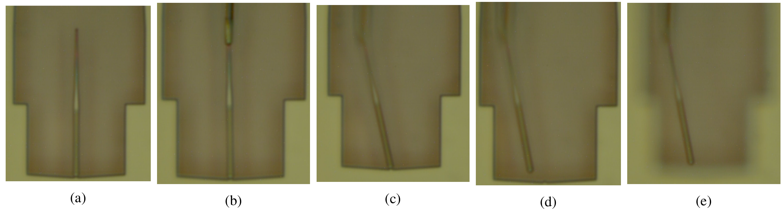
The slapping technique consists of first picking up and then slapping down a structure from a donor chip onto a device chip. The pick-up procedure begins by placing a silicon donor chip under a microscope and locating a photonic crystal cavity nanobeam (Fig. S3a). In this image, the device is connected to the chip by a thin tether at the bottom (see SEM in Fig. S1b). Next, a tapered optical fiber is lowered until the device and the tip of the fiber are simultaneously in focus. The tapered fiber is then placed on the tapered waveguide of the nanobeam (Fig. S3b). It is easy to distinguish when the fiber is touching the nanobeam, as the fiber changes color on contact. At this stage, the optical and mechanical spectra of the nanobeam device can be measured in order to confirm that it is functioning as intended. When the fiber is moved to the left or the right, the nanobeam adheres and pivots around the tether (Fig. S3c). We find that sweeping the fiber left and right by a few microns reliably breaks a 50-100 nm thick tether. Once the tether is broken, the nanobeam can be pulled away from the donor chip (Fig. S3d) and finally be lifted away (Fig. S3e).
Next, after picking up the nanobeam, it can be placed back down wherever desired. Slapping the nanobeam only requires that the structure sticks better to the new substrate than it does to the tapered fiber tip. This is usually true for any material, as the nanobeam is picked up in such a way that it contacts only a small fraction of the nanobeam’s surface area. When the nanobeam is slapped down, its entire bottom surface touches the substrate and thus it adheres. We found that once slapped, the structures’ position can be further adjusted by pushing them across the substrate with the tapered fiber after slapping.
.4 Increasing Slapping Accuracy with In-Situ Optical Sensing
The accuracy of slapping an arbitrary structure is in principle limited by the optical diffraction limit and practically by operator error. However, in our approach we are picking up optical cavities with an optical fiber. This allows us to significantly improve the accurate placement by measuring the photonic crystal cavity during the slapping procedure.
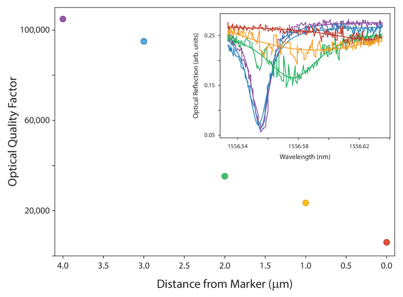
In order to demonstrate and characterize the in-situ alignment procedure of the position of the cavity with respect to a feature on a device chip, we monitor the resonance as we approach a silicon marker. The marker is simply a 270-nm thick silicon cantilever, similar to the lithium niobate marker visible in the bottom of Fig. 2b. In order to sense the marker, the nanobeam is placed a few hundred nanometers above the device chip while the optical resonance is measured on reflection using the tapered fiber. Scattering drastically reduces the quality factor of the optical cavity when the marker is near the defect region of the photonic crystal. In addition, the resonances are slightly redshifted close to the marker (see Fig. S4). Both effects are clear, as the redshift and the linewidth of the fundamental optical mode increase with proximity to the marker. By fitting the data to find the position of maximum absorption, we can locate the center of the photonic crystal cavity directly over the on-chip marker. Using this technique, we are able to position a nanobeam with an accuracy of better than 100 nm, well under the optical diffraction limit (100s of nanometers in this case).
.5 Photonic Crystal Design
The cavity is formed by two photonic crystal mirrors at each end and a tapered region in the middle, designed and fabricated according to Witmer et al. (2016). The unit cell periodicity of the mirror is nm and hole axes are nm and nm, while the width of the nanobeam is nm and the thickness of the silicon layer is nm. The lattice spacing is quadratically tapered to a value nm and nm in the central defect region. Through the simulation of the optomechanical coupling rate of various mechanical modes to the photonic cavity, we confirm that the coupling inside the lithium niobate is small and hence can be neglected, as most of the optical mode is contained inside of the silicon. The relatively low quality factor of the fabricated cavities can be attributed to poor etching of the silicon.
.6 of S0 mode
We calculate the optomechanical coupling rate for S0-like modes of our hybrid device (Fig S5), as these modes have higher piezoelectric coupling. We obtain kHz for a GHz mode.
.7 Estimation of
Here we like to sketch how we estimate from our experimental data. Light in the photonic cavity can be decomposed into three fields: the pump and the two optical sidebands shifted from the pump by the RF drive frequency. Expressions for the amplitudes of these waves (, and ) are derived in Shao et al. (2019):
where is the detuning of the laser with respect to the cavity. , with and being the frequency and power of the microwave drive of the mechanical resonator, respectively, and . Light coming out of the cavity is then given by:
After propagating to the detector with an efficiency , we detect the signal at the mechanical frequency with an amplitude . We then calculate the power that the VNA receives as , and finally obtain . Using this relationship between and we can then numerically calculate .
.8 of a Hybrid Device
We have characterize another device with higher mechanical frequency and slightly smaller optical linewidth. This enables us to clearly see the modification of optical reflection spectrum due the presence of RF drive on the IDTs (see Fig. S6), as done in Ref. Shao et al. (2019). This makes the resonance frequency of the cavity to oscillate with respect to the laser at the drive frequency. In the cavity’s frame of reference the laser frequency is modulated, giving rise to sidebands at the RF drive frequency. We use the formula given in Shao et al. (2019)
| (S1) |
to estimate the mV of our device.