Observation of Josephson-like tunneling junction characteristics
and positive magnetoresistance in Oxygen deficient Nickelate films of
Abstract
Nickelate films have recently attracted broad attention due to the observation of superconductivity in the infinite layer phase of (obtained by reducing Sr doped films) and their similarity to the cuprates high temperature superconductors. Here we report on the observation of a new type of transport in oxygen poor films. At high temperatures, variable range hopping is observed while at low temperatures a novel tunneling behavior is found where Josephson-like tunneling junction characteristic with serial resistance is revealed. We attribute this phenomenon to coupling between superconductive (S) surfaces of the grains in our Oxygen poor films via the insulating (I) grain boundaries, which yields SIS junctions in series with the normal (N) resistance of the grains themselves. The similarity of the observed conductance spectra to tunneling junction characteristic with Josephson-like current is striking, and seems to support the existence of superconductivity in our samples.
pacs:
74.50.Br, 74.78.Aw, 73.50.Ah, 73.43.QtI Introduction
The recent discovery of superconductivity in thin films Hwang has brought up research of the Nickelates to the front of condense matter physics MikeNorman . These materials are interesting since they are similar in structure and electronic properties to the cuprate family which is well known for its high temperature superconductivity. It is expected that understanding the similarities and differences between these two families of materials will complement each other and illuminate the mechanism of superconductivity in the cuprates which is still under debate. The phase diagram of the films and more of their basic properties are given in LiHwangPRL . Superconductivity was observed also in thin films OsadaHwang but in both this study and Ref. Hwang the films thickness ranged between 5 and 12 nm only. Thicker films of this kind showed absence of superconductivity in bulk form LiWen ; Zhou and raised the question whether the observed superconductivity in the few nm thick films is an interface effect originating in strains with the substrate. The way in which the thin films were prepared involved laser deposition of the perovskite films first, which were then reduced by a chemical annealing process with that changed them to the superconductive infinite layer phase Hwang . Similar films were fabricated successfully by other groups using the same process Ariando ; GuWen ; YingWen , but it was clear from the beginning that this reduction process is not just simple extraction of oxygen from the films since it involved also a major change of their structural phase. In view of this, a few groups tried to reproduced Ref. Hwang results by physical extraction of oxygen from the precursor films by annealing at elevated temperatures under vacuum or with low oxygen pressure. Unfortunately, this led to even more insulating films and no change of phase to the superconductive infinite layer one was obtained LiWen ; Zhou . In the present study, we also used physical reduction of the precursor insulating films of and investigated their properties. In particular, annealing under 10 mTorr oxygen increased the films resistivity at low temperatures by two order of magnitudes but didn’t change their structural phase. These films showed variable range hopping (VRH) transport in 2D versus temperature with deviation due to tunneling conductance below about 4 K. In view of our results, we make the conjecture that this deviation toward increasing resistance originates in gap opening and tunneling between superconductive (S) surfaces of the grains in the films via the insulating (I) grain boundaries. Thus accordingly, our films can be visualized as comprised of a network of SIS tunneling junctions connected in series with additional serial resistance of the normal (N) grains themselves.
II Experiment
Preparation of the target and films
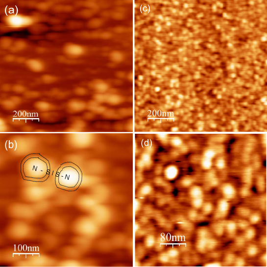
Standard pulsed laser ablation deposition from ceramic target was used. The target was prepared by mixing stoichiometric amounts of , and , then baking, grinding and weighing in 5 steps at 9300C/12h, 10500C/40h, 12200C/24h, 12500C/24h and finally pressing and sintering a pellet at 13500C/12h. Most of the weight loss was after the first step where the powder lost most of its , but even in the last step a small weight lost was still found indicating that was still being removed from the target. For obtaining high quality films of the cuprates it was essential to have Carbon free targets and we believe it is just as important here. For the deposition of the thin films we used third harmonic Nd-YAG laser pulses at 355 nm with 1.5 J/cm2 on the target. The area substrates of (100) (STO) wafers were clamped to a heater block and deposition was carried out at four different substrate temperatures of 450, 600, 650 and 700 0C (the corresponding heater block temperatures were about 150 0C higher). Deposition was done under 100 mTorr flow of Oxygen and the deposition rate was about 0.07 nm per pulse. After deposition, the heater was turned off and cooling was under the same Oyxgen pressure flow. The resulting films were shiny black, well crystallized and very smooth as can be seen by the AFM images of Fig. 1 for the two films deposited at 600 and 6500C.
X-ray characterization of the films
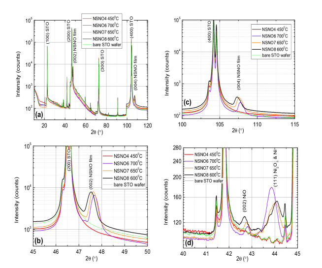
Fig. 2 exhibits X-ray diffraction results of our as deposited films on (100) wafers under various substrate temperatures. It shows that the perovskite phase was obtained, except for the too low 4500C deposition which can be considered as background for the other data. We focus on two regions near the most prominent (002) and (004) peaks of the films as depicted in (b) and (c), respectively. The peak at (001) was weak and the one at (003) was absent. The measured 2 width at half maximum (FWHM) of the un-split (004) peaks of the different films is about 0.780 which is approximately equal to twice the split of the (400) STO peaks (0.360) resulting from the and Copper lines as seen in (c). For the (002) peak of the films as seen in (b), the measured width is 0.330 which is about three times the split of the (200) peak of STO (0.120). Comparing our data to that of Li et al Hwang reveal two important differences: One is the much larger width of the (002) peak in Ref. Hwang of about 10 FWHM as compared to ours of 0.330 FWHM even though ours includes the Copper line contribution. This indicates a much better crystallization of the films in the present study. It might still have been advantageous for Li et al to have this poorer crystallization since the objective was to obtain the infinite layer phase of for which the chemical reduction of poorer precursor was easier. A second difference is that the (001) and (002) peaks in Hwang were of comparable intensity while in our data the (001) peak is much weaker than the (002) one. Li et al also say that their (003) film peak is not visible owing to its low intensity which is also what we observed. Generally however, the intensity of the even peaks in a perovskite [(002) and (004)] is much higher than that of the odd peaks [(001) and (003)], like for instance in STO. Thus the robust (001) peak in Ref. Hwang is puzzling, but it might be associated with the much thinner strained films involved.
Another relevant issue is the small minority phases observed in Fig. 2 (d). These were identified as due to various Nickel oxides , of which we marked in (d) , and , but other mixed stoichiometries are also possible as the broad, unresolved multiple peaks near 440 indicates. All these peaks are shifted to lower angles by 0.5-0.70 compared to their location in powder diffractometry due to compressive strains with the STO substrate and the films. For instance, the lattice constant of cubic (0.4177 nm) is larger than that of the STO wafer (0.3904 nm) and the present NSNO8 film (0.3838 nm), thus compressive epitaxial strain in the a-b plane of the elongates its c-axis to 0.4236 nm and lowers the diffraction angle to where it appears in (d). To estimate the percentage of these minority phases in our films as seen in (d), we compare their peak heights (between 15 and 75 counts) to that of the (002) peak of NSNO8 in (b) (5900 counts), and obtain about 0.3-1.3%. Generally, one would ignore such small quantities of secondary minority phases, but since it is most likely that these phases reside on the surface of the films and in their grain boundaries (by zone refining), they are very relevant for the present study where the transport in our films is strongly affected by these regions. In particular, as we shall see in the following, the magnetic properties of these phases Madhu ; Liu ; Luo ; Dey could play a role in explaining our transport results.
Physical reduction of the films
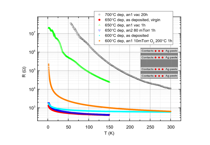
As mentioned before, physical reduction of our films was carried out rather than the chemical reduction with used previously Hwang ; LiHwangPRL ; OsadaHwang ; Ariando ; GuWen ; YingWen . Three annealing procedures were used all at the same 2000C temperature. The first two under vacuum for 24 h and for 1 h, and the third one under 10 mTorr of Oxygen flow for 1 h and cooling under the same pressure. The first two annealing processes yielded very resistive films with several tens of M resistance. The third annealing process was chosen since deposition (at 6000C) by Zhou et al Zhou at the same Oxygen pressure didn’t yield the phase at all. For our NSNO8 film deposited also at 6000C, the low annealing temperature preserved the phase, but increased the film resistance at low temperatures by two orders of magnitude. We note also that all annealing processes were reversible, and once reannealed at 2000C and 100 mTorr Oxygen pressure the films returned almost to their original as deposited state. Plots of some resistance versus temperature results of the various films with and without annealing is given in Fig. 3.
The measuring systems and contacts
Two measuring systems were used in the present study. One a physical properties measurement system with a closed cycle refrigerator and a magnet of up to 14 T (PPMS & DynaCool of Quantum Design) and the other a home made transport measurements probe inside a cryogenic dewar with liquid He and a magnet of up to 8 T (Teslatron of Oxford Inst.). The probe of the latter system had an array of 410 gold-coated spring loaded tips pressed onto the films for a 10 four probe measurements on different location ( for to 10) of the wafer. Due to a problem with this probe, the high temperature readings were unreliable and therefore the corresponding data in Fig. 3 was truncated above 150 K. Nevertheless, the Teslatron system was much more versatile and controllable than the PPMS in IVC and conductance spectra measurements at low temperatures and therefore all these measurements were carried out on it. To minimize the contact resistance four parallel silver paste bands for the four probe measurements were applied to the films as shown in the inset to Fig. 3. In the PPMS four contacts were first wire-bonded to the film and then the Ag paste bands were applied to overlap each bonding spot and extend the contacts along the wafer. In the Teslatron probe, 10 measurements were done simultaneously on 10 different areas of the film in such a way that the spring loaded contact tips were touching each band for every set of four contacts (three such sets are marked by red circles in the inset to Fig. 3).
III Results and discussion
Variable range hopping in 2D
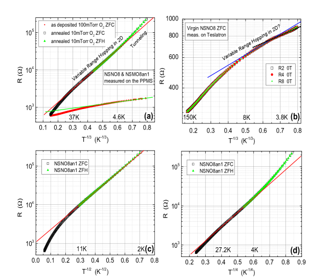
As can be seen from Figs. 2 and 3, all three films are c-axis oriented, have the perovskite phase and show insulating behavior at low temperatures, more so when reduced to extract Oxygen from them. As no metallic behavior is observed in the R vs T results of Fig. 3, one has to conclude that the dominant part of the resistance is determined by the insulating grain boundaries. Since the NSNO8 film deposited at 6000C still had the perovskite phase as reported also by other groups Hwang ; Ariando ; GuWen , we chose to focus on it. Moreover, its annealing under 10 mTorr flow at 2000C for 1 hour yielded a convenient resistance range at low temperatures for IVC and conductance measurements. To find out what is the conductance mechanism of the insulating as deposited film and the reduced film, we plot in Fig. 4 (a) and (b) their resistance on a log-scale versus . The expected behavior on such a plot should be linear if variable range hopping (VRH) in 2D occurs Shklovskii ; Fisher . As one can see in Fig. 4 (a), this is actually so over one order of magnitude of resistance change for the reduced film, but the linearity range hardly covers a factor of two change in resistance for the as deposited film. In addition, the resistance data of the latter as measured in the PPMS was quite noisy and allowed for a straight line to be drawn through the data as seen in (a). Measurement on three different areas (R2, R4 and R8) of the same film on the Teslatron system was much less noisy (see Fig. 4 (b)), and one can see that the linear range in R in this case is even smaller (about 100 only), if at all. For comparison, we also tried to fit the NSNO8an1 resistance data to two additional VRH models, one of Coulomb coupling between conducting grains (log R vs ) as seen in (c), and the other of VRH in 3D (log R vs ) as depicted in (d). Linearity is observed in all models, but its temperature range is largest in (a) (37 to 4.6 K). The corresponding linearity range in (c) is 2-11 K, and in (d) 4-27.2 K. If the resistance range where linearity is observed is the important factor in determining which of the VRH model applies, then (c) is the most likely model. However, we believe that the upturn from linear behavior below about 4 K in the annealed film in Fig. 4 (a) and (d) is a real effect which indicates decreased conductance with decreasing temperature. As we shall see in the following, this is due to tunneling conductance and gap opening which lower the number of states to which the electrons can tunnel and therefore increase the film resistance compared to the VRH behavior.
Tunneling conductance in the NSNO8 films
Fig. 5 depicts typical conductance spectra at various temperatures on two different areas of the as deposited NSNO8 and the oxygen deficient NSNO8an1 films. As we have seen before in Fig. 4 (a), transport in the annealed NSNO8an1 film occurs via VRH in 2D in an intermediate temperature range, while at low temperatures we proposed that tunneling takes over. Fig. 5 actually shows this tunneling conductance behavior with a narrow gap and a wide gap. The narrow gap is well developed at 1.8 K and up to at least 5 K in both films. This gap fills-in with increasing temperature and disappears above about 20 K, which is very much like a superconductive gap behavior. However, Fig. 5 (a) shows the conductance of the as deposited film is insensitive to a magnetic field of 1 T at 1.8 K. The same is true for the annealed film under 4 T field (will be shown later). These findings are at odds with the existence of conventional spin-singlet superconductivity in our films, where suppression of the zero bias conductance under field is expected. The observed insensitivity to magnetic field therefore might indicate that unconventional superconductivity such as same-spin triplet superconductivity is at the origin of the observed gap in Fig. 5. The presence of a small amount of ferromagnetic in our films as seen in Fig. 2 (d) and also found by He et al HeWen in similar polycrystalline , could facilitate triplet superconductivity as found in other ferromagnetic-superconductor systems Keizer ; Yoavtriplet . To further investigate these issues we present in Fig. 6 additional current versus voltage curves (IVCs) and conductance spectra of NSNO8an1 on different areas of the film (R8 but also on R2) which are more reminiscent of superconductive tunneling junctions with serial resistance.
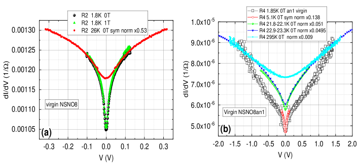
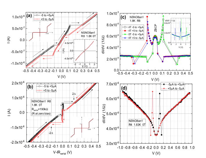
Fig. 6 (a) shows a full cycle IVCs at 1.8 K and zero field on the R8 area of the NSNO8an1 film under current bias. Increasing current and decreasing current are marked by different colors and the arrows indicate the direcion in which the IVC cycle develops. A zoom out to the full current scale is given in the right inset. The prominent features in Fig. 6 (a) are the asymmetric voltage jumps, which look symmetric only when the full current cycle is drawn. Comparing the present IVC characteristic to that of a typical Josephson tunnel junction (JTJ) as depicted schematically in the left inset, one finds a striking similarity except for the fact that the Josephson-like current of the central segment of the IVC (the supercurrent part) is obviously affected by a serial resistance . When the voltage drop on this resistance is subtracted from the measured voltage, the resulting I vs which is shown in Fig. 6 (b), looks very much like that of a JTJ as depicted again in the inset. The fact that the central part is a bit wiggly and not strictly at zero voltage indicates that the here is not just a simple constant as we assumed in a first approximation. Nevertheless, the similarity of the present IVC to that of a JTJ with serial resistance lend strong support to the notion that the tunneling here originates in superconductivity. Where this superconductivity resides is an open question. We propose that it resides in the surfaces of the Nickelate grains as depicted schematically in Fig. 1 (b) for two such grains. If that is the case, transport at low temperatures in our films occurs by tunneling between the superconductive (S) surfaces of the grains via the insulating (I) grain boundaries. This would lead to a network of SIS tunneling junctions connected in series with the additional serial resistance of the normal (N) grains themselves.
To further understand the fine details of the Joshepson-like tunneling here we plot in Fig. 6 (c) the conductance spectra of R8 with an wihtout a magnetic field of 4 T. Again, different colors are used for the increasing and decreasing current scans. The V jumps in (a) appear as peaks and dips here. As in Fig. 5 (a) where a magnetic field of 1 T was applied at 1.8 K, here a magnetic field of 4 T was applied and in both cases the fields didn’t change the spectra to within the noise of the measurements. As discussed before, these results are against a spin-singlet superconductive origin of the phenomenon observed, but are in agreement with a possible spin-triplet superconductivity in our films. Fig. 6 (c) exhibits in addition to the tunneling behavior between 0.11 V, a zero bias conductance peak (ZBCP) which could be due to Andreev bound states in a superconductor Andreev ; Millo . Using the transport model proposed earlier in Fig. 1 (b) for the JTJ structure in our film, we shall try to estimate the energy gap value of the superconducting surfaces of the grains. From Fig. 6 (b) one can deduce a value of about 80 meV (half the large voltage jump). Since the film contains several weak-link SIS junctions connected in series, this value might be a result of a few tens of such junctions, meaning that one could estimate the value of of a single junction as a few meV. This is reasonable, compared to the gaps values of 2-4 meV found in the similar infinite layer compound GuWen . Actually, the right inset to Fig. 6 (a) reveals additional smaller IVC jumps at 1.3 V, which are seen as prominent peaks in the conductance spectrum of the inset to Fig. 6 (c). This is similar to the multi quasi-particle branches observed in superconducting Bi-2212 cuprate mesas Kleiner ; Krasnov ; Suzuki , so we might be observing two such branches in the present data. It is worth noting in passing, that the resistive segment and the first two branches in Fig. 2 of Suzuki et al Suzuki , are very similar to our Fig. 6(a). In general, the dips in the conductance spectra are due to heating effects when the critical current is reached Sheet ; Courtois . In our case, the intrinsic serial resistance can enhance this heating effect, thus affecting the 2 value just as well (an earlier large jump will yield a smaller ”gap” value). The conductance spectra of Fig. 6 (c) look very different from the previous results of Fig. 5 (b). We therefore show in Fig. 6 (d) the more common tunneling behavior as already seen in Fig. 5 (b), but with more resolution and less noise. Here we see that in addition to the continuous narrow tunneling gap structure, we observe the JTJ signature by the sharp peaks and dips. But this time, the small jumps in the IVC are missing, thus there are only two dips as compared to four dip as in Fig. 6 (c). This means that the JTJ signature is all over our film, but it isn’t fully developed in R4 of Fig. 6 (d) as it is in R8 of (a) and (c) of this figure. The almost linear background signal in Fig. 6 (d) is not unusual and is common to other tunneling junctions KorenBG .
Magnetoresistance of the NSNO8 films
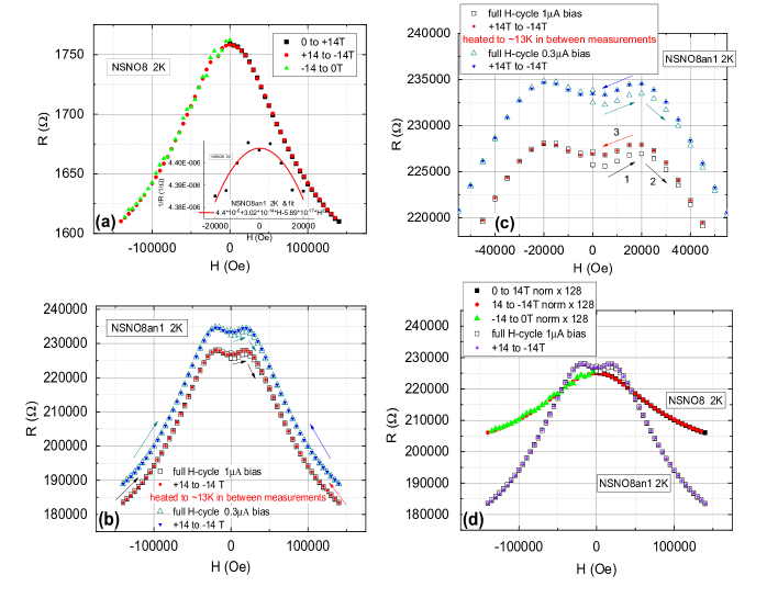
To further shed light on the insensitivity of the conductance spectra to magnetic fields in the present study, we measured the magnetoresistance of the as deposited and annealed NSNO8 films at 2 K. The results are shown in Fig. 7. Both films exhibit negative MR of 9% (NSNO8) and 20% (NSNO8an1) at 14 T, except for a slight positive MR between 2 T in the annealed film. Fig. 7 (d) shows comparison of the two films with normalization at zero field. In a recent study by Stupakov et al. of very similar well oxygenated films of Stupakov , negative MR similar to what we found in the as deposited film NSNO8, was observed and thoroughly investigated. They showed that the magnetic field Zeeman splitting of the localized states in the films is responsible for the negative MR. Our NSNO8 film is more disordered due to the Sr doping and the lower oxygen pressure used during its deposition process (100 vs 150 mTorr). Moreover, the films in Ref. Stupakov were further oxygenated at high temperature in 15 Torr Oxygen on the cool down step from 700 0C after deposition, while our annealing to extract Oxygen was carried out at a much lower temperature of 200 0C. Therefore, it is very likely that oxygen was mainly extracted from the grain boundaries of our films leaving the grains themselves unchanged. Nevertheless, the differences from Ref. Stupakov didn’t affect the MR significantly as our 7% MR in NSNO8 at 10 T is similar to their 7-9% MR at 10 T. The oxygen deficient NSNO8an1 is certainly much more disordered, much more resistive and its MR is about twice that (in %) of the NSNO8 film at 14 T as seen in Fig. 7 (d). It therefore follows that while the grains are presumably contributing to the negative MR in quite the same amount in both films, the more insulating grain boundaries in the NSNO8an1 film must contribute the second half of its MR.
A priori, the mechanism of the negative MR in the grain boundaries of our NSNO8an1 film is not necessarily the same as in Ref. Stupakov . A hint of the existence of a different mechanism is found in the low field positive MR data of Fig. 7 (b) and (c), which was absent in Stupakov . The initial small asymmetric hysteresis in this regime is pointing to some ordering in the high magnetic field which then keeps the MR curve symmetric with field cycling between 14 T without any hysteresis. However, after temperature cycling to about 13 K and back to 2 K, the initial asymmetric hysteresis returned. But after exposure to high field again, the MR remained symmetric under field cycling. Apparently, the increased temperature took the film above a magnetic induced ordering transition, and turned it back to its original state. It seems that this ordering of the film is robust (”hard”) at 2 K and if it were a ferromagnetic order, the sample is still below the coercive field even at 14 T. Another phenomenon seen in Fig. 7 (c) is the nearly parabolic dependence of the MR between 2 T. In the inset of Fig. 7 (a) this MR data is plotted as conductance 1/R vs H, and the resulting behavior is parabolic with a dominant term . This is typical of flux flow conductance in a superconductor Tinkham ; Koren . We note that Stupakov et al Stupakov didn’t observe the low field anomaly that we see between 2 T as in Fig. 7 (c), and we therefore can’t compare our results to their results in this regime. The low field MR seen in Fig. 7 (c) can not be attributed to weak antilocalization (WAL) either, since WAL functional behavior vs field near zero field is more like a square root of H HLN , rather than nearly parabolic in H as we observe.
Next we discuss whether the present MR results have any bearing on the field independent conductance as seen in Figs. 5 (a) and 6 (c). First, since the magnetic field induced ordering of the film as seen in the MR data is robust, it seems likely that unconventional same-spin triplet superconductivity is involved. Spin-singlet superconductivity should have been suppressed by the fields we applied of up to 4 T in the conductance measurements. Second, if superconductivity were present in our films, flux flow would yield negative parabolic-in-field conductance, and we do observe such a behavior between 2 T as seen in the inset to Fig. 7 (a). Third, the ordering in the MR measurements deduced from the hysteresis in Fig. 7 (c), resets itself after temperature cycling to 13 K and back to 2 K. This could be associated with a superconductive order that vanishes above the transition temperature which is less than 13 K. From the above discussion we conclude that superconductivity could be associated with the observed field-induced ordering in the MR results. Moreover, from the huge effect of the low temperature annealing (at 2000C) on the resistance of the films below 4 K as seen before, this superconductivity must reside in the grain boundary regions at the surfaces of the grains. Therefore, it looks as if the Josephson-like tunneling we observed in Fig. 6 is an interface effect of superconductivity with a low volume fraction. Possibly, the infinite layer phase of develops on the surface of the grains in our Oxygen deficient films and this is the source of the superconductivity signature that we observed. Local probe measurements such as scanning tunneling spectroscopy (STS) could detect the superconductive energy gap or gaps of this superconductor, being either or of a new one. The high film resistance though can make such STS measurements difficult.
IV Conclusions
We have demonstrated that our Oxygen deficient films exhibit Josephson-like tunneling characteristic with serial resistance. Though insulating due to the oxygen poor grain boundaries, the films show signatures of superconductivity in their energy gap opening, in their filling up of this gap with increasing temperature, and in their negative parabolic magnetoconductance typical of flux flow in superconductors. The insensitivity of the conductance spectra to magnetic fields, could be attributed to unconventional same-spin triplet superconductivity. The films can therefore be seen as comprised of a network of SIS tunneling junctions residing in the grain boundary regions, on the surface of the grains and the interface regions between them.
Acknowledgments:
We are grateful to Larisa Patlagan for her help and advice in preparing the ceramic target.
References
- (1) Danfeng Li, Kyuho Lee, Bai Yang Wang, Motoki Osada, Samue Crossley, Hye Ryoung Lee1, Yi Cui, Yasuyuki Hikita1 & Harold Y. Hwang, Superconductivity in an infinite-layer nickelate. Nature 572, 624 (2019).
- (2) Michael R. Norman, Entering the Nickel Age of Superconductivity. Physics 13, 85 (2020).
- (3) Danfeng Li, Bai Yang Wang, Kyuho Lee, Shannon P. Harvey, Motoki Osada, Berit H. Goodge, Lena F. Kourkoutis, and Harold Y. Hwang, Superconducting Dome in Infinite Layer Films. Phys. Rev. Lett. 125, 027001 (2020).
- (4) Motoki Osada, Bai Yang Wang, Berit H. Goodge, Kyuho Lee, Hyeok Yoon, Keita Sakuma, Danfeng Li, Masashi Miura, Lena F. Kourkoutis, Harold Y. Hwang, A superconducting praseodymium nickelate with infinite layer structure. Nano Lett. 20, 5735 (2020).
- (5) Qing Li, Chengping He, Jin Si, Xiyu Zhu, Yue Zhang, Hai-Hu Wen, Absence of superconductivity in bulk . Communications Materials volume 1, Article number: 16 (2020). arXiv:1911.02420 [cond-mat.supr-con].
- (6) Xiao-Rong Zhou, Ze-Xin Feng, Pei-Xin Qin, Han Yan, Shuai Hu, Hui-Xin Guo, Xiao-Ning Wang, Hao-Jiang Wu, Xin Zhang, Hong-Yu Chen, Xue-Peng Qiu, Zhi-Qi Liu, Absence of superconductivity in thin films without chemical reduction. Rare Met. 39, 368 (2020).
- (7) Shengwei Zeng, Chi Sin Tang, Xinmao Yin, Changjian Li, Zhen Huang, Junxiong Hu, Wei Liu, Ganesh Ji Omar, Hariom Jani, Zhi Shiuh Lim, Kun Han, Dongyang Wan, Ping Yang, Andrew T. S. Wee, Ariando Ariando, Phase diagram and superconducting dome of infinite-layer thin films. arXiv:2004.11281 [cond-mat.supr-con] April (2020).
- (8) Qiangqiang Gu, Yueying Li, Siyuan Wan, Huazhou Li, Wei Guo, Huan Yang, Qing Li, Xiyu Zhu, Xiaoqing Pan, Yuefeng Nie, Hai-Hu Wen, Two superconducting components with different symmetries in films. arXiv:2006.13123 [cond-mat.supr-con] June (2020).
- (9) Ying Xiang, Qing Li, Yueying Li, Huan Yang, Yuefeng Nie, Hai-Hu Wen, Magnetic transport properties of superconducting thin films. arXiv:2007.04884 [cond-mat.supr-con] July (2020).
- (10) G. Madhu, K. Maniammal and V. Biju, Defect induced ferromagnetic interaction in nanostructured nickel oxide with core–shell magnetic structure: the role of and vacancies. Phys. Chem. Chem. Phys. 18, 12135 (2016).
- (11) Dan Liu, Dongsheng Li and Deren Yang, Size-dependent magnetic properties of branchlike nickel oxide nanocrystals. AIP Advances 7, 015028 (2017).
- (12) X. Luo, L. T. Tseng, S. Li, J. B. Yi, Room temperature ferromagnetic ordering of NiO films through exchange coupling. Materials Science in Semiconductor Processing 30, 228 (2015).
- (13) Sayan Dey, Swarupananda Bhattacharjee, Mahua Ghosh Chaudhuri, Raj Shekhar Bose, Suman Halder and Chandan Kr. Ghosh, Synthesis of pure nickel(III) oxide nanoparticles at room temperature for Cr(VI) ion removal. RSC Adv. 5, 54717 (2015).
- (14) I. Shklovskii and A. L. Efros, Electronic Properties of Doped Semiconductors (Springer, Berlin, 1984) chap. 9.
- (15) B. Fisher, G. Koren, J. Genossar, L. Patlagan and E.L. Gartstein, Variable range hopping in . Physica C 176, 75 (1991).
- (16) Chengping He, Xue Ming, Qing Li, Xiyu Zhu, Jin Si, and Hai-Hu Wen, Synthesis and physical properties of perovskite (x = 0, 0.2) and infinite-layer nickelates. arXiv:2010.11777 [cond-mat.supr-con].
- (17) R. S. Keizer, S. T. B. Goennenwein, T. M. Klapwijk, G. Miao, G. Xiao and A. Gupta, A spin triplet supercurrent through the half-metallic ferromagnet . Nature 439, 825 (2006).
- (18) Y. Kalcheim, I. Felner, O. Millo, T. Kirzhner, G. Koren, A. Di Bernardo, M. Egilmez, M. G. Blamire, and J. W. A. Robinson, Magnetic field dependence of the proximity-induced triplet superconductivity at ferromagnet/superconductor interfaces. Phys. Rev. B 89, 180506(R) (2014).
- (19) A. F. Andreev, Zh. Eksp. Teor. Fiz. 46, 1823 (1964). [Sov. Phys. JETP 19, 1228 (1964).]
- (20) Oded Millo and Gad Koren, What can Andreev bound states tell us about superconductors? Phil. Trans. R. Soc. A 376 20140143 (2018).
- (21) R. Kleiner, F. Steinmeyer, G. Kunkel, and P. Muller, Intrinsic Josephson Effects in Single Crystals. Phys. Rev. Lett. 68, 2395 (1992).
- (22) V. M. Krasnov, A. Yurgens, D. Winkler, P. Delsing, and T. Claeson, Evidence for Coexistence of the Superconducting Gap and the Pseudogap in Bi-2212 from Intrinsic Tunneling Spectroscopy. Phys. Rev. Lett. 84, 5860 (2000).
- (23) Minoru Suzuki, Takashi Hamatani, Yoshiharu Yamada, Kenkichi Anagawa, and Takao Watanabe, Characteristic Relationship Between the Maximum Josephson Current and the c-Axis Conductivity Observed for Intrinsic Josephson Junctions in Bi-Sr-Ca-Cu-O. IEEE Trans. Appl. Supercon. 15, 189 (2005).
- (24) Goutam Sheet, S. Mukhopadhyay, and P. Raychaudhuri, Role of critical current on the point-contact Andreev reflection spectra between a normal metal and a superconductor. Phys. Rev. B 69, 134507 (2004)
- (25) H. Courtois, M. Meschke, J. T. Peltonen, and J. P. Pekola, Origin of Hysteresis in a Proximity Josephson Junction. Phys. Rev. Lett. 101, 067002 (2008).
- (26) G. Koren, Tunneling and bound states in near-edge junctions fabricated by deposition through a wire shadow mask. arXiv:1803.10046 [cond-mat.supr-con].
- (27) A. Stupakov, O. Pacherova, T. Kocourek, M. Jelinek, A. Dejneka, and M. Tyunina, Negative Magnetoresistance in epitaxial films of neodymium nickelate. Phys. Rev. B 99, 085111 (2019).
- (28) M. Tinkham, Resistive Transition of High-Temperature Superconductors. Phys. Rev. Lett. 61, 1658 (1998).
- (29) Gad Koren and Patrick A. Lee, Observation of two distinct pairs fluctuation lifetimes and supercurrents in the pseudogapregime of cuprate junctions. Phys. Rev. B 94, 174515 (2016).
- (30) Shinobu Hikami, Anatoly I. Larkin and Yosuke Nagaoka, Spin-Orbit Interaction and Magnetoresistance in the Two Dimensional Random System. Prog. Theor. Phys. 63, 707 (1980).