5pt
0.84(0.08,0.95) ©2019 IEEE. Personal use of this material is permitted. Permission from IEEE must be obtained for all other uses, in any current or future media, including reprinting/republishing this material for advertising or promotional purposes, creating new collective works, for resale or redistribution to servers or lists, or reuse of any copyrighted component of this work in other works. DOI: 10.1109/IEDM19573.2019.8993477
Ab initio mobility of mono-layer MoS2 and WS2: comparison to experiments and impact on the device characteristics
Abstract
We combine the linearized Boltzmann Transport Equation (LBTE) and quantum transport by means of the Non-equilibrium Green’s Functions (NEGF) to simulate single-layer MoS2 and WS2 ultra-scaled transistors with carrier mobilities extracted from experiments. Electron-phonon, charged impurity, and surface optical phonon scattering are taken into account with all necessary parameters derived from ab initio calculations or measurements, except for the impurity concentration. The LBTE method is used to scale the scattering self-energies of NEGF, which only include local interactions. This ensures an accurate reproduction of the measured mobilities by NEGF. We then perform device simulations and demonstrate that the considered transistors operate far from their performance limit (from 50% for MoS2 to 60% for WS2). Higher quality materials and substrate engineering will be needed to improve the situation.
I Introduction
Motivated by the first demonstration of a mono-layer MoS2 transistor [1] significant efforts have been undertaken to simulate the properties of devices based on 2-D transition metal dichalcogenides (TMDs). Their carrier mobility has been extensively modeled, starting with Ref. [2]: the phonon-limited mobility of MoS2 was computed with the linearized Boltzmann Transport Equation (LBTE) after extracting the required effective masses and electron-phonon coupling parameters from density-functional theory (DFT). Going one step further, the influence of charged impurity scattering was highlighted in Ref. [3], that of surface optical phonons in Ref. [4], in both cases in the effective mass approximation.
Accurately predicting the “current vs. voltage” characteristics of monolayer TMD transistors represents another challenge. It can be addressed with an ab initio quantum transport (QT) approach, e.g. the Non-equilibrium Green’s Functions (NEGF), expressed in a maximally localized Wannier function (MLWF) basis. As such calculations are computationally very demanding, they were first restricted to ballistic transport [5]. Electron-phonon scattering was later added, but in the form of parameterized self-energies [6]. Attempts were also made to treat the electrons, phonons, and their interactions at the ab initio level [7]. However, because of the diagonal approximation typically applied to the scattering self-energies, the obtained results may suffer from inaccuracies.
Here, we combine LBTE and NEGF, both from first-principles, to provide the first QT simulations of MoS2 and WS2 single-layer transistors with the same mobility values as in experiments. By considering electron-phonon (E-Ph), charged impurity (CI), and surface optical phonon (SOP) scattering, LBTE can reproduce the experimental mobility of these 2-D materials over a large temperature range. These results were then used to scale each diagonal scattering self-energy in NEGF so that our QT calculations produce the same mobilities as LBTE. The simulated “I-V” characteristics finally suggest that CI and SOP, whose magnitude can be altered by improving the 2-D crystal quality or by changing the substrate material, are responsible for a current reduction by a factor comprised between 1.7 (WS2) and 2 (MoS2), as compared to the case with E-Ph only (performance limit).
II Approach
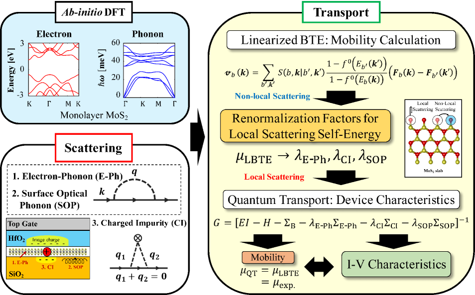
Our ab initio LBTE+QT approach is summarized in Fig. 1. As first step, the electronic structures of the primitive unit cell corresponding to a 2-D monolayer were computed with VASP [8] within the generalized gradient approximation (GGA) of Perdew, Burke, and Ernzerhof (PBE) [9]. For transport calculations, the resulting plane-wave DFT results were projected onto a MLWF basis [10] to produce a tight-binding-like Hamiltonian [11]. The dynamical matrices required for the phonon frequencies were generated via density-functional perturbation theory (DFPT) and the Phonopy code [12].
For each interaction type (E-Ph, CI, and SOP), a specific scattering self-energy (NEGF) and transition probability function (LBTE) was constructed from the prepared DFT data and the corresponding Feynman diagram. In case of E-Ph, the equations of Refs. [11] and [13] were implemented for NEGF and LBTE, respectively. The electron-SOP coupling was modeled by taking into account the vibrations of the dielectric environments surrounding the 2-D monolayers [4]. The phonon frequencies and coupling strengths were taken from measurements [14]. Finally, the electron-CI interactions were cast into a Coulomb potential with image charges [3] using the impurity concentration as fitting parameter. 2-D screening caused by the surrounding dielectrics was applied to damp SOP and CI scattering.
For each 2-D material, three mobilities , , and were calculated with the modified LBTE solver of Ref. [13], accounting for local and non-local energy-momentum transitions. Available temperature-dependent experimental data were then reproduced by adjusting only. Next, the same mobilities were computed with NEGF using the “dR/dL” method [15] and assuming diagonal scattering self-energies. By comparing the values obtained with LBTE and NEGF, renormalization factors (, , and ) could be determined to scale , , and , ensuring that NEGF returns the same mobility as LBTE and experiments. Taking advantage of the “calibrated” NEGF simulator [11], the I-V characteristics of 2-D devices could be accurately predicted.
III Results
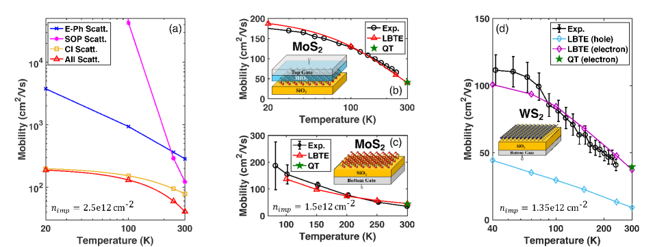
The low-field mobility of MoS2 and WS2 monolayers as a function of temperature is reported in Fig. 2. Three cases were investigated: MoS2 deposited on a 270 nm-thick bottom SiO2 substrate (i) with and (ii) without a 30 nm-thick top HfO2 layer and (iii) WS2 with the same substrate as (ii). For the MoS2 configuration (i), the temperature-dependence of the E-Ph-, SOP-, and CI-limited mobilities, as obtained with LBTE, is plotted in Fig. 2(a), together with the total mobility calculated by Matthiessen’s rule. The impurity concentration was set to =2.5e12 cm-2, which leads to an excellent agreement with the experimental data of Ref. [16] (Fig. 2(b)). It can be seen that CI scattering is the limiting factor at all temperatures, but SOP kicks in at high temperatures and induces a significant mobility drop. The LBTE mobilities of the second MoS2 sample (Fig. 2(c), =1.5e12 cm-2) [17] and of WS2 (Fig. 2(d), =1.35e12 cm-2) [18] reveal an equally good agreement with experiments. In Fig. 2 we also provide the room-temperature QT mobilities with renormalized scattering self-energies to validate our scheme.
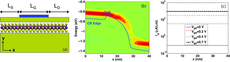
As next step, the “current vs. voltage” characteristics of MoS2 and WS2 monolayer field-effect transistors (FETs) are analyzed. The selected benchmark structure is shown in Fig. 3(a): a single-gate (SG) FET with a gate length =15 or 50 nm, source/drain-extensions of ==15 nm each, and a supply voltage =0.7 V. The 2-D materials were deposited on a SiO2 “substrate” with a top HfO2 layer of thickness =3 nm and a relative permittivity =20. Ohmic contacts were assumed with a donor concentration =5e13 cm-2. Hence, the effect of contact resistances was neglected. To verify that the QT scattering models properly work, the energy- and position-resolved current of the WS2 FET is depicted in Fig. 3(b), including E-Ph, SOP, and CI interactions, while current conservation is demonstrated in Fig. 3(c) for different gate biases. As expected, electrons lose a substantial amount of their energy on the drain side of the transistor, where the electric field reaches its maximum.
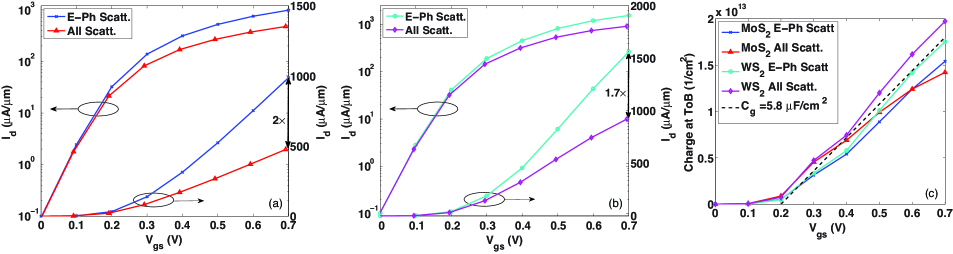
The - transfer characteristics of both FET types are shown in Figs. 4(a-b). Two curves per device were computed. First, as a reference, the current with electron-phonon scattering only is given. This mechanism cannot be eliminated, contrary to CI that can be reduced by improving the crystal quality or SOP that could possibly be minimized by carefully choosing the substrate material. The second curve includes all scattering sources and uses the impurity concentrations and scaling factors from Fig. 2. A strong ON-current decrease caused by SOP and CI is found. It is larger in MoS2 than in WS2 (2 vs. 1.7) due to the presence of more charged impurities (=2.5 vs. 1.35 cm-2). Consequently, both FETs operate far from their optimum, defined as the current with E-Ph scattering only. It can be noticed in Fig. 4(c) that the gate capacitance =5.8 F/cm2 extracted from the derivative of the electron concentration at the top-of-the-barrier with respect to the gate voltage does not suffer from so-called density-of-states bottlenecks as it approaches the value of =/=5.9 F/cm2, the oxide capacitance.
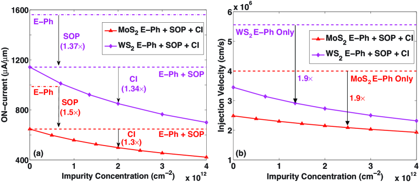
The influence of SOP and CI is examined in Fig. 5(a) where the ON-current values of the MoS2 and WS2 FETs are plotted as a function of the impurity concentration . The cases with E-Ph scattering only, E-Ph+SOP, and E-Ph+SOP+CI are supplied, thus isolating the impact of each scattering mechanism from the others. It appears that SOP contributes slightly more to the current decrease than CI (factor 1.37-1.5 vs. 1.3-1.34), for both 2-D materials, contrary to what was observed in mobility calculations (CI-limited). This seems to indicate that the emission/absorption of SOP is enhanced under high-field conditions. The corresponding injection velocities at the top-of-the-barrier follow in Fig. 5(b). Thanks to their lower effective mass (=0.30 vs. 0.46 ), electrons in WS2 are faster than in MoS2, but their velocity could still be improved by a factor 2, as compared to the present case, if both SOP and CI were removed. The extracted velocities however degrade when the gate length increases to 50 nm, as can be seen in Table 5(c). The latter summarizes the key mobility, ON-current, and injection velocity results obtained here.
IV Conclusion
We proposed an ab initio LBTE+QT framework to compute the transport properties of 2-D materials. It relies on the renormalization of the NEGF self-energies with scaling factors determined from LBTE. The mobility of MoS2 and WS2 monolayers was accurately modeled with this method, which also helped predict the “I-V” characteristics of monolayer MoS2 and WS2 FETs with short gate lengths. Further device progresses will depend on improved materials and careful design choices. The developed environment is now ready to explore novel 2-D compounds beyond TMDs.
Acknowledgment
This work was supported the MARVEL National Centre of Competence in Research of the Swiss National Science Foundation (SNSF), by SNSF under Grant No. 175479 (ABIME), and by a grant from the Swiss National Supercomputing Centre (CSCS) under Project s876.
References
- [1] B. Radisavljevic et al., Nat. Nano. 6, 147 (2011).
- [2] K. Kaasbjerg et al., Phys. Rev. B 85, 115317 (2012).
- [3] Z.-Y. Ong et al., Phys. Rev. B 88, 165316 (2013).
- [4] N. Ma and D. Jena, Phys. Rev. X 4, 011043 (2014).
- [5] J. Chang et al., App. Phys. Lett. 103, 223509 (2013).
- [6] A. Sengupta et al., AIP Advances 5, 027101 (2015).
- [7] M. Luisier et al., Proc. of IEDM 2016, 5.4.1-5.4.4 (2016).
- [8] G. Kresse and J. Furthmüller, Phys. Rev. B 54, 11169 (1996).
- [9] J. P. Perdew et al., Phys. Rev. Lett. 77, 3865 (1997).
- [10] A. A. Mostofi et al., Comp. Phys. Comm. 178, 685-699 (2008).
- [11] A. Szabó et al., Phys. Rev. B 92, 035435 (2015).
- [12] A. Togo et al., Phys. Rev. B 78, 134106 (2008).
- [13] R. Rhyner and M. Luisier, J. Appl. Phys. 114, 223708 (2013).
- [14] K. Zou et al., Phys. Rev. Lett. 105, 126601 (2010).
- [15] K. Rim et al., Proc. of IEDM 2002, 43-46 (2002).
- [16] B. Radisavljevic and A. Kis, Nat. Mat. 12, 815 (2013).
- [17] K. K. H. Smithe et al., Nano. Lett. 18, 4516 (2018).
- [18] D. Ovchinnikov et al., ACS Nano 8, 8174-8181 (2014).
| (c) | MoS2 | WS2 | |
| Mobility (cm2/Vs) | E-Ph | 283.9 | 357.7 |
| CI | 79.1 | 44.0 | |
| SOP | 122.1 | 793.4 | |
| Total | 41.1 | 37.4 | |
| 15 nm | (mA/m) | 0.476 | 0.921 |
| (cm/s) | 2.1e6 | 2.9e6 | |
| 50 nm | (mA/m) | 0.264 | 0.513 |
| (cm/s) | 8.3e5 | 1.3e6 |