Highly anisotropic two-dimensional metal in monolayer MoOCl2
Abstract
Anisotropy is a general feature in materials. Strong anisotropy could lead to interesting physical properties and useful applications. Here, based on first-principles calculations and theoretical analysis, we predict a stable two-dimensional (2D) material—the monolayer MoOCl2, and show that it possesses intriguing properties related to its high anisotropy. Monolayer MoOCl2 can be readily exfoliated from the van der Waals layered bulk, which has already been synthesized. We show that a high in-plane anisotropy manifests in the structural, phononic, mechanical, electronic, and optical properties of monolayer MoOCl2. The material is a metal with highly anisotropic Fermi surfaces, giving rise to open orbits at the Fermi level, which can be probed in magneto-transport. Remarkably, the combination of high anisotropy and metallic character makes monolayer MoOCl2 an almost ideal hyperbolic material. It has two very wide hyperbolic frequency windows from 0.41 eV (99 THz) to 2.90 eV (701 THz), and from 3.63 eV (878 THz) to 5.54 eV (1340 THz). The former window has a large overlap with the visible spectrum, and the dissipation for most part of this window is very small. The window can be further tuned by the applied strain, such that at a chosen frequency, a transition between elliptic and hyperbolic character can be induced by strain. Our work discovers a highly anisotropic 2D metal with extraordinary properties, which holds great potential for electronic and optical applications.
I Introduction
Two-dimensional (2D) materials have been attracting tremendous interest because of their fascinating properties, excellent tunability, and promising applications Das et al. (2015); Novoselov et al. (2005); Bhimanapati et al. (2015a); Tan et al. (2017); Bhimanapati et al. (2015b). Similar to 3D crystals, most 2D materials are stabilized in high-symmetry structures, which are usually preferred for minimizing the energy. For example, graphene Novoselov et al. (2004), hexagonal BN Nagashima et al. (1995), H- and T-phase transition metal dichalcogenides Mak et al. (2010); Eda et al. (2011), and most MXenes Naguib et al. (2011) have threefold rotational symmetry. It follows that their properties should be isotropic in the 2D plane.
There do exist 2D anisotropic materials, such as the black phosphorene Li et al. (2014); Ling et al. (2015); Çak ır et al. (2015), the similarly structured group-V monolayers Lu et al. (2016); Zeraati et al. (2016); Rehman et al. (2020), and 2D group-IV monochalcogenides Chang et al. (2016). It was realized that the anisotropy could be an advantage of these materials for controlling the directional transport of charge carriers or plasmonic waves Fei and Yang (2014); Guan et al. (2018); Nemilentsau et al. (2016), for generating ferroelectricity Fei et al. (2016); Xiao et al. (2018), for tuning light absorption with selective polarization Qiao et al. (2014), and etc.
Particularly, it was proposed that highly anisotropic metals could be good candidates for hyperbolic materials Sun et al. (2014); Guan et al. (2017), which means the real parts of their permittivity tensor elements take different signs Poddubny et al. (2013); Smith and Schurig (2003); Alekseyev et al. (2012a). Such materials have a special hyperbolic-type light dispersion, which can produce extraordinary optical properties, like all-angle negative refraction Smith et al. (2004); Hoffman et al. (2007); Yao et al. (2008), sub-wavelength imaging Liu et al. (2007a); Lu and Sridhar (2008); Rho et al. (2010), and strongly enhanced spontaneous emission Jacob et al. (2012); Yang et al. (2012); Cortes et al. (2012). The idea was explored in several 3D layered materials Sun et al. (2014, 2011); Alekseyev et al. (2012b); Esslinger et al. (2014); Korzeb et al. (2015), and the class of electride compounds such as Ca2N was predicted to be ideal candidates because of their wide hyperbolic frequency window and suppressed dissipation Guan et al. (2017). For 2D, the aforementioned anisotropic materials such as black phosphorene could work, but they require additional charge doping Nemilentsau et al. (2016). Besides, the anisotropic is not so strong, which limits the hyperbolic frequency window, and the sizable dissipation due to light absorption is also an issue. The situation therefore calls for an exploration of new 2D materials, which are intrinsically metallic and possess a high anisotropy.
MoOCl2 is a typical van der Waals (vdW) layered material. In a recent experiment Wang et al. (2020), it was found that the material is a good metal with strong anisotropy in the layer plane, and thin flakes can be easily exfoliated from the bulk sample. Motivated by this finding, in this work, we perform a systematic study of MoOCl2 in the 2D limit, based on the first-principles calculations. We show that monolayer MoOCl2 is stable and has low binding energy to the bulk. The lattice structure has a strong in-plane anisotropy, with binding much stronger in one direction than the other. We demonstrate that this strong anisotropy manifests in various physical properties, including the sound speed, the Young’s modulus, the electronic band dispersion, the Fermi surface geometry, the optical properties, and the strain response. Remarkably, we find that monolayer MoOCl2 is an almost ideal 2D hyperbolic material. It has two wide hyperbolic windows from 0.41 eV (99 THz) to 2.90 eV (701 THz) and from 3.63 eV (878 THz) to 5.54 eV (1340 THz). The former window overlaps with a large portion of the visible light. Moreover, for most part of this window, the absorption is very small. Our work reveals extraordinary properties of monolayer MoOCl2, which hold great potential for nanoscale electronic, mechanic, and optical applications.
II Calculation Method
Our first-principles calculations were based on the density functional theory (DFT), as implemented in the Vienna ab-initio Simulation Package (VASP) Kresse and Furthmüller (1996, 1996). The projector augmented wave (PAW) pseudo-potentials were adopted in the calculation Kresse and Joubert (1999); Blöchl (1994). The generalized gradient approximation with the Perdew-Burke-Ernzerhof (PBE) realization Perdew et al. (1996) was used for the exchange-correlation functional. The valence electrons treated in the calculations include Mo (), O (), and Cl (). The kinetic energy cutoff was fixed to 500 eV. For the self-consistent calculations, the Brillouin zone (BZ) integration was performed on a -centered mesh of -points. The energy and force convergence criteria were set to be 10-7 eV and 0.001 eV, respectively. A vacuum layer with 40 Å thickness was taken to avoid artificial interactions between periodic images, and this layer was subtracted when obtaining the proper permittivity of the monolayer Guan et al. (2015); Laturia et al. (2018). The optical properties were calculated by the FP-LAPW WIEN2k package Blaha et al. (2018). The plane wave cut-off parameter was set by . The k-point mesh for the self-consistent loop was the same as the VASP input, and it was increased to for the optical conductivity calculation. The phonon dispersion was calculated by using a 33 supercell. The force constants were calculated by VASP, and the pre-process and the post-process were performed by using the Phonopy code Togo and Tanaka (2015); Togo et al. (2010). Non-analytical term correction (NAC) was considered in treating the long range interaction of macroscopic electric field induced by the polarization of the collective ionic motions near the -point Gonze et al. (1994); Gonze and Lee (1997).
III Crystal structure, phonon, and mechanical properties
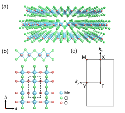
The experimental realization of bulk MoOCl2 was reported more than 50 years ago, by using the chemical vapor transport method Schäfer and Tillack (1964). Bulk MoOCl2 is a vdW layered material with NbOCl2-type crystal structure (space group ), as depicted in Fig. 1(a). Each layer in the structure consists of three atomic layers: the central layer contains Mo and O atoms, whereas the upper and the lower layers are of Cl atoms. The properties of bulk MoOCl2 have been studied in Ref. Wang et al. (2020). In this work, we shall focus on MoOCl2 in the monolayer form.
Because of the weak vdW bonding, we expect that a single layer of MoOCl2 can be readily exfoliated from the bulk sample. To have a quantitative assessment, we calculate the interlayer binding energy, defined as
| (1) |
where , , and are the energies of monolayer, layers, and layers, respectively, and is the in-plane area. Formally, should take the limiting value when approaches infinity. In practice, for vdW layered materials, typically has a quick saturation after first few layers. In our calculation, we take , where the convergence is achieved within 0.1 meV/Å2. The obtained binding energy for monolayer MoOCl2 is 18.0 meV/Å2. This value is comparable to graphene Liu et al. (2012); Wang et al. (2015) ( to meV/Å2) and monolayer MoS2 Bastos et al. (2019) ( meV/Å2), suggesting that monolayer MoOCl2 can also be obtained via mechanical exfoliation from the bulk sample.
The fully relaxed structure of monolayer MoOCl2 is illustrated in Fig. 1(b). The structure can be viewed as consisting of parallel Mo-O chains running along the ( vector) direction, and these chains are connected by the Cl atoms. It has a rectangular lattice with space group . The symmetry elements in the group include the twofold rotations along the three orthogonal direction, the inversion, and three mirror planes (). Clearly, the structure is anisotropic in the 2D plane. The optimized lattice constants are given by Å and Å. The detailed atomic positions are listed in Table 1.
| Site | Wyckoff symbol | |||
|---|---|---|---|---|
| Mo1 | 2 | 0.500 | 0.787 | 0.500 |
| O1 | 2 | 0.000 | 0.218 | 0.500 |
| Cl1 | 2 | 0.500 | 0.000 | 0.467 |
| Cl2 | 2 | 0.500 | 0.500 | 0.473 |
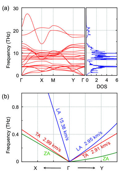
To investigate the stability of monolayer MoOCl2, we calculated its phonon spectrum. The obtained result is plotted in Fig. 2(a). One observes that there is no soft mode in the spectrum, indicating that the structure is dynamically stable. Around the point and at low frequencies, one finds the three acoustic phonon branches (see Fig. 2(b)). The lower branch is for the out-of-plane acoustic (ZA) phonon modes, which typically has a quadratic dispersion and is regarded as a characteristic for 2D materials Liu et al. (2007b); Zhu et al. (2014). The other two branches correspond to the longitudinal acoustic (LA) and transverse acoustic (TA) modes, which have linear dispersions. Their slopes give the sound velocities in the lattice. From the result in Fig. 2(b), we find that the LA and TA phonon velocities along the direction (along the vector) are 15.35 km/s and 2.99 km/s, whereas the corresponding values for the direction (along the vector) are 2.95 km/s and 2.91 km/s. One observes that the LA phonon velocity along is more than 5 times larger than that along . As the LA phonon velocity reflects the bonding strength in that direction, this large anisotropy indicates that the monolayer MoOCl2 structure is strongly coupled along , i.e., along the Mo-O chains (for reference, the LA phonon velocity in graphene is 19.9 km/s Cong et al. (2019)), whereas the coupling along , i.e., between the Mo-O chains, is much weaker.
| Elastic constants (N/m) | Young’s modulus (N/m) | Poisson’s ratio | ||||||
|---|---|---|---|---|---|---|---|---|
| ML-MoOCl2 | 279.3 | 80.0 | 2.7 | 18.5 | 279.3 | 80.0 | 0.034 | 0.010 |
| Graphene Andrew et al. (2012) | 352.7 | 352.7 | 60.9 | 145.9 | 342.2 | 342.2 | 0.173 | 0.173 |
We further investigate the mechanical properties of monolayer MoOCl2, including the elastic constants (), Young’s Modulus () and Poisson’s ratio (). Our results are listed in Table 2. One finds that the obtained elastic constants satisfy the mechanical stability criterion for rectangular lattices Mouhat and Coudert (2014):
| (2) |
which further demonstrates that the monolayer is stable. Again, strong anisotropy is observed in Young’s modulus and Poisson’s ratio for the two in-plane directions. Notably, Poisson’s ratio of monolayer MoOCl2 is much less than most 2D materials Andrew et al. (2012); Bosak et al. (2006); Zhang and Wang (2011), implying that the material could be useful for making flexible devices.
IV Electronic Structure
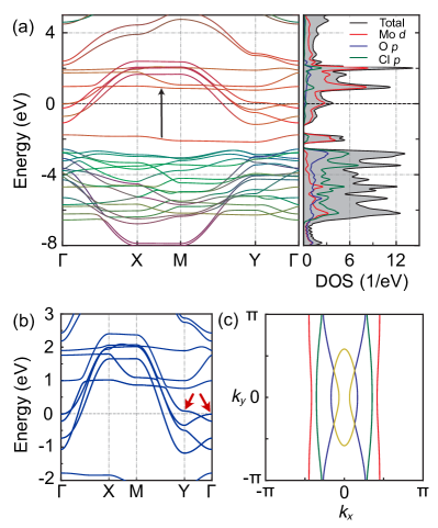
Next, we investigate the electronic band structure of monolayer MoOCl2. The result obtained from our DFT calculation is plotted in Fig. 3(a), along with orbital projected density of states (DOS). The effect of spin-orbit coupling (SOC) on the low-energy bands is found to be small, so the result shown here is without SOC (the result with SOC is presented in the Supplemental Material Sup ). From Fig. 3(a), one finds that monolayer MoOCl2 is a metal. The low-energy states around the Fermi level are mainly from the Mo- orbitals. The O- and Cl- orbitals are located away from the Fermi level (below eV).
Importantly, the band dispersion is highly anisotropic. There are four energy bands crossing the Fermi level. One can see that these bands are highly dispersive along the direction (e.g., - and - paths). In contrast, they become quite flat along the direction (e.g., - and - paths). This is consistent with our previous analysis that the monolayer is strongly coupled along the Mo-O chains, whereas the inter-chain coupling in the orthogonal direction is much weaker.
This strong anisotropy is also manifested in the Fermi surface geometry. Figure 3(c) shows the calculated Fermi surfaces (contours). These contours are strongly elongated along the direction, as a result of the weak band dispersion along . Notably, the strong anisotropy makes several contours cross the BZ boundary, giving rise to open orbits. The signature of such open orbits can be found in the magneto-transport, namely, the magneto-resistance can grow without limit when the applied magnetic field increases Ashcroft and Mermin (1976). This non-saturation behavior has been observed in bulk MoOCl2, which also has open orbits at the Fermi level along Wang et al. (2020).
Finally, we mention that there is a saddle point at very close to the Fermi level, as marked by the red arrow in Fig. 3(b). Around the point, the band energy increases (decreases) along the - (-) direction. According to the little group at , the band dispersion around this point should be described by
| (3) |
where eV is the energy of the saddle point. The two parameters and can be extracted from the DFT band dispersion. The results are eVÅ2 and eVÅ2. Their opposite signs conform with the saddle-like band dispersion. This type of band dispersion is another reflection of the strong in-plane anisotropy. Another saddle point can be observed at at energy 81 meV above the Fermi level. These saddle points contribute to the small peak in the DOS around the Fermi level.
V Hyperbolic optical property
As we mentioned at the very beginning, anisotropic metals naturally possess hyperbolic permittivity. To understand this point, we note that from the Drude model, for simple metals, the real parts of the permittivity tensor elements take the form of
| (4) |
where is the electron life-time broadening, and is the plasma frequency tensor element. The expression in Eq. (4) is an increasing function of . It takes negative value at low frequencies, and approaches when . Typically, for good metals, , so crosses zero when .
The plasma frequency tensor is an intrinsic band property, given by
| (5) |
where is the equilibrium distribution function, and () is the unit vector along the () direction. For our current 2D system with point group symmetry, only the diagonal elements and are non-vanishing. From (5), we see that each element is proportional to the squared band velocity along or averaged on the Fermi surface. Since we know from the band structure of monolayer MoOCl2 that the dispersion along is much weaker than along , we must have
| (6) |
It follows that and must cross zero at very different frequencies. Then, the frequency window between their zero points defines the hyperbolic window, in which and have opposite signs.
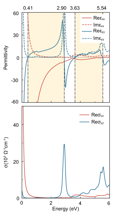
The above analysis is confirmed by our DFT calculation. In Fig. 4(a), we plot both real and imaginary parts of . In the calculation, we take meV, the value extracted from the transport measurement on the bulk sample at 10 K Wang et al. (2020). From the result, one clearly observes that there are two wide hyperbolic windows from 0.41 eV to 2.90 eV and from 3.63 eV to 5.54 eV, in which is positive whereas is negative. The former window is even wider than the previously reported one in Ca2N (from 0.38 eV to 1.40 eV) Guan et al. (2017), and it overlaps a large portion with the visible light spectrum. Moreover, one finds that the imaginary parts of the permittivity, which represent dissipation, are quite small for most part of this hyperbolic window (less than 1 from 1.58 eV to 2.30 eV). All these characters are much desired for applications. 2D materials with such ideal hyperbolic properties have not been reported before.
To take a closer look at optical absorption, in Fig. 4(b), we plot the real parts of the optical conductivities. They are connected with the imaginary parts of , because of the fundamental relation
| (7) |
One can see that because is much larger than , has a much stronger Drude peak (i.e., the peak close to zero frequency) than . However, is strongly suppressed above 0.70 eV in Fig. 4(b). In contrast, is suppressed between 0.09 eV and 2.54 eV, and it has a peak around 2.89 eV. By analyzing the band structure, we find this peak corresponds to the interband transitions between two almost parallel bands, as indicated by the arrow in Fig. 3(a). This dramatic difference between and indicates a strong linear optical dichroism, i.e., for incident lights with different linear polarizations, their absorption spectra will be very different.
VI Strain effect
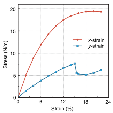
2D materials can usually sustain very large lattice strains (). And strain has been proved to be an effective method to tune the physical properties of 2D materials. Here we calculate the strain-stress relations for monolayer MoOCl2, and the result is plotted in Fig. 5. One observes that the curves for strains along and directions are quite different, again reflecting the large anisotropy. The critical strain for the direction is about 18%, and for the direction is about 15%. The large values of the critical strain demonstrate that monolayer MoOCl2 is quite flexible.
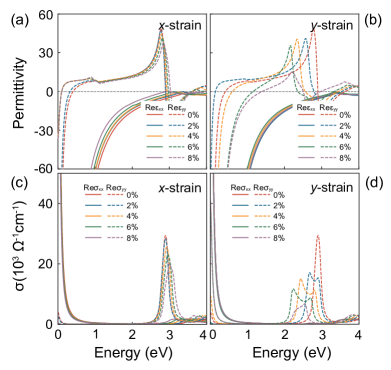
Then we consider the effect of strain on the physical properties of monolayer MoOCl2. We shall focus on the hyperbolic optical response below 4.0 eV, as it is the most interesting feature here. (The change in the band structure and the Fermi surface geometry is presented in the Supplemental Material Sup .) Figure 6(a-b) shows the calculated versus the applied uniaxial strains. Here, to simulate the stretching of a 2D sample, the strain is applied along or direction, and the structure is fully relaxed in the orthogonal direction. One observes that for tensile strains applied along (Fig. 6(a)), the hyperbolic window is gradually shifted to lower frequencies. Comparing the unstrained case and the 8% strained case, the hyperbolic window is red shifted from eV to eV. Meanwhile, for strains applied along (Fig. 6(b)), the change is more pronounced. While the change in is relatively small, the change in is quite large. The curve and its zero point first undergo a red shift at small strains, then they revert to a blue shift for strains greater than 4%. The hyperbolic window changes from eV at zero strain to eV at 8% strain. Thus, there is a range of frequencies, e.g., between 0.41 eV and 1.40 eV, in which the system is hyperbolic at zero strain but changed to elliptic at 8% strain. It follows that by tuning the applied strain, we can completely change the optical character of the material. This is a great advantage for applications.
In Fig. 6(c,d), we also plot the variation of versus the applied strain. The anisotropy (linear dichroism) remains large for these applied strains. Similar to the trend in Fig. 6(c), the change is more pronounced for strains applied along the direction. In Fig. 6(d), one observes that the single interband peak at 2.89 eV starts to split into two and red shift with increasing strain. These results will be useful for tuning the optical absorption of the material and for probing the strain via optical detection.
VII Discussion and Conclusion
We have revealed monolayer MoOCl2 as a highly anisotropic 2D metal. Such a character is quite unique among the existing 2D materials. Previously, the anisotropic feature has been mainly discussed in black phosphorene and related materials. However, these materials are intrinsically semiconductors, and their degree of anisotropy is not as high as monolayer MoOCl2. From our discussion, it is clear that the metallic character is important for its excellent hyperbolic optical property.
Besides the properties discussed here, the anisotropy will manifest in many other properties, such as the plasmonic waves, charge and thermal transport, and etc. And for 2D materials, there are many well developed approaches to tune their properties, such as the chemical modification, doping by adsorption, substitution, or gating. They may have pronounced effect on monolayer MoOCl2 and change its optical response. We hope our current work can motivate more subsequent studies on this interesting 2D material.
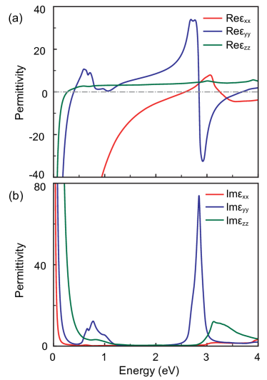
Finally, regarding the hyperbolic optical property, we note that bulk MoOCl2 is also an excellent candidate among 3D materials. The band structure of bulk MoOCl2 has been studied in Ref. Wang et al. (2020). Here, we calculate its permittivity and the result is shown in Fig. 7. One can see that there is also a large hyperbolic window between 0.39 eV and 2.57 eV, in which is negative, whereas the other two are positive. And Fig. 7(b) shows that the dissipation in the range 1.17 eV to 2.43 eV of this hyperbolic window is very small. Thus, bulk MoOCl2 could serve as a high-performance 3D hyperbolic material.
In conclusion, we have proposed a new 2D material—the monolayer MoOCl2. We predict that the monolayer could be easily obtained from the existing bulk sample by mechanical exfoliation. We have systematically investigated its physical properties, and revealed the material as a highly anisotropic 2D metal. The anisotropy originates from the underlying lattice structure, and manifests in a wide range of properties. The most prominent one uncovered here is the hyperbolic optical property. We show that the material hosts two wide hyperbolic windows from 0.41 eV and 2.90 eV and from 3.63 eV to 5.54 eV. The former window overlaps a large part of the visible spectrum and has very little dissipation. Such a characteristic is superior than all existing 2D materials, to our best knowledge. In addition, we demonstrate that the optical property can be effectively tuned by strain, and even a transition between hyperbolic and elliptic characters can be achieved. Our findings establish monolayer MoOCl2 as a unique addition to the 2D materials family. Its fascinating properties will complement other 2D materials and hold great promise for nanoscale electronic, mechanic, and optical applications.
Acknowledgements.
The authors thank Si Li, Shan Guan, Z. L. Liu, and D. L. Deng for valuable discussions. This work was supported by the National Natural Science Foundation of China (No. 11604273), and the Singapore Ministry of Education AcRF Tier 2 (MOE2019-T2-1-001).References
- Das et al. (2015) S. Das, J. A. Robinson, M. Dubey, H. Terrones, and M. Terrones, Annual Review of Materials Research 45, 1 (2015).
- Novoselov et al. (2005) K. S. Novoselov, D. Jiang, F. Schedin, T. J. Booth, V. V. Khotkevich, S. V. Morozov, and A. K. Geim, Proceedings of the National Academy of Sciences 102, 10451 (2005).
- Bhimanapati et al. (2015a) G. R. Bhimanapati, Z. Lin, V. Meunier, Y. Jung, J. Cha, S. Das, D. Xiao, Y. Son, M. S. Strano, V. R. Cooper, L. Liang, S. G. Louie, E. Ringe, W. Zhou, S. S. Kim, R. R. Naik, B. G. Sumpter, H. Terrones, F. Xia, Y. Wang, J. Zhu, D. Akinwande, N. Alem, J. A. Schuller, R. E. Schaak, M. Terrones, and J. A. Robinson, ACS Nano 9, 11509 (2015a).
- Tan et al. (2017) C. Tan, X. Cao, X.-J. Wu, Q. He, J. Yang, X. Zhang, J. Chen, W. Zhao, S. Han, G.-H. Nam, M. Sindoro, and H. Zhang, Chemical Reviews 117, 6225 (2017).
- Bhimanapati et al. (2015b) G. R. Bhimanapati, Z. Lin, V. Meunier, Y. Jung, J. Cha, S. Das, D. Xiao, Y. Son, M. S. Strano, V. R. Cooper, L. Liang, S. G. Louie, E. Ringe, W. Zhou, S. S. Kim, R. R. Naik, B. G. Sumpter, H. Terrones, F. Xia, Y. Wang, J. Zhu, D. Akinwande, N. Alem, J. A. Schuller, R. E. Schaak, M. Terrones, and J. A. Robinson, ACS Nano 9, 11509 (2015b).
- Novoselov et al. (2004) K. S. Novoselov, A. K. Geim, S. V. Morozov, D. Jiang, Y. Zhang, S. V. Dubonos, I. V. Grigorieva, and A. A. Firsov, Science 306, 666 (2004).
- Nagashima et al. (1995) A. Nagashima, N. Tejima, Y. Gamou, T. Kawai, and C. Oshima, Physical Review Letters 75, 3918 (1995).
- Mak et al. (2010) K. F. Mak, C. Lee, J. Hone, J. Shan, and T. F. Heinz, Phys. Rev. Lett. 105, 136805 (2010).
- Eda et al. (2011) G. Eda, H. Yamaguchi, D. Voiry, T. Fujita, M. Chen, and M. Chhowalla, Nano Letters 11, 5111 (2011).
- Naguib et al. (2011) M. Naguib, M. Kurtoglu, V. Presser, J. Lu, J. Niu, M. Heon, L. Hultman, Y. Gogotsi, and M. W. Barsoum, Advanced Materials 23, 4248 (2011).
- Li et al. (2014) L. Li, Y. Yu, G. J. Ye, Q. Ge, X. Ou, H. Wu, D. Feng, X. H. Chen, and Y. Zhang, Nature Nanotechnology 9, 372 (2014), 1401.4117 .
- Ling et al. (2015) X. Ling, H. Wang, S. Huang, F. Xia, and M. S. Dresselhaus, Proceedings of the National Academy of Sciences 112, 201416581 (2015), 1503.08367 .
- Çak ır et al. (2015) D. Çak ır, C. Sevik, and F. M. Peeters, Phys. Rev. B 92, 165406 (2015).
- Lu et al. (2016) Y. Lu, D. Zhou, G. Chang, S. Guan, W. Chen, Y. Jiang, J. Jiang, X.-s. Wang, S. A. Yang, Y. P. Feng, Y. Kawazoe, and H. Lin, npj Computational Materials 2, 16011 (2016), 1509.05629 .
- Zeraati et al. (2016) M. Zeraati, S. M. Vaez Allaei, I. Abdolhosseini Sarsari, M. Pourfath, and D. Donadio, Phys. Rev. B 93, 085424 (2016).
- Rehman et al. (2020) M. U. Rehman, C. Hua, and Y. Lu, Chinese Physics B 29, 057304 (2020).
- Chang et al. (2016) K. Chang, J. Liu, H. Lin, N. Wang, K. Zhao, A. Zhang, F. Jin, Y. Zhong, X. Hu, W. Duan, Q. Zhang, L. Fu, Q.-K. Xue, X. Chen, and S.-H. Ji, Science 353, 274 (2016).
- Fei and Yang (2014) R. Fei and L. Yang, Nano Letters 14, 2884 (2014), 1403.1003 .
- Guan et al. (2018) S. Guan, C. Liu, Y. Lu, Y. Yao, and S. A. Yang, Physical Review B 97, 144104 (2018).
- Nemilentsau et al. (2016) A. Nemilentsau, T. Low, and G. Hanson, Physical Review Letters 116, 066804 (2016), 1509.04383 .
- Fei et al. (2016) R. Fei, W. Kang, and L. Yang, Phys. Rev. Lett. 117, 097601 (2016).
- Xiao et al. (2018) C. Xiao, F. Wang, S. A. Yang, Y. Lu, Y. Feng, and S. Zhang, Advanced Functional Materials 28, 1707383 (2018).
- Qiao et al. (2014) J. Qiao, X. Kong, Z.-X. Hu, F. Yang, and W. Ji, Nature Communications 5, 4475 (2014).
- Sun et al. (2014) J. Sun, N. M. Litchinitser, and J. Zhou, ACS Photonics 1, 293 (2014).
- Guan et al. (2017) S. Guan, S. Y. Huang, Y. Yao, and S. A. Yang, Physical Review B 95, 165436 (2017).
- Poddubny et al. (2013) A. Poddubny, I. Iorsh, P. Belov, and Y. Kivshar, Nature Photonics 7 (2013), 10.1038/nphoton.2013.243.
- Smith and Schurig (2003) D. R. Smith and D. Schurig, Phys. Rev. Lett. 90, 077405 (2003).
- Alekseyev et al. (2012a) L. V. Alekseyev, V. A. Podolskiy, and E. E. Narimanov, Advances in OptoElectronics 2012, 1 (2012a).
- Smith et al. (2004) D. R. Smith, D. Schurig, J. J. Mock, P. Kolinko, and P. Rye, Applied Physics Letters 84, 2244 (2004).
- Hoffman et al. (2007) A. J. Hoffman, L. Alekseyev, S. S. Howard, K. J. Franz, D. Wasserman, V. A. Podolskiy, E. E. Narimanov, D. L. Sivco, and C. Gmachl, Nature Materials 6, 946 (2007).
- Yao et al. (2008) J. Yao, Z. Liu, Y. Liu, Y. Wang, C. Sun, G. Bartal, A. M. Stacy, and X. Zhang, Science 321, 930 (2008).
- Liu et al. (2007a) Z. Liu, H. Lee, Y. Xiong, C. Sun, and X. Zhang, Science 315, 1686 (2007a).
- Lu and Sridhar (2008) W. T. Lu and S. Sridhar, Physical Review B 77, 233101 (2008), 0710.4933 .
- Rho et al. (2010) J. Rho, Z. Ye, Y. Xiong, X. Yin, Z. Liu, H. Choi, G. Bartal, and X. Zhang, Nature Communications 1, 143 (2010).
- Jacob et al. (2012) Z. Jacob, I. I. Smolyaninov, and E. E. Narimanov, Applied Physics Letters 100, 181105 (2012), 0910.3981 .
- Yang et al. (2012) X. Yang, J. Yao, J. Rho, X. Yin, and X. Zhang, Nature Photonics 6, 450 (2012).
- Cortes et al. (2012) C. L. Cortes, W. Newman, S. Molesky, and Z. Jacob, Journal of Optics 14, 063001 (2012).
- Sun et al. (2011) J. Sun, J. Zhou, B. Li, and F. Kang, Applied Physics Letters 98, 101901 (2011).
- Alekseyev et al. (2012b) L. V. Alekseyev, V. A. Podolskiy, and E. E. Narimanov, Advances in OptoElectronics 2012, 1 (2012b).
- Esslinger et al. (2014) M. Esslinger, R. Vogelgesang, N. Talebi, W. Khunsin, P. Gehring, S. d. Zuani, B. Gompf, and K. Kern, ACS Photonics 1, 1285 (2014).
- Korzeb et al. (2015) K. Korzeb, M. Gajc, and D. A. Pawlak, Optics Express 23, 25406 (2015).
- Wang et al. (2020) Z. Wang, M. Huang, J. Zhao, C. Chen, H. Huang, X. Wang, P. Liu, J. Wang, J. Xiang, C. Feng, Z. Zhang, X. Cui, Y. Lu, S. A. Yang, and B. Xiang, Physical Review Materials 4, 041001 (2020).
- Kresse and Furthmüller (1996) G. Kresse and J. Furthmüller, Phys. Rev. B 54, 11169 (1996).
- Kresse and Furthmüller (1996) G. Kresse and J. Furthmüller, Comput. Mater. Sci. 6, 15 (1996).
- Kresse and Joubert (1999) G. Kresse and D. Joubert, Phys. Rev. B 59, 1758 (1999).
- Blöchl (1994) P. E. Blöchl, Phys. Rev. B 50, 17953 (1994).
- Perdew et al. (1996) J. P. Perdew, K. Burke, and M. Ernzerhof, Phys. Rev. Lett. 77, 3865 (1996).
- Guan et al. (2015) S. Guan, S. A. Yang, L. Zhu, J. Hu, and Y. Yao, Scientific Reports 5, 12285 (2015), 1502.02321 .
- Laturia et al. (2018) A. Laturia, M. L. V. d. Put, and W. G. Vandenberghe, npj 2D Materials and Applications 2, 6 (2018).
- Blaha et al. (2018) P. Blaha, K. Schwarz, G. K. H. Madsen, D. Kvasnicka, J. Luitz, R. Laskowski, F. Tran, and L. D. Marks, WIEN2k, An Augmented Plane Wave + Local Orbitals Program for Calculating Crystal Properties (Karlheinz Schwarz, Techn. Universität Wien, Austria, 2018).
- Togo and Tanaka (2015) A. Togo and I. Tanaka, Scr. Mater. 108, 1 (2015).
- Togo et al. (2010) A. Togo, L. Chaput, I. Tanaka, and G. Hug, Phys. Rev. B 81, 174301 (2010).
- Gonze et al. (1994) X. Gonze, J.-C. Charlier, D. Allan, and M. Teter, Physical Review B 50, 13035 (1994).
- Gonze and Lee (1997) X. Gonze and C. Lee, Physical Review B 55, 10355 (1997).
- Momma and Izumi (2011) K. Momma and F. Izumi, Journal of Applied Crystallography 44, 1272 (2011).
- Schäfer and Tillack (1964) H. Schäfer and J. Tillack, Journal of the Less Common Metals 6, 152 (1964).
- Liu et al. (2012) Z. Liu, J. Z. Liu, Y. Cheng, Z. Li, L. Wang, and Q. Zheng, Phys. Rev. B 85, 205418 (2012).
- Wang et al. (2015) W. Wang, S. Dai, X. Li, J. Yang, D. J. Srolovitz, and Q. Zheng, Nature Communications 6, 7853 (2015).
- Bastos et al. (2019) C. M. O. Bastos, R. Besse, J. L. F. Da Silva, and G. M. Sipahi, Phys. Rev. Materials 3, 044002 (2019).
- Liu et al. (2007b) F. Liu, P. Ming, and J. Li, Physical Review B 76, 064120 (2007b).
- Zhu et al. (2014) L. Zhu, G. Zhang, and B. Li, Physical Review B 90, 214302 (2014), 1409.1967 .
- Cong et al. (2019) X. Cong, Q.-Q. Li, X. Zhang, M.-L. Lin, J.-B. Wu, X.-L. Liu, P. Venezuela, and P.-H. Tan, Carbon 149, 19 (2019).
- Andrew et al. (2012) R. C. Andrew, R. E. Mapasha, A. M. Ukpong, and N. Chetty, Phys. Rev. B 85, 125428 (2012).
- Mouhat and Coudert (2014) F. Mouhat and F. m. c.-X. Coudert, Phys. Rev. B 90, 224104 (2014).
- Bosak et al. (2006) A. Bosak, J. Serrano, M. Krisch, K. Watanabe, T. Taniguchi, and H. Kanda, Phys. Rev. B 73, 041402 (2006).
- Zhang and Wang (2011) H. Zhang and R. Wang, Physica B: Condensed Matter 406, 4080 (2011).
- (67) See Supplemental Material at [url] for the band structure with SOC, and the effects of strain on band structures and FSs. .
- Ashcroft and Mermin (1976) N. Ashcroft and N. Mermin, Solid State Physics (Saunders College Publishing, 1976).