Electrical properties of SmB6 thin films
prepared by pulsed laser deposition
from a stoichiometric SmB6 target
Abstract
Possible existence of topologically protected surface in samarium hexaboride has created a strong need for investigations allowing to distinguish between properties coming from the surface states and those originating in the (remaining) bulk. Studies of SmB6 thin films represent a favorable approach allowing well defined variations of the bulk volume that is not affected by surface states. Moreover, thin films are highly desirable for potential technology applications. However, the growth of SmB6 thin films is accompanied by technology problems, which are typically associated with maintaining the correct stoichiometry of samarium and boron. Here we present feasibility study of SmB6 thin film synthesis by pulsed laser deposition (PLD) from a single stoichiometric SmB6 target. As proved by Rutherford Backscattering Spectrometry (RBS), we succeeded to obtain the same ratio of samarium and boron in the films as that in the target. Thin films revealing characteristic electrical properties of (crystalline) SmB6 were successfully deposited on MgO, sapphire, and glass-ceramics substrates, when the substrates were kept at temperature of 600 ∘C during the deposition. Performed electrical resistance studies have revealed that bulk properties of the films are only slightly affected by the substrate. Our results indicate that PLD is a suitable method for complex and intensive research of SmB6 and similar systems.
keywords:
rare earth alloys and compounds, thin films, vapor deposition, electrical transport, valence fluctuations, Rutherford backscattering, RBS1 Introduction
Heavy fermion semiconductor samarium hexaboride, SmB6, attracts attention of researchers for more than half a century. Its fascinating physical properties are very interesting not only because of long-lasting fundamental questions, but also from an application point of view [1, 2, 3, 4]. Electrical resistivity of high-quality SmB6 samples below 50 K shows a rapid increase with decreasing temperature, and surprisingly, it tends to saturate at very high residual value at the lowest temperatures, below 4 K [5, 6, 7]. Recently, SmB6 has been predicted to be a prototype of topological Kondo insulator [8, 9, 10, 11], and the strange low-temperature behavior is being explained by the metallic surface, whereas nontrivial topological surface states [8, 9, 10, 11], as well as ”trivial” polarity-driven ones [12] were proposed to exist there. Valence-fluctuation induced hopping transport [13] is another possibility to explain the puzzling electrical transport in SmB6 at the lowest temperatures [13]. In principle, all the mentioned scenarios could even coexist, nevertheless, the highest attention is paid to the SmB6 being a possible topological Kondo insulator.
Topological insulators represent an interesting new class of materials that is promising for both fundamental and applied research [3]. The surface states being robust against scattering from non-magnetic impurities and displaying spin-momentum locking predict a possible effective use of topological insulators in spintronics, magneto-electrics, and quantum computing [3, 4, 14, 15]. However, utilization of the surface transport is often complicated by residual conductivity of the bulk [3]. Advantage of SmB6 should be that it is expected to be a true topological insulator, i.e. with zero residual bulk conductivity, which is highly desired from application point of view [3]. As reported recently, the bulk electrical resistivity of SmB6 is thickness independent [16, 17], and the electrical conduction of SmB6 samples with different thickness can be adequately described by varying relative ratio of the bulk and surface contribution to the total conduction [17]. For further progress in both, understanding the underlying physics and development of possible applications, ongoing research is needed and reproducible fabrication of well defined SmB6 thin films allowing to control relative contributions from the bulk and the surface is highly desired. However, preparation of stoichiometric SmB6 thin films is not straightforward. Recently, semi-epitaxial SmB6 thin films were prepared by the molecular beam epitaxy with the obtained ratio of B to Sm between 4.9 and 5.7 [18]. Also two another groups reported a failure in attempts to deposit SmB6 thin films via pulsed laser deposition (PLD) using a single SmB6 target [16, 3]. As reported there, one of the main difficulties at depositing SmB6 is escape of boron [16], which leads to boron deficient films. To overcome this issue and achieve the correct stoichiometry, either co-sputtering of SmB6 and boron targets [3, 4] (using the combinatorial composition-spread approach [19]) or alternating ablation of SmB6 and boron targets [16] was finally used by those groups. On the other hand, it is worth to mention that almost 30 years ago SmB6 thin films were prepared by evaporating the bulk material onto glass-ceramic substrates, while those films revealed electrical properties as typical for semiconducting behavior of SmB6, as well as metalic-like conduction associated by the authors with the surface properties [20]. The mentioned work [20] indicates that it could be possible to obtain SmB6 thin films by deposition only from a single stoichiometric SmB6 target.
Our aim has been to prove possibility to prepare SmB6 thin films from a single SmB6 target by PLD technology, which is widespread in laboratory research due to easy adaptation of deposition equipment and variability of applied deposition parameters. Moreover, among methods for thin film deposition the PLD is considered to achieve very close correspondence between the target composition and the deposited film. In this work we report feasibility studies of SmB6 thin film synthesis by PLD from a single stoichiometric SmB6 target on several types of substrates and compare their properties with those of the target.
2 Experimental
SmB6 thin films were deposited by PLD from a commercially available polycrystalline SmB6 target (Testbourne, England). Nominal purity of the material was 99.5 , while the most contained contaminants reported were Si (0.02 ), Al (0.01 ), and Fe (0.01 ). The target was of disc geometry (25 mm in diameter, 5 mm thick). Nd: YAG laser was used to generate laser pulses of wavelength 355 nm and 532 nm at frequency of 2 Hz or 5 Hz. The 10 ns pulses with energy from the interval of 4 - 60 mJ were used to obtain the growth rate in the range of Å/s. The base pressure in the deposition chamber was 5 10-8 mbar. Several types of substrate material were used: glass, MgO single crystal, sapphire, and glass-ceramics (GC), namely, the non-polished ultra-low expansion GC CLEARCERAM®-Z (Ohara, Japan). Orientations of single crystal substrates were (001) and (012) for MgO and sapphire, respectively. The substrate temperature during the deposition was defined by the temperature of substrate holder that was kept at ambient temperature (glass, GC), or heated to 600 ∘C (MgO, sapphire, GC).
Elemental composition of the thin films deposited on glass substrates (at ambient temperature) was determined by Rutherford Backscattering Spectrometry (RBS) at Nuclear Physics Institute of the Czech Academy of Sciences on Tandetron 4130 MC accelerator. Ion beams of He+ and H+ ions with an energy of 2 MeV were used, while the ion beam incoming angles were 0∘ and 45∘. The glancing ion beam incoming angle was chosen in case of very thin layers characterization to increase the depth resolution. Detection of backscattered ions was performed by the ion implanted detector ULTRA ORTEC in IBM geometry with scattering angle of 170∘. The detector was placed at the angle of 10∘ with respect to the incident beam. The RBS spectra were evaluated using the SIMNRA software [21].
Electrical resistance was measured by four-probe AC technique using standard Van der Pauw geometry for samples deposited on substrates of square geometry (MgO, sapphire, GC), or using the standard ”in-line” geometry of contacts for thin films deposited on glass of oblong shape and the target. AC resistance was measured using SR830 Lock-In Amplifier (Stanford Research Systems, USA) in combination with AMS220 Voltage Controlled Current Source (ANMESYS, Slovakia). Measurements were done in He4 cryostat in temperature range of K. Temperature was determined utilizing calibrated Cernox 1050 and Pt-103 thermometers (Lake Shore Cryotronics, USA).
3 Results and discussion
In the first attempt, thin films were deposited on glass substrates (by PLD from the single SmB6 target), while the substrates were kept at ambient temperature during the deposition.

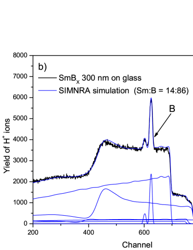
RBS studies were performed with the aim to determine an exact composition and thickness variation of the prepared thin films. He+ ion beam incoming angle of 0∘ and 45∘ were used to increase significantly the depth resolution, thus to see quality of the surface and interface. The results for 300 nm film presented in Fig. 1a are taken from 0∘ geometry. The studied films didn’t exhibit any differences, when evaluating the spectrum collected under the perpendicular and glancing geometry, or the uncertainties were in the range of RBS precision. Evaluation of the spectra of the prepared thin film samples using SIMNRA software gave the B:Sm ratio between 85.5:14.5 (5.9) and 86.5:13.5 (6.4), i.e. 86:14 averaged ratio (truncated with regard to method precision). With the aim to increase sensitivity of light element (boron) detection also analogous RBS studies using H+ beam were performed (see Fig. 1b). SIMNRA simulation of the spectra (using the same parameters as for He+ ion beam) gave exactly the same (86:14) ratio of B:Sm. The same composition gained from two RBS experiments with different relative sensitivity to boron, represents confirmation that the prepared samples can be considered as stoichiometric SmB6 thin films (within experimental uncertainty of RBS).
Having found the right conditions for the PLD process, depositions of the SmB6 thin films on several different substrates, namely MgO, sapphire, and (not polished) ultra-low expansion GC were done. With the aim to obtain crystalline material, now the temperature of the substrates was kept at 600 ∘C which was the maximum achievable value in the used PLD apparatus. To be able to verify effect of the substrate temperature on the electrical characteristics, also the film on the GC substrate kept at ambient temperature was prepared. The depositions were done with the wavelength of 532 nm at pulse frequency of 2 Hz, and pulse energy of 59 mJ. The deposition rate (determined by a quartz balance) was 0.32 Å/s. The film thickness estimated from parameters of deposition process was approximately 150 nm, except of the films on GC, where lower thickness is expected, because in this case roughly the same amount of SmB6 material covers larger area due to the non-polished surface.
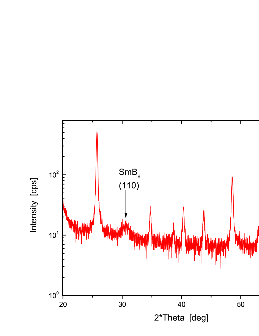
XRD studies were performed with the aim to obtain information about structural properties of the prepared films. Measurements of the films deposited on glass substrates at ambient temperature didn’t provide evidence for presence of any texture or crystalline phase. XRD profile of a sample deposited on polycrystalline GC at 600 ∘C is shown in Fig. 2. From analysis of this profile it can be deduced that the sample is nanocrystalline with mean grain diameter of about 4 nm and without any distinct texture, or the film can consist of nanocrystalline and amorphous phases. As can be seen in Fig. 2, only one (weak and broad) peak laying at the position of the strongest (110) peak for SmB6 was found in the XRD profile. The other peaks come from the substrate. Results for the sample deposited on GC at room temperature were similar.
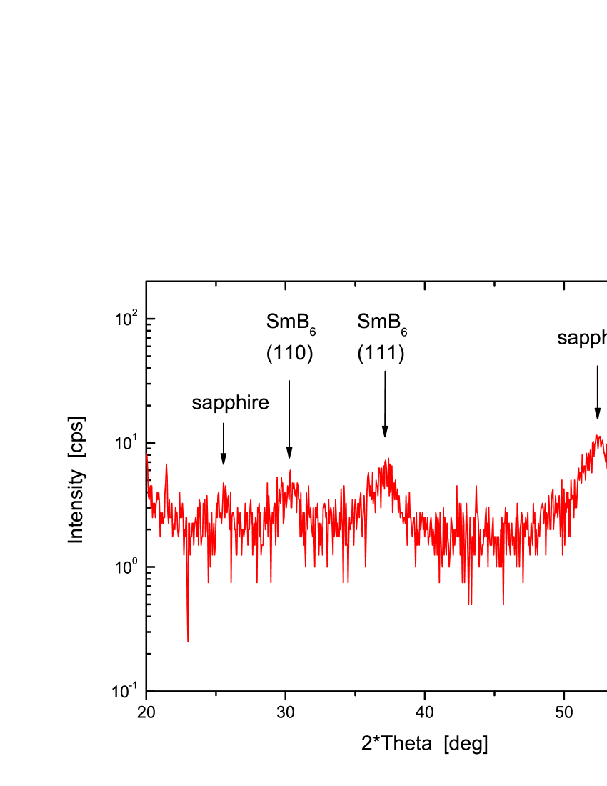
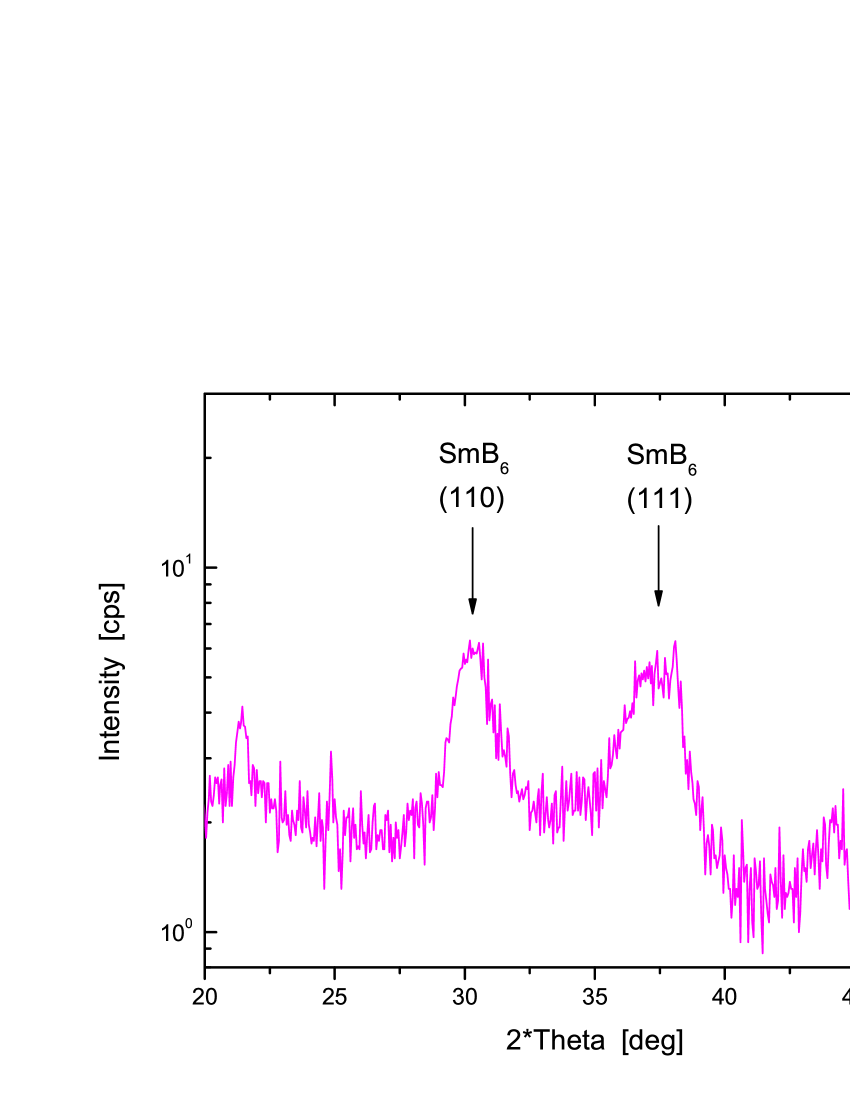
In accordance with expectations, measurements of the thin films deposited on single crystal substrates were strongly affected by a signal coming from the substrates, therefore we performed measurements of these samples utilizing Bragg-Brentano (BB) geometry and Grazing Incidence Diffraction (GID) geometry. Fig. 3 shows XRD profile of a sample deposited on sapphire for BB geometry. The profile reveals a peak which can be assigned to (100) peak for SmB6. The highest intensity peak in the XRD profile is (012) peak at 25,588 degrees, which is very weak such as sapphire substrate shows a miscut of about 1 deg. Two peaks (110) and (111) suggest also polycrystalline films. The XRD profiles shown in Fig. 4 were obtained in GID geometry (where an angle of x-ray incidence was equal to 3 deg); they confirm above mentioned suggestion, as broad and weak peaks laying at the positions of (110) and (111) peaks for SmB6 were found there. Unfortunately, we were not able to obtain reliable XRD results for films deposited on MgO as all detected peaks seemed to be connected with the substrate.
Electrical resistance of the SmB6 target was measured before deposition of the films with the aim to be able to compare it later with resistance of the deposited films. The measurement was performed from room temperature down to 4.2 K, while the target was fixed to a sample holder by a Teflon foil, and phosphor-bronze springs were used as electrical contacts. (Note that subsequent depositions were done from the side of the target which was not contacted.)

As shown in Fig. 5, normalized resistance 293 K) of the target reveals typical large resistance increase below 50 K. The ratio (5 K K) is more than two orders of magnitude lower than for high quality single-crystalline samples [6, 7, 22], which has been, however, expected due to larger contribution of surface states in polycrystalline materials and less purity of the used target material (99.5 %) in comparison with high-quality single-crystalline samples.
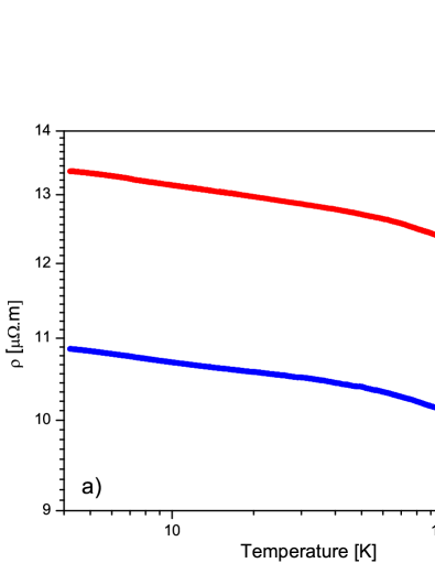
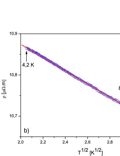
As can be seen in Fig. 6a, electrical resistivity of the films deposited on glass (at ambient temperature) increases with temperature decrease, but the largest increase is observed above 50 K, although dominant resistivity increase for bulk SmB6 samples is expected below 50 K. The resistivity of the films is more than 3-times higher than the resistivity of bulk SmB6 single crystals [5] or (stoichiometric) thin films reported by other group [3]. Such properties can be a consequence of deviation from the stoichiometry, as well as of high structural disorder in the films (e.g. amorphous state). As already mentioned, X-ray scattering studies haven’t provided any evidence for presence of texture or crystalline phase(s) in these films, thus supporting the supposition about structural disorder. With respect to the theory for disordered metals and heavily-doped semiconductors, which considers effects due to disorder and correlation [23], temperature dependence of the resistivity at lowest temperatures can be reasonably expected in the form , where parameter has negative value, as the contribution to the resistivity due to disorder and correlation effects increases with temperature decrease. Indeed, the plot of the resistivity data in vs coordinates, shown in Fig. 6b reveals that electrical resistance below 9 K can be described by law, what we consider as additional indication for presence of structural disorder.
As can be seen in Fig. 7, normalized electrical resistance 293 K) of the SmB6 thin films deposited on substrates kept at 600 ∘C behaves as expected for SmB6, i.e. exhibits significant resistance increase below 50 K, and has the tendency to saturate at lowest temperatures.
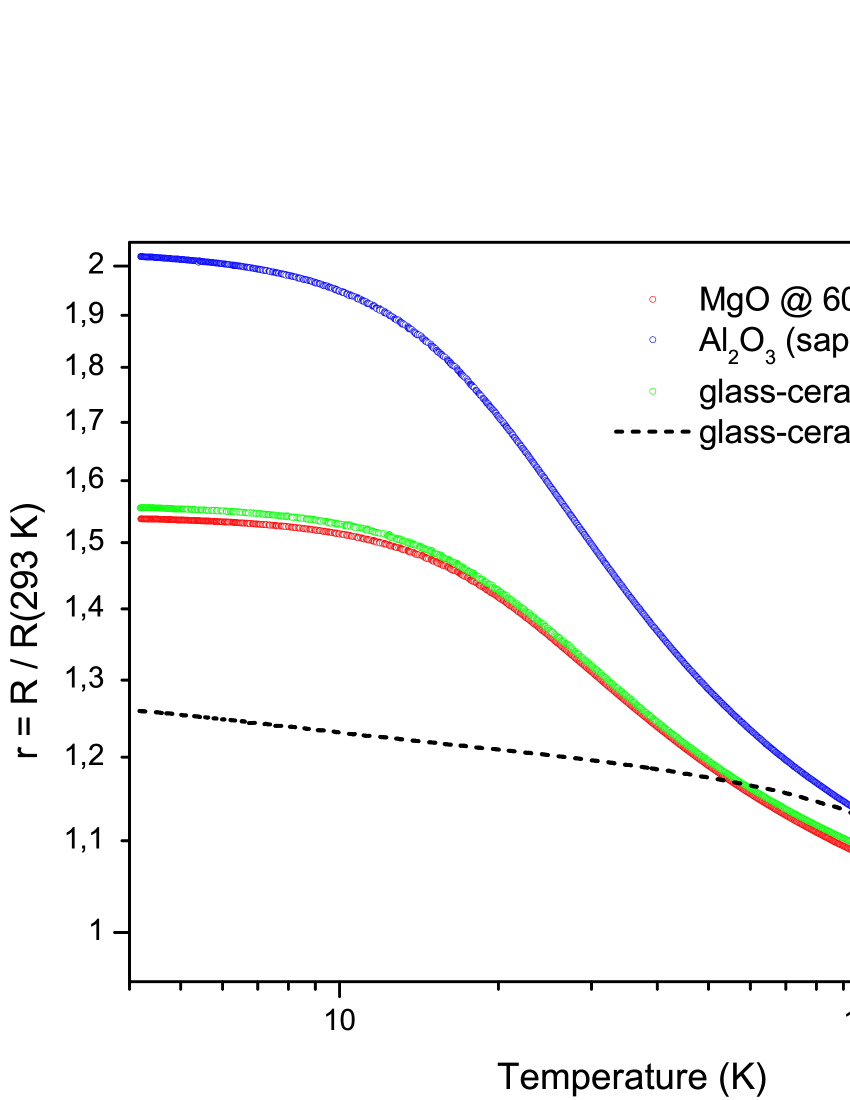
On the other hand, the curve of the thin film deposited on the GC substrate kept at the ambient temperature reveals a different dependence, which is, however, qualitatively the same as one for the films deposited at the ambient temperature on glass substrates, shown in Fig. 6. This confirms that heating the substrate during the deposition is crucial to obtain crystalline SmB6 thin films revealing electrical properties as typical for SmB6, while 600 ∘C is sufficiently high temperature. As can be moreover seen in Fig. 7, the normalized resistance is significantly influenced by the substrate material. The obtained values of 4.2 K) are 2.02, 1.56, and 1.54 for sapphire, GC, and MgO substrate, respectively. Comparing crystal structures, it seems surprising that the value of K) for MgO substrate is less than for sapphire, because the crystal structure and lattice parameters of MgO are much similar to ones of SmB6 in comparison to sapphire; MgO crystallizes in cubic structure, analogously as SmB6, with the lattice parameter = 4.216 Å at room temperature, which is very close to that of SmB6, 4.13 Å[24], while sapphire has hexagonal crystal structure with lattice parameters = 4.77 Å and = 13.04 Å. It seems that different thermal expansion of individual substrates play more important role in infuencing the properties of the prepared SmB6 thin films. Linear expansion coefficient of sapphire (perpendicular to c axis) at room temperature (/K) is less than that of MgO (K), and is close to one of SmB6, which is approximately K at room temperature, and reaches negative values at low temperatures, at least in the temperature range of 12 - 80 K [24]. Therefore, properties of SmB6/MgO thin films at room temperatures are expected to be affected by in-plane compressive residual strain induced after the deposition due to contraction of the substrate during cooling from 600 ∘C. It is generally known that application of hydrostatic pressure to SmB6 results in insulator-to-metal transition, which is accompanied by a strong resistivity decrease with increasing pressure at the lowest temperatures [7, 25]. Thus, lower value of (4.2 K) for SmB6/MgO in comparison to SmB6/saphire thin films can be explained by greater (positive) linear expansion coefficient of MgO in comparison to that of saphire. In addition, consideration that the strain induced in the SmB6 films by MgO substrate increases with temperature decrease in a certain region below room temperature, allows also to explain a very shallow minimum in the resistivity observed in the vicinity of 270 K. Opposite effect of substrate on the deposited SmB6 films, namely in-plane tension is expected for GC substrate having ultra-low expansion coefficient (/K) at room temperatures, and negative one at lower temperatures [26], similar to that of SmB6 [24]. The thermal expansion coefficient of sapphire is at the closest to one of SmB6 and therefore SmB6 thin films on sapphire substrate are supposed to be at least affected by in-plane strains.
Let us focus on electrical properties at the lowest temperatures. As reported by many authors before, electrical resistivity data of SmB6 at low temperatures can be adequately described by the two-channel model of electrical conductivity [6, 7, 17, 28, 16],
| (1) |
where is Boltzmann constant, is activation energy of the bulk transport, and parameters and are constants characterizing contributions to the conductivity from the surface states and the bulk, respectively. With the aim to compare electrical properties of the SmB6 target and the thin films deposited from it we performed corresponding numerical analysis of the experimental data. Obtained normalized resistance of the target and representative thin films plotted in Fig. 5 and Fig. 7, respectively, were fitted over a temperature interval (the same one for all films and the target), where Eq. 1 can be reliably applied, and where huge temperature dependence of the normalized resistance of the target is observed. In accordance with Eq. 1, the data were fitted by the formula
| (2) |
where the first term represents temperature non-activated (metallic) contribution, and the second one is temperature activated term associated with the bulk. Plotting the data in coordinates versus (using specific value of fitting parameter for each individual sample) has provided straight lines in all cases, at least in the temperature interval of 16 - 22 K, as can be seen in Fig. 8. Moreover, almost the same slope is observed for all thin films deposited at 600∘C, as well as for the target. Activation energies , determined from the data are summarized in the Table 1 together with other characteristics of the films and the target. The obtained values of activation energies are in good agreement with results of other groups [5, 6, 7, 17, 16, 28, 22]
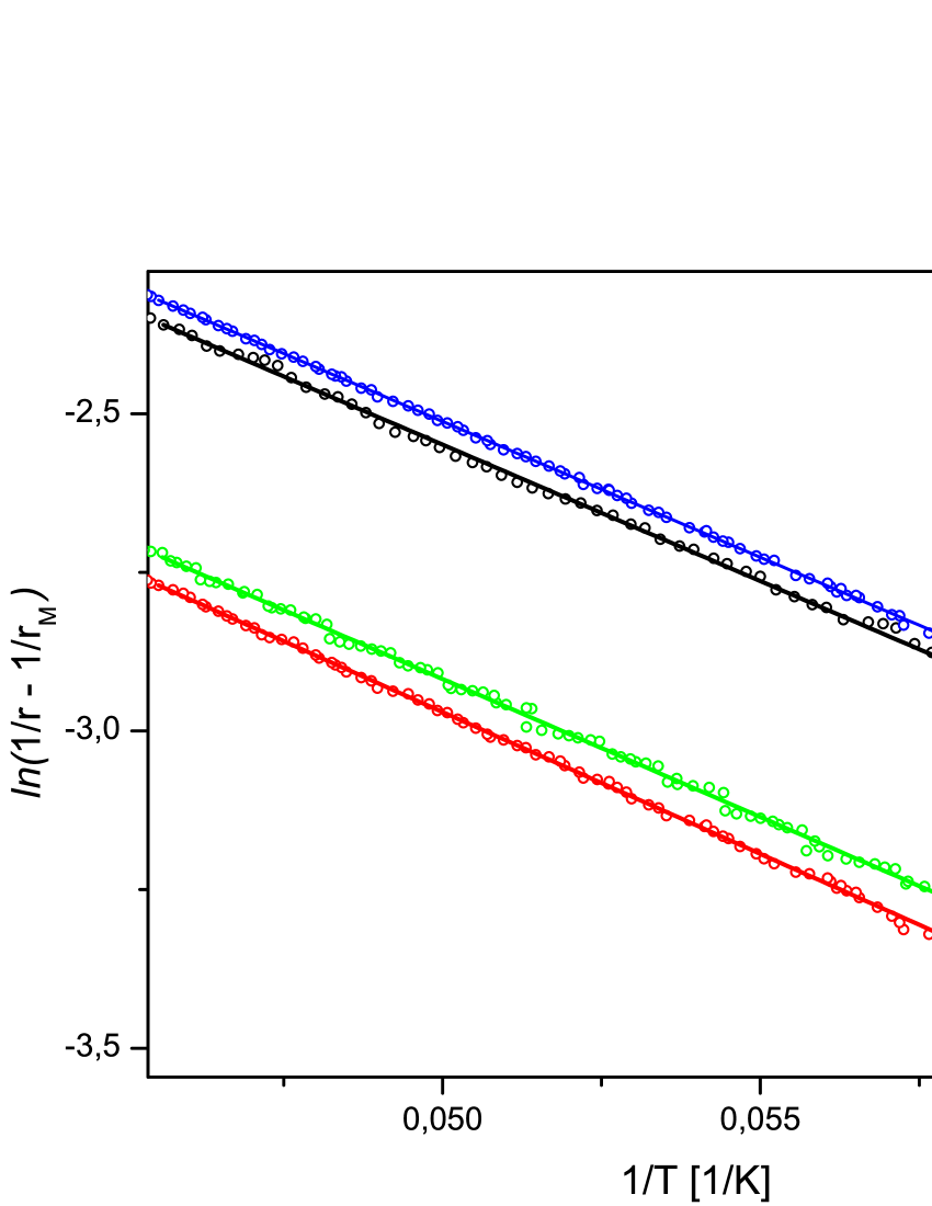
As follows from Tab. 1, the activation energy varies only weakly with the used substrate, and is very close to that of the target. This is a very important finding especially from technological point of view, because it reveals that bulk properties of the stoichiometric target material can be effectively transferred by the PLD process to the SmB6 thin films without need for additional boron source. Moreover, the bulk properties of the SmB6 thin films do not seem to be essentially affected by the properties of substrates. Considering the films deposited on sapphire and MgO (of almost the same thickness) one can expect that the bulk contributes to the total conduction by the same value. Thus, we suppose that observed differences in conduction are predominantly caused by different temperature independent contributions () due to different properties of the interface and/or different compressive or tensile strains induced changes in the near surface region, as both, compression [7, 25], as well as tensile strain [27] are parameters strongly affecting electrical properties of SmB6). In our opinion, the latter reason is more important, because of the fact that MgO lattice parameters are more similar to ones of SmB6, as discussed above.
| Sample | (4.2 K) | [meV] | 1/ | 1/ |
|---|---|---|---|---|
| Target | 59 | 3.70 | 0,023 | 0.670 |
| Sapphire | 2.02 | 3.69 | 0.504 | 0.690 |
| MgO | 1.54 | 3.82 | 0.654 | 0.479 |
| Clearceram®-Z | 1.56 | 3.75 | 0.647 | 0.447 |
Nevertheless, additional and more complex studies on wider series of SmB6 thin films are needed; here presented feasibility studies of reproducible grow of stoichiometric SmB6 thin films represent excellent starting information for their realization. As we have shown, PLD enables to prepare thin films with the composition and bulk properties that mirror ones of the used target. Hence, thanks to enabling synthesis of thin films of desired composition from a single composite or compound target corresponding to the desired composition of the films, the PLD can be very useful also for studies of doping or deviation from the stoichiometric chemical formula.
Also, utilization of PLD technique to deposit SmB6 (or SmB6-based) electrodes could enable (in combination with another deposition techniques, e.g. magnetron sputtering) fabrication of tunnel structures and consequent realisation of complex (planar) tunnelling spectroscopy studies of effect of composition on electronic properties of surface states in SmB6-based materials. In fact, mentioned approach could help to eliminate some technology problems arising in experiments if planar tunnel junctions are fabricated on the surface of SmB6 single crystals [29], and it could help to extend such studies also for composition similar (SmB6-based) materials, not (easily) achievable in a bulk-crystal form.
4 Conclusions
SmB6 thin films were successfully prepared by PLD from a single stoichiometric polycrystalline SmB6 target. It was demonstrated that using the right conditions of PLD, escape of boron can be avoided and there is no need for additional boron target. Performed RBS studies have shown that PLD process enables a growth of SmB6 thin films without any measurable deviation from the composition of the target. XRD studies provided indication that the prepared films are nano- or polycrystalline. Bulk electrical properties of the films very close to those of the target were reached by deposition on MgO, sapphire, and glass-ceramics substrates heated up to 600 ∘C. The highest ratio was observed for SmB6 films on sapphire, what we predominantly associate with the fact that thermal expansion parameter of sapphire is the closest to that of SmB6 in comparison to other used substrates. This might indicate preference of sapphire for potential applications. Also cost effective glass-ceramics substrates seem to be very promising alternative, because SmB6 films deposited on this substrate exhibit a higher resistance increase upon cooling in comparison with the films deposited on (frequently used) single crystalline MgO substrate.
5 Acknowledgments
This work was supported by the Slovak Scientific Agency VEGA (Grant No. 2/0015/17), by Czech Science Foundation (GACR No. P108/12/G108) and by European Regional Development Fund (ITMS 26110230097). The RBS studies were carried out at the CANAM (Centre of Accelerators and Nuclear Analytical Methods) infrastructure LM 2015056. M.B and I.B. thank L. Havela of Charles University in Prague for his helpful suggestions and valuable comments.
References
References
- [1] P. Wachter, Handbook on the Physics and Chemistry of Rare Earths, Vol. 19, North Holland, 1993.
- [2] P. S. Riseborough, Heavy fermion semiconductors, Advances in Physics 49 (2000) 257.
- [3] J. Yong, Y. Jiang, D. Usanmaz, S. Curtarolo, X. Zhang, L. Li, X. Pan, J. Shin, I. Takeuchi, R. L. Greene, Robust topological surface state in kondo insulator smb6 thin films, Applied Physics Letters 105 (22) (2014) 222403. doi:10.1063/1.4902865.
- [4] J. Yong, Y. Jiang, X. Zhang, J. Shin, I. Takeuchi, R. L. Greene, Magnetotransport in nanocrystalline SmB6 thin films, AIP Advances 5 (7) (2015) 077144. doi:http://dx.doi.org/10.1063/1.4927398.
- [5] J. W. Allen, B. Batlogg, P. Wachter, Large low-temperature Hall effect and resistivity in mixed-valent SmB6, Phys. Rev. B 20 (1979) 4807–4813. doi:10.1103/PhysRevB.20.4807.
- [6] I. Bat’ko, P. Farkašovský, K. Flachbart, E. S. Konovalova, Y. B. Paderno, Low temperature resistivity of valence fluctuation compound SmB6, Solid State Commun. 88 (1993) 405 – 410.
- [7] J. C. Cooley, M. C. Aronson, Z. Fisk, P. C. Canfield, SmB6: Kondo insulator or exotic metal?, Phys. Rev. Lett. 74 (1995) 1629 – 1632. doi:10.1103/PhysRevLett.74.1629.
- [8] M. Dzero, K. Sun, V. Galitski, P. Coleman, Topological Kondo insulators, Phys. Rev. Lett. 104 (2010) 106408. doi:10.1103/PhysRevLett.104.106408.
- [9] M. Dzero, K. Sun, P. Coleman, V. Galitski, Theory of topological Kondo insulators, Phys. Rev. B 85 (2012) 045130. doi:10.1103/PhysRevB.85.045130.
- [10] F. Lu, J. Zhao, H. Weng, Z. Fang, X. Dai, Correlated topological insulators with mixed valence, Phys. Rev. Lett. 110 (2013) 096401. doi:10.1103/PhysRevLett.110.096401.
- [11] V. Alexandrov, M. Dzero, P. Coleman, Cubic topological Kondo insulators, Phys. Rev. Lett. 111 (2013) 226403. doi:10.1103/PhysRevLett.111.226403.
- [12] Z.-H. Zhu, A. Nicolaou, G. Levy, N. P. Butch, P. Syers, X. F. Wang, J. Paglione, G. A. Sawatzky, I. S. Elfimov, A. Damascelli, Polarity-driven surface metallicity in SmB6, Phys. Rev. Lett. 111 (2013) 216402. doi:10.1103/PhysRevLett.111.216402.
- [13] I. Batko, M. Batkova, SmB6: Topological insulator or semiconductor with valence-fluctuation induced hopping transport?, Solid State Commun. 196 (2014) 18.
- [14] X.-L. Qi, S.-C. Zhang, Topological insulators and superconductors, Rev. Mod. Phys. 83 (2011) 1057–1110. doi:10.1103/RevModPhys.83.1057.
- [15] M. Z. Hasan, C. L. Kane, Colloquium, Rev. Mod. Phys. 82 (2010) 3045–3067. doi:10.1103/RevModPhys.82.3045.
-
[16]
M. Shaviv Petrushevsky, P. K. Rout, G. Levi, A. Kohn, Y. Dagan,
Signature of surface state coupling in thin
films of the topological kondo insulator SmB6 from anisotropic
magnetoresistance, Phys. Rev. B 95 (2017) 085112.
doi:10.1103/PhysRevB.95.085112.
URL 10.1103/PhysRevB.95.085112 - [17] P. Syers, D. Kim, M. S. Fuhrer, J. Paglione, Tuning bulk and surface conduction in the proposed topological Kondo insulator SmB6, Phys. Rev. Lett. 114 (2015) 096601. doi:10.1103/PhysRevLett.114.096601.
- [18] H. Shishido, Y. Yoneda, T. Yoshida, S. Noguchi, T. Ishida, Semi-epitaxial SmB6 thin films prepared by the molecular beam epitaxy, Physics Procedia 75 (2015) 405 – 412.
- [19] K. Jin, R. Suchoski, S. Fackler, Y. Zhang, X. Pan, R. L. Greene, I. Takeuchi, Combinatorial search of superconductivity in fe-b composition spreads, APL Materials 1 (4) (2013) 042101. doi:10.1063/1.4822435.
- [20] I. Bat’ko, K. Flachbart, J. M. J., V. M. Filipov, E. S. Konovalova, Y. B. Paderno, Electrical resistivity of smb6 thin films, Journal of the Less Common Metals 158 (1990) L17 – L19.
- [21] M. Mayer, SIMNRA User’s Guide, Tech. Rep. IPP 9/113, Max-Planck-Institut für Plasmaphysik, Garching, 1997.
- [22] M. Batkova, I. Batko, E. S. Konovalova, N. Shitsevalova, Y. Paderno, Gap properties of SmB6 and YbB12: Electrical resistivity and tunnelling spectroscopy studies, Physica B 378 - 380 (2006) 618.
- [23] B. L. Altshuler, A. G. Aronov, Contribution to the theory of disordered metals in strongly doped semiconductors, Solid State Commun. 30 (1979) 115.
- [24] D. Mandrus, J. L. Sarrao, A. Lacerda, A. Migliori, J. D. Thompson, Z. Fisk, Low-temperature thermal-expansion of SmB6 - evidence for a single-energy scale in the thermodynamics of Kondo insulators, Phys. Rev. B 49 (1994) 16809 –16812. doi:https://doi.org/10.1103/PhysRevB.49.16809.
- [25] S. Gabáni, E. Bauer, S. Berger, K. Flachbart, Y. Paderno, C. Paul, V. Pavlík, N. Shitsevalova, Pressure-induced Fermi-liquid behavior in the Kondo insulator SmB6: Possible transition through a quantum critical point, Phys. Rev. B 67 (2003) 172406. doi:10.1103/PhysRevB.67.172406.
- [26] Ultra-low expansion glass-ceramics CLEARCERAM®-Z, http://www.oharacorp.com/pdf/ccz-2013-nav.pdf, accessed: 2017-06-05.
- [27] A. Stern, M. Dzero, V.M. Galitski, Z. Fisk and J. Xia, Surface-dominated conduction up to 240 K in the Kondo insulator SmB6 under strain, Nat. Mater. 16 (2017) 708. doi:https://doi.org/10.1038/nmat4888.
- [28] S. Wolgast, C. Kurdak, K. Sun, J. W. Allen, D.-J. Kim, Z. Fisk, Low-temperature surface conduction in the Kondo insulator SmB6, Phys. Rev. B 88 (2013) 180405. doi:10.1103/PhysRevB.88.180405.
- [29] L. Sun, D.J. Kim, Z. Fisk, W.K. Park, Planar tunneling spectroscopy of topological Kondo insulator SmB6, Phys. Rev. B 95 (2017) 195129. doi:10.1103/PhysRevB.95.195129.