Charged exciton kinetics in monolayer MoSe2 near ferroelectric domain walls in periodically poled LiNbO3
Abstract
Monolayers of semiconducting transition metal dichalcogenides are a strongly emergent platform for exploring quantum phenomena in condensed matter, building novel opto-electronic devices with enhanced functionalities. Due to their atomic thickness, their excitonic optical response is highly sensitive to their dielectric environment. In this work, we explore the optical properties of monolayer thick MoSe2 straddling domain wall boundaries in periodically poled LiNbO3. Spatially-resolved photoluminescence experiments reveal spatial sorting of charge and photo-generated neutral and charged excitons across the boundary. Our results reveal evidence for extremely large in-plane electric fields of 3000 kV/cm at the domain wall whose effect is manifested in exciton dissociation and routing of free charges and trions toward oppositely poled domains and a non-intuitive spatial intensity dependence. By modeling our result using drift-diffusion and continuity equations, we obtain excellent qualitative agreement with our observations and have explained the observed spatial luminescence modulation using realistic material parameters.
keywords:
Two-dimensional semiconductor materials; transition metal dichalcogenides; acoustic interlayer breathing modes; ultra-fast time-resolved spectroscopy; phonon dynamics; phonon lifetimeDepartment of Materials Science and Engineering, Massachusetts Institute of Technology, Cambridge, Massachusetts 02139, USA
For integrated opto-electronic and quantum photonic devices, the ability to combine different materials having complementary functionalities is key to achieving high performance. Two-dimensional (2D) transition metal dichalcogenides (TMDs), having the chemical formula MX2 (M=Mo,W and X=Se,S), are of strong current interest since they are direct gap semiconductors in the monolayer form, with bandgaps that are tunable throughout the visible spectral range. They host strongly bound excitons (Bohr radii -nm, binding energy -500 meV) 1 that remain stable up to room temperature 2. Moreover, they can be readily van-der-Walls bonded onto a wide range of different substrates 3. Unlike conventional semiconductors, the atomic thickness and 2D nature of TMDs is such that their properties change depending on the substrate onto which they are placed. This opens up new routes to tailor the exciton energy landscape by intentionally placing TMDs onto substrates with spatially varying dielectric properties 4, 5, 6, 7, 8. For example, lateral quantum confinement can enhance quasiparticle correlations, opening the way to study collective behaviour and many-body physics 9, 10, 11, 12, 13, 14, 15.
While dielectric engineering is sufficient for trapping neutral excitonic complexes, the manipulation of free-charges and charged excitons and the exciton ionization needed for efficient photodetection requires strong electric fields 16, 17, 18, 19. Gate tunable devices with e.g. nanoscale metallic contacts can result in strain fields and large Schottky barrier heights. Moreover, proximity-induced electric fields arising from Fermi-level pinning produce band bending and local potential barrier in the TMD 18, 20. As such, new approaches are needed to produce high electric fields over lengthscales comparable to the exciton Bohr radius. Lithium niobate is an exceptional material for integrated opto-electronics and photonics; it has a broad transparency window spanning the range 0.35-5 m, strong optical activity that can enable optical phase modulation as fast as 100 GB/s 21, 22, 23 and can be integrated on oxide sacrificial layers using CMOS compatible processes to produce low loss waveguides (dB/m 24). Moreover, periodically poled lithium niobate (PPLN) is ferroelectric 25, 26, 27 and has extremely large in-plane surface charge densities within individual domains 28, 29. Atomically sharp ferroelectric interfaces (domain walls) in combination with the insulating nature of PPLN, result in extremely intense in-plane electric fields 30, capable of driving e.g. localized photochemical reactions 31, 32 and ferroelectric lithography of multicomponent nanostructures 33. Furthermore, the size and shape of such domains can be freely tailored during the ferroelectric pattering 25, 26, 27, 34. Placing TMD monolayers and heterostructures onto ferroelectric materials provides the possibility to locally tune optical 25, 26, 27, 35 and electronic properties 27, 36, 37, engineer the local charge density landscape 25 and facilitate study of fundamental properties such as in-plane exciton polarizability and dissociation 38, 39.
Here, we explore the excitonic photo-physics of monolayer MoSe2 exfoliated onto a PPLN crystal. By performing low-temperature ( K) micro-photoluminescence (PL) measurements, we observe separation and localization effects of charged excitons and free carriers in the flake close to the domain wall (DW) between positively () and negatively () poled ferroelectric domains, orientated perpendicular to the PPLN surface. Due to the very large in-plane electric fields that form at the ferroelectric DW boundaries 30, free-charges and photogenerated charged excitons respond to the DW by forming a characteristic charge and photo-generated texture. In addition, we observe that the DW induces strong modulation of the relative energies of the neutral and charged excitons in the monolayer MoSe2. We theoretically model our observations using drift-diffusion and continuity equations 40, 41 and find excellent qualitative agreement with our experimental results. Our simulations allow us to evaluate the dynamics of charged carriers in the system and show that the combined structure of DW and MoSe2 behaves like a nanometer scale lateral p-n homojunction. These results are an important step towards integrated optoelectronic devices utilizing atomically thin semiconductors on PPLN and provide new insights into the excitonic photophysics subject to very large electric fields.
1 Results and Discussion
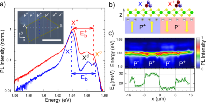
We recorded PL data with an optical CW power of W (eV) focussed to a diffraction limited spot (100x objective, NA=0.7). Figure 1a shows a typical spectrum obtained well within (blue) and (red) domains. The inset of figure 1a shows an optical micrograph recorded from the studied sample. The picture shows the monolayer thick MoSe2 crystal outlined by the yellow line and the DWs are denoted by grey vertical lines. The sample is exfoliated onto the PPLN substrate such that the monolayer spans multiple domains. For details of how we determined the PPLN domains, see the Additional Information 42. The spectra presented are the spatially averaged spectra along vertical blue and red transects illustrated by the dotted lines in the inset. Within both domains we observe emission close to eV, consistent with other reports 43, 44. However, in both domains the dominant emission feature arises from trions; around eV 43, 44. In addition, we observe a luminescence peak at eV, labelled on Fig. 1b, which does not occur when the same crystal is exfoliated onto SiO2 or hexagonal boron nitride. We identify this peak as arising from defect induced transitions 45 and do not discuss it for the remainder of this manuscript. The electric polarization of the LN () in a direction normal to the plane of the MoSe2 monolayer (-axis) results in a large density of fixed surface polarization charges 26, as indicated in the schematic of Fig. 1b. These surface charges attract oppositely charged mobile carriers from the native doping of the monolayer and thus, at the center of each domain, a neutral exciton () can bind an available additional electron or hole to form positive () or negative () trions, respectively. The pronounced emission of trions is thus an evidence of a large accumulation of holes and electrons in the and and therefore, the PPLN creates an electronic landscape that is similar to a p-n junction.
We continue to explore the behavior of the steady state PL when spanning different domains in the MoSe2. Fig. 1c shows a series of spatially dependent PL spectra presented as a false color representation along the axis A-B, denoted by the white dotted line in the inset of Fig. 1a. The domains are clearly visible due to an enhanced background PL emission in the regions, possibly due to negatively charged chalcogen vacancies in the material 19, 25, 44, 46, 45, 47, 48. Most prominently, the energy of both and trion peaks (eV) shifts abruptly across the interface, while simultaneously, the energy of the neutral exciton shifts in the opposite direction to the trion. Hence, the binding energy of the trion ( 19) changes abruptly across the DW interface. We quantify the change of by fitting the PL spectra and statistically analyzing the relative peak positions across the domains. The results of this analysis are plotted in the bottom panel of Fig. 1c, which shows a clear modulation of induced by the different polarization states in the PPLN. As the binding energy of a trion is proportional to the effective masses of the individual particles of the bound state (e.g. , where is the electron mass and is the hole mass) 19, 49, 50, 51, 52, we attribute the variation in to the different charge of the trions on each side of the interface. Consistent with literature 25, we find that the domains feature , while in the domains we predominantly observe emission. The modulation in occurs abruptly within the step size of our lateral scanning stage, nm. Such abrupt modulations of the neutral exciton binding energy have been realized in monolayer TMDs by encapsulation 12, however here we do not modulate the dielectric environment of the system, but rather spatially modulate the local charge density in the TMD monolayer via the PPLN surface charge. The sharp modulation in is an indication that the electric field gradient across the DW is very large, as discussed in detail below.
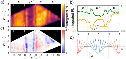
We now focus our analysis on the effect of the PL intensity close to the DW. Even though the modulation of the spectrally integrated PL intensity and is a direct consequence of the underlying domain structure, they show different behaviour. As can already be seen in the raw spectra plotted in Fig. 1c, the PL intensity is modulated on both sides of the interface, while the modulation in follows a step-like pattern. Figure 2a presents a map of the total integrated PL across the sample. It shows that the PL intensity reflects the geometry of the underlying DW boundaries in the -direction, but also that satellite stripes of intensity are observed orientated along the -direction, positioned m away from the DW boundary.
To elucidate this unexpected behavior, we plot in Fig. 2b the averaged total intensity integrated over the spectral range of the and emission as a function of the -position of the laser spot. On either side of the DW boundary, we observe that the charged exciton emission increases while simultaneously, the neutral exciton emission decreases in an anticorrelated manner. This behavior in combination with the step like modulation is consistent with an increase in the electron and hole density on each side of the interface that facilitates the formation of positive and negative trions and reduces the local formation probability for . Thereby, the electric field across the ferroelectric DW, which has a thickness of few nanometers 53, promotes the dissociation of excitons and the separation of trions in a micrometer scale according to their charge species.
The separation of positive and negative trions along the macroscopic PPLN DW is presented in Fig. 2c, and is one of the main experimental findings of this letter. In this map, we colour code the trion intensity based on the fact that meV and meV (Fig. 2d). Trion intensities at energies below (above) 28.5 meV are presented in red (blue) scale to highlight their different charge species. In the center of each ferroelectric domain, the induced electric field is oriented in the direction of its polarization (-direction). However, the separation of charged excitons in a direction defined by the sign of their charge is a clear fingerprint of an in-plane electric field perpendicular to the interface, along the -direction. Such an electric field is provided by the formation of a Néel-type DW 53, 28 as depicted in Fig. 2d. As consequence, optically-generated electron-hole pairs are dissociated and the resulting free carriers are efficiently separated by the DW. In our experiment, we scan the diffraction limited laser focal volume at a position across the sample and detect the PL from the same spot. Nevertheless, due to the strong in-plane electric fields, specifically at the DW, the exciton generation as well as the drift and diffusion of charged excitons and excess carriers is strongly dependent on . The complete process is illustrated schematically in figure 3a.
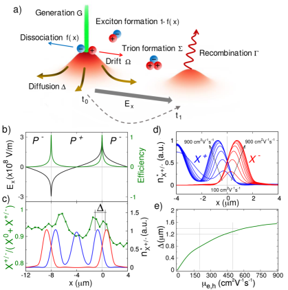
By solving a closed set of coupled differential equations that include the optical generation, exciton and trion formation, drift and diffusion, we qualitatively describe the time evolution of the different particle densities until they reach the steady state. Details of our approach can be found in the Additional Information 42. Typical results are presented in figure 3. Figure 3b shows the spatial in-plane electric field profile experienced by the MoSe2 monolayer at the surface of the PPLN substrate. In this calculation, we use a uniform fixed positive and negative charge density of Cm2 in the domains, in accordance with the charge density deduced from the modulation of the refractive index of the material, as shown in the Additional Information 42. The calculated electric field strength at the interface is extremely high, of 3000 kV/cm and comparable to the breakdown field of hexagonal boron nitride 56. This opens the possibility to perform the experiments shown here in a gate-tunable device made from stacked van der Waals materials. As the energy of free carriers exposed to the electric field has to overcome the large exciton binding energy in the monolayer MoSe2, we model the probability of exciton dissociation, (see Fig. 3b), 1.
With the in-plane electric field and the generation efficiency as input in our coupled rate equations (Figs. 3b), we calculate the steady state of the different particle distribution and obtain, in this way, their spatial density profile across the PPLN domains as the laser spot is scanned across the sample. The spatial redistribution of luminescence intensity along the PPLN domain edges is due to the spatial density profile of excitons and trions. Since the equations are highly interdependent and sensitive to material properties, here we only focus on the dependence on carrier mobility, while additional more detailed information is presented in the Additional Information 42.
Figure 3c presents the calculated spatially dependent density of , , and compares it to the relative PL intensity profile of excitons and trions. The symbol denotes that we plot the observed density as the laser spot is scanned across the sample (see ref. 42). The simulation clearly shows that we can quantitatively describe the separation of charged excitons at the interface as observed in the experimental data of Fig. 2. Positive excitons form predominantly on the side at the interface, but not at the DW boundary. In comparison, negatively charged trions form in the opposite side of the DW (see Fig. 2c). The increase of the intensity towards the center of the domain is controlled by the native electron doping of MoSe2, described above. Since the charge mobility depends on the effective mass and our results for the and binding energy supports the conclusion of similar effective electron and hole masses, we use an equal carrier mobility for both particles. In figure 3d, we show the spatial distribution of density in the vicinity of the interface for a range of carrier mobilities. For a given electric field, free charges and trions (, and ) are accelerated large distances away from the DW, an effect that defines the spatial position of the peak of the calculated distribution at the DW. The highly nonlinear amplitude of with excitation power is the result of a delicate interplay of electron/hole generation, drift, diffusion and exciton formation probability close to the interface (see Additional Information 42). We deduce and plot the separation of the -luminescence peak () in Fig. 3e and find that the experimentally measured peak separation agrees well with our calculated values using a carrier mobility of cm2V-1s-1. This value is in very good accord to previously published values for MoSe2 at low temperatures 54. Remarkably, despite its simplicity our model qualitatively describes the relevant physics in this system, although we reiterate that the formation and recombination of excitons is a highly non-linear process that depends on several interralated material specific parameters.
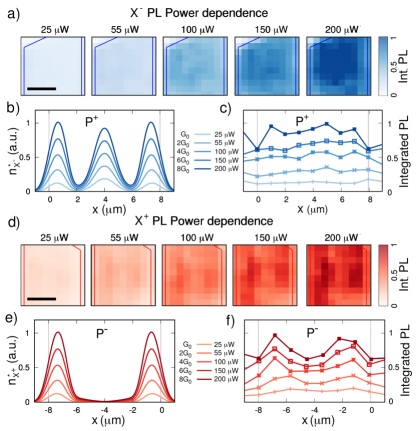
To further explore the consistency of the implemented model, we evaluate the PL dependence with the laser power from to W. Over the studied range, the intensity of shows a monotonic increase and therefore confirms that we probe the sample in a regime where saturation effects due to exciton-exciton annihilation are not significant. Figure 4a shows a sequence of color maps of the integrated PL intensity recorded for increasing excitation levels. In the domain, the PL intensity is spatially homogeneous along the -direction. Variations in the total intensity along the -direction may be related to varying contact of the MoSe2 to the substrate and edge effects. Figures 4b and c present the modeled density and the experimental PL intensity along the -direction for increasing generation rate of excitons and laser power, respectively. Once again, we find a linear dependence with increasing optical power, in a similar fashion as before.
As indicated above, the calculated and measured luminescence intensity across the domain is distributed close to the DW but also in the center due to the native electron density in the MoSe2 layer. Although the calculated density is not uniform across the -direction, it nicely reproduces the presence of negative trions in the center of the domain with an intensity that, in this regime, is also directly proportional to the generation rate. The lack of negative trion stripes close to the DW is most likely due to the limited spatial resolution of m in our experiment. Figures 4d-f show the analogous dependencies of the integrated PL intensity for the on power and position. The significant difference with the case is the obvious spatial variation of the intensity across the domain, due to the concentration of the close to the interface and the lack of native charge doping in the center of the domain. Moreover, we reiterate that our simple calculations capture the salient photophysics in our experiments. The model can be improved to further enhance the agreement with the experimental results by introducing, for instance, electron-electron interactions that would take into account the electric field screening 57, 58, providing a more uniform and intense negative trion density in the center of the positive domains. Such approaches are, however, beyond the scope of our model.
In summary, we observe clear evidence for the impact of surface polarization charges and local electric field gradients on the excitonic photophysics of monolayer MoSe2 placed on PPLN. The ferroelectric domains separate and localize charged excitons according to their charge species. The impact of the surface polarization charges due to the PPLN is observed in spatially resolved PL experiments by analysing the spectral position of exciton and trion emission. We modelled our findings using a self-consistent generation, drift-diffusion finite element model and obtained results that were in excellent qualitative agreement with our experiments. Our model is robust and can qualitatively describe the physics of charged exciton formation and spatial distribution by strong in-plane electric fields in the linear regime where exciton-exciton and electron-electron interactions are not relevant. The huge magnitude of the electric field set by the atomically flat PPLN substrate (3000 kV/cm) is difficult to reach using other techniques, such as gated devices since it can easily cause the dielectric breakdown of the system. On the other hand, even when this issue may be solved by means of hBN encapsulation, the metallic contacts generate a depletion region in the electronic bands of the TMD that hinder the localization of the charged particles in small regions 20, 18. Under these considerations, PPLN represents a highly interesting platform to manipulate and localize charges in TMDs, and paves the way towards integrated photonic structures and waveguides that combines LiNbO3 and 2D materials.
2 Methods
Sample fabrication. The ferroelectric domain arrays were fabricated by bulk electric-field poling of 500 m-thick congruent -cut LiNbO3 34. The poling pattern was defined by means of periodic openings in a micrometer-thick photoresist mask (S1818) deposited on LiNbO3 monodomain samples. The PPLN pattern consisted of 15 uniform bands of constant period (), ranging from 14.5 to 16.5 m, in steps of 0.5 m. Local domain switching was performed at room temperature, by applying 60 ms pulsed electric fields exceeding the LiNbO3 coercive value (21 kV/mm), with a uniform electrical contact on the face and periodic liquid electrode contacts through the openings of the photoresist on the face. After poling, the poling mask was removed by ultrasonic rinsing the samples in deionized water, acetone and isopropanol and N2 blow-drying. The resulting 1D ferroelectric arrays exhibited a periodic pattern with domains of alternating polarity () along the crystallographic -axis and with atomically-thin 250 m-long DWs aligned to the -axis. Finally, monolayer MoSe2 was transferred onto the PPLN substrate by the dry viscoelastic transfer method 59 such that the monolayer covered several PPLN domains.
PL experiments. All the photoluminiscence experiments where performed using a confocal microscope foccused to the diffraction limited spot of 0.7 m on the sample with a photon energy of 1.96 eV ( nm, HeNe laser). During the experiments the sample was kept at K and the continuous wave excitation power was 20 W unless otherwise noted. For the statistical analysis of the PL spectra, we omitted data recorded within m distance to flake edges to avoid well known edge effects (defects, strain, etc.).
We gratefully acknowledge the German Science Foundation (DFG) for financial support via the clusters of excellence e-conversion (EXC 2089) and the Munich Center for Quantum Science and Technology (MCQST, EXC 2111). Moreover, we gratefully acknowledge the DFG Priority Programme (SPP 2244) via FI 947/7-1, the BMBF project QuaDiQua and the Alexander von Humboldt Stiftung for support. K.G. gratefully acknowledges support from the Wallenberg Centre for Quantum Technology and the Swedish Research Council (VR) through grants no. 2018-04487 and 2016-06122.
Competing financial interests
The authors declare no competing financial interest.
3 Additional Information
3.1 Determination of the PPLN domains and in-plane electric field estimation
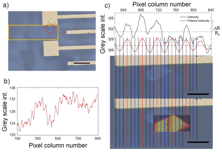
Figure 5a presents an optical micrograph of the sample taken with a 20 objective. The light coloured structure correspond to metallic contacts used to ground the sample and avoid its electrostatic doping. In this figure, vertical dark and bright stripes can be clearly identified, corresponding to intensity variations of the reflected light in the substrate due to different ferroelectric domains. The red circle in the figure indicates the region in which the monolayer MoSe2 flake is located and the yellow rectangle limits the region selected to post process the picture by vertically averaging the pixel gray scale intensity. As the horizontal intensity alternation pattern is not observed in optical micrographs taken with higher magnification objectives, in order to identify the DW in the monolayer it was necessary to process this optical image and combine it with optical images taken with higher magnification objectives. The pixel intensity variations are presented in Fig. 5b. The upper panel of figure 5c shows an enlargement of the curve in b in the region of the monolayer, and the band-pass filtered data. The central panel presents the overlap of optical images taken with 20 100 objectives and the lower panel overlaps to this picture the integrated total PL intensity map. The blue, black and red vertical lines indicate the position of minima, zeros and maxima of the filtered signal in the upper panel, respectively. By direct inspection between the different regions in the PL map with the maxima and minima of the grey scale curve (red and blue vertical lines), it is possible to find that the pixel intensity oscillations are out of phase with respect to the different PL intensity regions. In other words, the extremes of the reflectivity curve coincide with the DWs and not with the center of each ferroelectric domain. This observation is consistent with the existence of an in-built electrostatic field at the DW, that modulates the refractive index of the PPLN due to Pockels effect 60.
The refractive index modulation amplitude can be directly inferred from the variation in the grey scale intensity retrieved from the optical micrograph. Specifically, assuming that the grey scale pixel intensity is proportional to the reflectivity of the PPLN () and applying the Fresnel equations, we get
| (1) |
where is the proportionality constant and is the spatially-varying refractive index, oscillating around the unperturbed value, corresponding to the ordinary refractive index of LN, , with an amplitude due to the Pockels effect perturbation. A first order expansion of this expression provides the relationship between and :
| (2) |
From figure 5c and equation 3.2 it is possible to estimate , , and . From this expresion, an estimate of the in-plane electrostatic field at the domain wall can be obtained by combining equation 3.2 with the expected variation of the refractive index at a Néel DW due to the Pockels effect. Tensorial derivations for the electro-optic effect at the domain wall, accounting for the Néel rotation of the LN electro-optic tensor 28, assuming an in-plane depolarization electrostatic field () oriented along the -axis (i.e. orthogonal to DW) and considering only the dominant contribution of the largest electro-optic coefficient of LN (), ultimately result in the following scalar relationship between the in-built electric field and the index variation at the domain wall:
| (3) |
where is the refractive index of the material in the absence of , i.e. the ordinary refractive index of LN, and m/V its electro-optic coefficient. By combining equations 3.2 and 3.2 we obtain an estimate of the in-plane electric field kV/cm, which was used as input in the calculation of the electric field by finite elements presented in the main manuscript. It is important to highlight that to reach an in-plane electric field with this strength it was necessary to introduce in the calculations a charge density of C/m2.
3.2 Drift-diffusion continuity equations
The incidence of a laser beam over the 1L-MoSe2 flake generates electron-hole pairs in the TMD whose kinematics is strongly influenced by the PPLN. At the center of the different domains, where is weak, these electron-hole pairs can easily form an exciton. However, at the DW, where has a large intensity, electron-hole pairs are dissociated and the resulting free carriers are efficiently separated towards opposite ferroelectric domains. In this way, the raise of the charge landscape in each domain facilitates the formation of trions and reduces the density of neutral excitons. We quantify the modulation of the particle densities across the PPLN domains with a set of five coupled differential rate equations that describe, in time, the generation, recombination, drift and diffusion of electrons, holes as well as neutral and charged excitons in a 1D toy model 40, 41. For neutral excitons, the rate equation can be written as
where an exciton density is generated via the generation rate of intensity and a Gaussian shape at position . This function describes the effect of the finite Gaussian beam, while the efficiency of this generation, , depends on the position on the sample. For example, directly at the boundary, this efficiency tends towards , since excitons are immediately dissociated due to the large in-plane electric field 61, 62, 63. The excitons diffuse away from their generation spot, described by the diffusion equation with the diffusion constant . Across the sample, there is a remaining electron and hole density (), such that an exciton can capture a charged particle and form negatively (positively) charged excitons at a rate (). Finally, the neutral exciton recombines with the rate , where is the exciton lifetime.
Since the strong in-plane field at the DW dissociates excitons into free electrons and holes, the rate equations for excess charges in the 2D material can be written as
and
where the drift term for electrons and holes due to the in-plane electric field is . The recombination rate of charged excitons ( and ) is presented in these equations as an extra source of electrons and holes, respectively. Finally, the rate equations for positively and negatively charged excitons in the system are
In the latter equation, the source of trions is the term , equal to the rate in which an exciton captures a charge, and thus contributed negatively in the previous equations.
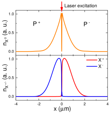
Figure 6 presents and generated by a Gaussian beam , centered at the DW and calculated with the set of equations presented above. In the upper panel, the exciton density shows a dip in its density at due to the huge electric field at the interface. The charged excitons are pushed out of the domain wall and are separated in different domains, as shown in the lower panel. Note that this system of equations describes the particles density distribution generated by the laser beam at a position . Nevertheless, only the density of particles that is in the region sensed by the laser beam is observed in the PL experiments. To obtain the observed distribution of particles for a laser at , as presented in the main text, it is necessary to spatially integrate these distributions multiplied by . For instance, the observed density of excitons and trions at is
and
respectively.
The complete set of parameters used in the calculations is presented in table LABEL:tb:par. Those material parameters that were not found in the literature were estimated so that they correlate with those that were found in the literature. Finally, the charge capture rates ( and ) were fitted to obtain an exciton-trion rate similar to those observed in the experiments.
| Gaussian spot diameter | 0.7 m | |
| Exciton diffusion | 14 cm-2s-1 (64, 65) | |
| Exciton lifetime | 100 ps (66, 65, 64) | |
| Native electron doping | cm-2 (19) | |
| Electron mobility | 500 cm2V-1s-1 (47) | |
| Electron difussion | 30 cm-2s-1 | |
| Hole mobility | 500 cm2V-1s-1 | |
| Hole difussion | 30 cm-2s-1 | |
| Negative trion mobility | 150 cm2V-1s-1 | |
| Negative trion difussion | 30 cm-2s-1 | |
| Negative trion lifetime | 70 ps (64) | |
| Positive trion mobility | 150 cm2V-1s-1 | |
| Positive trion difussion | 30 cm-2s-1 | |
| Positive trion lifetime | 70 ps (64) | |
| Positive(Negative) charge capture rate | s-1 |
References
- Goryca et al. 2019 Goryca, M.; Li, J.; Stier, A. V.; Taniguchi, T.; Watanabe, K.; Courtade, E.; Shree, S.; Robert, C.; Urbaszek, B.; Marie, X.; Crooker, S. A. Revealing exciton masses and dielectric properties of monolayer semiconductors with high magnetic fields. Nature communications 2019, 10, 1–12
- Mak et al. 2010 Mak, K. F.; Lee, C.; Hone, J.; Shan, J.; Heinz, T. F. Atomically thin MoS 2: a new direct-gap semiconductor. Physical review letters 2010, 105, 136805
- Wang et al. 2012 Wang, Q. H.; Kalantar-Zadeh, K.; Kis, A.; Coleman, J. N.; Strano, M. S. Electronics and optoelectronics of two-dimensional transition metal dichalcogenides. Nature Nanotechnology 2012, 7, 699
- Price et al. 2019 Price, C. C.; Frey, N. C.; Jariwala, D.; Shenoy, V. B. Engineering zero-dimensional quantum confinement in transition-metal dichalcogenide heterostructures. ACS nano 2019, 13, 8303–8311
- Wang et al. 2019 Wang, Z.; Luo, R.; Johnson, I.; Kashani, H.; Chen, M. Inlaid ReS2 Quantum Dots in Monolayer MoS2. ACS nano 2019, 14, 899–906
- Stanford et al. 2018 Stanford, M. G.; Rack, P. D.; Jariwala, D. Emerging nanofabrication and quantum confinement techniques for 2D materials beyond graphene. npj 2D Materials and Applications 2018, 2, 1–15
- Wei et al. 2017 Wei, G.; Czaplewski, D. A.; Lenferink, E. J.; Stanev, T. K.; Jung, I. W.; Stern, N. P. Size-tunable lateral confinement in monolayer semiconductors. Scientific reports 2017, 7, 1–8
- Gong et al. 2014 Gong, Y. et al. Vertical and in-plane heterostructures from WS 2/MoS 2 monolayers. Nature materials 2014, 13, 1135–1142
- Sigl et al. 2020 Sigl, L.; Sigger, F.; Kronowetter, F.; Kiemle, J.; Klein, J.; Watanabe, K.; Taniguchi, T.; Finley, J. J.; Wurstbauer, U.; Holleitner, A. W. Condensation signatures of photogenerated interlayer excitons in a van der Waals heterostack. arXiv preprint arXiv:2001.07567 2020,
- Ghiotto et al. 2020 Ghiotto, A. et al. Magic continuum in twisted bilayer WSe 2: critical phenomena and phase transitions. Bulletin of the American Physical Society 2020, 65
- Regan et al. 2020 Regan, E. C. et al. Mott and generalized Wigner crystal states in WSe 2/WS 2 moiré superlattices. Nature 2020, 579, 359–363
- Raja et al. 2017 Raja, A. et al. Coulomb engineering of the bandgap and excitons in two-dimensional materials. Nature Communications 2017, 8, 15251
- Ugeda et al. 2014 Ugeda, M. M.; Bradley, A. J.; Shi, S.-F.; Felipe, H.; Zhang, Y.; Qiu, D. Y.; Ruan, W.; Mo, S.-K.; Hussain, Z.; Shen, Z.-X.; Wang, F.; G Louie, S.; Crommie, M. F. Giant bandgap renormalization and excitonic effects in a monolayer transition metal dichalcogenide semiconductor. Nature materials 2014, 13, 1091–1095
- Xu et al. 2020 Xu, Y.; Horn, C.; Zhu, J.; Tang, Y.; Ma, L.; Li, L.; Liu, S.; Watanabe, K.; Taniguchi, T.; Hone, J. C.; Shan, J.; Mak, K. F. Creation of moir’e bands in a monolayer semiconductor by spatially periodic dielectric screening. arXiv preprint arXiv:2007.11706 2020,
- Yu et al. 2017 Yu, H.; Liu, G.-B.; Tang, J.; Xu, X.; Yao, W. Moiré excitons: From programmable quantum emitter arrays to spin-orbit–coupled artificial lattices. Science advances 2017, 3, e1701696
- Lau et al. 2018 Lau, K. W.; Gong, Z.; Yu, H.; Yao, W. Interface excitons at lateral heterojunctions in monolayer semiconductors. Physical Review B 2018, 98, 115427
- Wang et al. 2013 Wang, L.; Meric, I.; Huang, P. Y.; Gao, Q.; Gao, Y.; Tran, H.; Taniguchi, T.; Watanabe, K.; Campos, L. M.; Muller, D. A.; Guo, J.; Kim, P.; Hone, J.; Shepard, K. L.; Dean, C. R. One-Dimensional Electrical Contact to a Two-Dimensional Material. Science 2013, 342, 614–617
- Wang et al. 2018 Wang, K.; De Greve, K.; Jauregui, L. A.; Sushko, A.; High, A.; Zhou, Y.; Scuri, G.; Taniguchi, T.; Watanabe, K.; Lukin, M. D.; Park, H.; Kim, P. Electrical control of charged carriers and excitons in atomically thin materials. Nature Nanotechnology 2018, 13, 128
- Ross et al. 2013 Ross, J. S.; Wu, S.; Yu, H.; Ghimire, N. J.; Jones, A. M.; Aivazian, G.; Yan, J.; Mandrus, D. G.; Xiao, D.; Yao, W.; Xu, X. Electrical control of neutral and charged excitons in a monolayer semiconductor. Nature Communications 2013, 4, 1474
- Liu et al. 2016 Liu, Y.; Stradins, P.; Wei, S.-H. Van der Waals metal-semiconductor junction: Weak Fermi level pinning enables effective tuning of Schottky barrier. Science advances 2016, 2, e1600069
- Guarino et al. 2007 Guarino, A.; Poberaj, G.; Rezzonico, D.; Degl’Innocenti, R.; Günter, P. Electro–optically tunable microring resonators in lithium niobate. Nature photonics 2007, 1, 407–410
- Wang et al. 2018 Wang, C.; Zhang, M.; Chen, X.; Bertrand, M.; Shams-Ansari, A.; Chandrasekhar, S.; Winzer, P.; Lončar, M. Integrated lithium niobate electro-optic modulators operating at CMOS-compatible voltages. Nature 2018, 562, 101–104
- He et al. 2019 He, M. et al. High-performance hybrid silicon and lithium niobate Mach–Zehnder modulators for 100 Gbit s- 1 and beyond. Nature Photonics 2019, 13, 359–364
- Zhang et al. 2017 Zhang, M.; Wang, C.; Cheng, R.; Shams-Ansari, A.; Lončar, M. Monolithic ultra-high-Q lithium niobate microring resonator. Optica 2017, 4, 1536–1537
- Wen et al. 2019 Wen, B. et al. Ferroelectric-Driven Exciton and Trion Modulation in Monolayer Molybdenum and Tungsten Diselenides. ACS Nano 2019, 13, 5335–5343
- Li et al. 2016 Li, C. H.; McCreary, K. M.; Jonker, B. T. Spatial Control of Photoluminescence at Room Temperature by Ferroelectric Domains in Monolayer WS2/PZT Hybrid Structures. ACS Omega 2016, 1, 1075–1080
- Li et al. 2020 Li, D.; Huang, X.; Xiao, Z.; Chen, H.; Zhang, L.; Hao, Y.; Song, J.; Shao, D.-F.; Tsymbal, E. Y.; Lu, Y.; Hong, X. Polar coupling enabled nonlinear optical filtering at MoS 2/ferroelectric heterointerfaces. Nature communications 2020, 11, 1–8
- Cherifi-Hertel et al. 2017 Cherifi-Hertel, S.; Bulou, H.; Hertel, R.; Taupier, G.; Dorkenoo, K. D.; Andreas, C.; Guyonnet, J.; Gaponenko, I.; Gallo, K.; Paruch, P. Non-Ising and chiral ferroelectric domain walls revealed by nonlinear optical microscopy. Nature Communications 2017, 8, 15768
- Jungk et al. 2014 Jungk, T.; Hoffmann, A.; Soergel, E. Comment on “Origin of piezoelectric response under a biased scanning probe microscopy tip across a ferroelectric domain wall”. Phys. Rev. B 2014, 89, 226101
- Morozovska et al. 2008 Morozovska, A. N.; Eliseev, E. A.; Svechnikov, G. S.; Gopalan, V.; Kalinin, S. V. Effect of the intrinsic width on the piezoelectric force microscopy of a single ferroelectric domain wall. Journal of Applied Physics 2008, 103, 124110
- Carville et al. 2012 Carville, N. C.; Manzo, M.; Damm, S.; Castiella, M.; Collins, L.; Denning, D.; Weber, S. A.; Gallo, K.; Rice, J. H.; Rodriguez, B. J. Photoreduction of SERS-active metallic nanostructures on chemically patterned ferroelectric crystals. ACS nano 2012, 6, 7373–7380
- Hanson et al. 2006 Hanson, J.; Rodriguez, B.; Nemanich, R.; Gruverman, A. Fabrication of metallic nanowires on a ferroelectric template via photochemical reaction. Nanotechnology 2006, 17, 4946
- Kalinin et al. 2004 Kalinin, S. V.; Bonnell, D. A.; Alvarez, T.; Lei, X.; Hu, Z.; Shao, R.; Ferris, J. H. Ferroelectric lithography of multicomponent nanostructures. Advanced Materials 2004, 16, 795–799
- Gallo et al. 2006 Gallo, K.; Gawith, C.; Smith, P. Bidimensional hexagonal poling of LiNbO3 for nonlinear photonic crystals and quasi-crystals. Ferroelectrics 2006, 340, 69–74
- Lv et al. 2019 Lv, L.; Zhuge, F.; Xie, F.; Xiong, X.; Zhang, Q.; Zhang, N.; Huang, Y.; Zhai, T. Reconfigurable two-dimensional optoelectronic devices enabled by local ferroelectric polarization. Nature communications 2019, 10, 1–10
- Xiao et al. 2017 Xiao, Z.; Song, J.; Ferry, D. K.; Ducharme, S.; Hong, X. Ferroelectric-domain-patterning-controlled Schottky junction state in monolayer MoS 2. Physical review letters 2017, 118, 236801
- Lipatov et al. 2019 Lipatov, A.; Li, T.; Vorobeva, N. S.; Sinitskii, A.; Gruverman, A. Nanodomain engineering for programmable ferroelectric devices. Nano Letters 2019, 19, 3194–3198
- Kamban and Pedersen 2020 Kamban, H. C.; Pedersen, T. G. Interlayer excitons in van der Waals heterostructures: Binding energy, Stark shift, and field-induced dissociation. Scientific Reports 2020, 10, 1–10
- Scharf et al. 2016 Scharf, B.; Frank, T.; Gmitra, M.; Fabian, J.; Žutić, I.; Perebeinos, V. Excitonic Stark effect in monolayers. Phys. Rev. B 2016, 94, 245434
- Jiménez 2012 Jiménez, D. Drift-diffusion model for single layer transition metal dichalcogenide field-effect transistors. Applied Physics Letters 2012, 101, 243501
- Ivanov 2002 Ivanov, A. L. Quantum diffusion of dipole-oriented indirect excitons in coupled quantum wells. Europhysics Letters (EPL) 2002, 59, 586–591
- 42 See the Additional Information for further details.
- Cadiz et al. 2017 Cadiz, F. et al. Excitonic linewidth approaching the homogeneous limit in MoS 2-based van der Waals heterostructures. Physical Review X 2017, 7, 021026
- Wierzbowski et al. 2017 Wierzbowski, J.; Klein, J.; Sigger, F.; Straubinger, C.; Kremser, M.; Taniguchi, T.; Watanabe, K.; Wurstbauer, U.; Holleitner, A. W.; Kaniber, M.; Müller, K.; Finley, J. J. Direct exciton emission from atomically thin transition metal dichalcogenide heterostructures near the lifetime limit. Scientific Reports 2017, 7
- Hong et al. 2015 Hong, J. et al. Exploring atomic defects in molybdenum disulphide monolayers. Nature communications 2015, 6, 1–8
- Komsa et al. 2012 Komsa, H.-P.; Kotakoski, J.; Kurasch, S.; Lehtinen, O.; Kaiser, U.; Krasheninnikov, A. V. Two-Dimensional Transition Metal Dichalcogenides under Electron Irradiation: Defect Production and Doping. Phys. Rev. Lett. 2012, 109, 035503
- Shepard et al. 2017 Shepard, G. D.; Ardelean, J. V.; Ajayi, O. A.; Rhodes, D.; Zhu, X.; Hone, J. C.; Strauf, S. Trion-species-resolved quantum beats in MoSe2. ACS nano 2017, 11, 11550–11558
- Sercombe et al. 2013 Sercombe, D.; Schwarz, S.; Del Pozo-Zamudio, O.; Liu, F.; Robinson, B.; Chekhovich, E.; Tartakovskii, I.; Kolosov, O.; Tartakovskii, A. Optical investigation of the natural electron doping in thin MoS 2 films deposited on dielectric substrates. Scientific reports 2013, 3, 3489
- Xiao et al. 2012 Xiao, D.; Liu, G.-B.; Feng, W.; Xu, X.; Yao, W. Coupled spin and valley physics in monolayers of MoS 2 and other group-VI dichalcogenides. Physical review letters 2012, 108, 196802
- Xenogiannopoulou et al. 2015 Xenogiannopoulou, E.; Tsipas, P.; Aretouli, K.; Tsoutsou, D.; Giamini, S.; Bazioti, C.; Dimitrakopulos, G.; Komninou, P.; Brems, S.; Huyghebaert, C.; Radu, I. P.; Dimoulas, A. High-quality, large-area MoSe 2 and MoSe 2/Bi 2 Se 3 heterostructures on AlN (0001)/Si (111) substrates by molecular beam epitaxy. Nanoscale 2015, 7, 7896–7905
- Mo et al. 2016 Mo, S.-K.; Hwang, C.; Zhang, Y.; Fanciulli, M.; Muff, S.; Dil, J. H.; Shen, Z.-X.; Hussain, Z. Spin-resolved photoemission study of epitaxially grown MoSe2 and WSe2 thin films. Journal of physics: Condensed matter 2016, 28, 454001
- Zhang et al. 2014 Zhang, Y. et al. Direct observation of the transition from indirect to direct bandgap in atomically thin epitaxial MoSe 2. Nature nanotechnology 2014, 9, 111
- Liu et al. 2014 Liu, J.; Chen, W.; Wang, B.; Zheng, Y. Theoretical methods of domain structures in ultrathin ferroelectric films: A review. Materials 2014, 7, 6502–6568
- Chamlagain et al. 2014 Chamlagain, B.; Li, Q.; Ghimire, N. J.; Chuang, H.-J.; Perera, M. M.; Tu, H.; Xu, Y.; Pan, M.; Xaio, D.; Yan, J.; Mandrus, D.; Zhou, Z. Mobility improvement and temperature dependence in MoSe2 field-effect transistors on parylene-C substrate. ACS nano 2014, 8, 5079–5088
- Larentis et al. 2012 Larentis, S.; Fallahazad, B.; Tutuc, E. Field-effect transistors and intrinsic mobility in ultra-thin MoSe2 layers. Applied Physics Letters 2012, 101, 223104
- Lee et al. 2011 Lee, G.-H.; Yu, Y.-J.; Lee, C.; Dean, C.; Shepard, K. L.; Kim, P.; Hone, J. Electron tunneling through atomically flat and ultrathin hexagonal boron nitride. Applied physics letters 2011, 99, 243114
- Zipfel et al. 2020 Zipfel, J.; Kulig, M.; Perea-Causín, R.; Brem, S.; Ziegler, J. D.; Rosati, R.; Taniguchi, T.; Watanabe, K.; Glazov, M. M.; Malic, E.; Cernikov, A. Exciton diffusion in monolayer semiconductors with suppressed disorder. Physical Review B 2020, 101, 115430
- Wagner et al. 2020 Wagner, K.; Zipfel, J.; Ziegler, J.; Causin, R.; Rosati, R.; Brem, S.; Kulig, M.; Taniguchi, T.; Watanabe, K.; Malic, E.; Glazov, M.; Chernikov, A. Propagation of excitons in TMDC monolayers with suppressed disorder. Bulletin of the American Physical Society 2020, 65
- Castellanos-Gomez et al. 2014 Castellanos-Gomez, A.; Buscema, M.; Molenaar, R.; Singh, V.; Janssen, L.; Van Der Zant, H. S.; Steele, G. A. Deterministic transfer of two-dimensional materials by all-dry viscoelastic stamping. 2D Materials 2014, 1, 011002
- Boyd 2019 Boyd, R. W. Nonlinear optics; Academic press, 2019
- Pedersen et al. 2016 Pedersen, T. G.; Latini, S.; Thygesen, K. S.; Mera, H.; Nikolić, B. K. Exciton ionization in multilayer transition-metal dichalcogenides. New Journal of Physics 2016, 18, 073043
- Thygesen 2017 Thygesen, K. S. Calculating excitons, plasmons, and quasiparticles in 2D materials and van der Waals heterostructures. 2D Materials 2017, 4, 022004
- Massicotte et al. 2018 Massicotte, M.; Vialla, F.; Schmidt, P.; Lundeberg, M. B.; Latini, S.; Haastrup, S.; Danovich, M.; Davydovskaya, D.; Watanabe, K.; Taniguchi, T.; Fal’ko, V. I.; Thygesen, K. S.; Pedersen, T. G.; Koppens, F. H. L. Dissociation of two-dimensional excitons in monolayer WSe2. Nature Communications 2018, 9
- Godde et al. 2016 Godde, T.; Schmidt, D.; Schmutzler, J.; Aßmann, M.; Debus, J.; Withers, F.; Alexeev, E. M.; Del Pozo-Zamudio, O.; Skrypka, O. V.; Novoselov, K. S.; Bayer, M.; Tartakovskii, A. I. Exciton and trion dynamics in atomically thin and : Effect of localization. Phys. Rev. B 2016, 94, 165301
- Kumar et al. 2014 Kumar, N.; Cui, Q.; Ceballos, F.; He, D.; Wang, Y.; Zhao, H. Exciton diffusion in monolayer and bulk MoSe 2. Nanoscale 2014, 6, 4915–4919
- Wang et al. 2018 Wang, G.; Chernikov, A.; Glazov, M. M.; Heinz, T. F.; Marie, X.; Amand, T.; Urbaszek, B. Colloquium: Excitons in atomically thin transition metal dichalcogenides. Rev. Mod. Phys. 2018, 90, 021001