A general approach for identifying hierarchical symmetry constraints for analog circuit layout
Abstract.
Analog layout synthesis requires some elements in the circuit netlist to be matched and placed symmetrically. However, the set of symmetries is very circuit-specific and a versatile algorithm, applicable to a broad variety of circuits, has been elusive. This paper presents a general methodology for the automated generation of symmetry constraints, and applies these constraints to guide automated layout synthesis. While prior approaches were restricted to identifying simple symmetries, the proposed method operates hierarchically and uses graph-based algorithms to extract multiple axes of symmetry within a circuit. An important ingredient of the algorithm is its ability to identify arrays of repeated structures. In some circuits, the repeated structures are not perfect replicas and can only be found through approximate graph matching. A fast graph neural network based methodology is developed for this purpose, based on evaluating the graph edit distance. The utility of this algorithm is demonstrated on a variety of circuits, including operational amplifiers, data converters, equalizers, and low-noise amplifiers.
1. Introduction
Specialized layout techniques involving forms of symmetry, such as symmetry about an axis, common-centroid layout, and matching, have long been used by analog layout engineers to achieve high performance and high yield in analog designs. Matching techniques are important for both active and passive elements (Pelgrom89, ), which are subject to perturbations due to random and systematic variations as well as changing operating conditions. Analog circuits convert the less controllable problem of reducing absolute variations into one of bounding relative variations, or mismatch. One approach to reduce mismatch is to rely on fixed ratios between devices (e.g., in a current mirror), as the mismatch in ratios is more controllable when nearby devices experience similar variations (e.g., due to systematic or spatially correlated effects). A second approach involves the use of differential structures (e.g., differential pairs) for mismatch reduction. In a typical CMOS process, the absolute value of device parameters for transistors, capacitors, and resistors can vary by 20%, while the requirements on ratio mismatch may be within 0.1% (Naiknaware99, ).
Traditionally, these constraints are extracted manually by circuit designers, relying on expert knowledge. Automated constraint extraction is one of the chief bottlenecks (Scheible2015, ) to full automation, despite recent progress in analog automation (align, ). Manual constraint extraction methods, which rely on “designer intent” and years of experience, are difficult to translate to an algorithmic methodology.
One class of prior methods is based on sensitivity analysis: Malavasi et al. (Malavasi96, ) identify matching requirements between nodes with similar sensitivities. However, sensitivity analysis is computationally intensive, especially for nonlinear circuits that require large-change sensitivities. A second class of methods is topology-based: Eick et al. (Eick10, ) uses a building block based approach using a signal flow graph method to extract the symmetries. While this method is computationally tractable and is effective on simpler symmetries, it is noted in (Eick10, ) that it does not handle more complex symmetries such as those that are hierarchically nested. A third class of recent methods is spectrally based: Kunal et al. (gana, ) employ graph convolutional networks to identify structures within graphs and then identify symmetries only using traversal methods similar to (Eick10, ); Liu et al. (Liu20, ) use spectral methods to solve a related problem of identifying symmetric circuits at the system level.
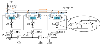
No spectral method addresses the full problem of hierarchical constraint generation in analog circuits with multiple symmetry lines. Moreover, prior approaches have only been applied to designs with a small number of blocks, with relatively simpler symmetries. To illustrate the complexity that must be addressed to solve the full problem, we consider the schematic of the FIR equalizer shown in Fig. 1, in which any mismatch between differential pair transistors {M1-M2},{M3-M4}, , {M19-M20} associated with the taps can result in a gain error. Moreover, the across current sources C0, , C9 should be the same to maintain similar overdrive current. A set of symmetry constraints, along multiple axes of symmetry, must be detected between the transistors in the differential pairs; the current sources must be self symmetric; each tap and its outputs must be symmetrically laid out with respect to resistors R1 and R2. The differential pairs also have symmetry requirements, and the current driver (shown in the inset for C9) requires ratioed structures with common-centroid layout for mismatch reduction.
A complicating factor is that the variable current sources, C0, , C9 may not be identical: in (Wong06, ), the first 4 taps use 7-bit current-steering DACs, while the rest employ 5-bit DACs. The bias voltage is the same for all taps: thus, despite the small difference in topology, the placement and routing must be matched. To the best of our knowledge, no existing technique addresses this problem of detecting symmetries between approximately identical analog blocks.
The requirements for a methodology that identifies symmetries in a netlist are: (1) Speed and scalability to large circuits; (2) Ability to identify constraints hierarchically; (3) Generality and applicability to a wide range of circuits; (4) Capability of identifying multiple axes of symmetry; (5) Capacity to identify symmetries between blocks that are approximately similar and need matching. Our work all requirements and has the following key features:
-
•
It hierarchically handles multiple symmetry levels using a graph-based framework, and identifies array structures.
-
•
It invokes a matching algorithm based on exact or approximate matching: the latter is based on finding graph edit distances, and employs a graph neural network (GNN) to detect matching in structures such as Fig. 1.
-
•
It demonstrates solutions on a range of design types, ranging from low-frequency analog to wireless designs.
Open-source software for this algorithm is available at (ALIGN-symmetry, ).
2. Our hierarchical approach
2.1. Graph representation and preprocessing
Inspired by (SubGemini, ), we represent a circuit netlist as an undirected bipartite graph . The set of vertices can be partitioned into two subsets, , corresponding to the elements (transistors/passives/ hierarchical blocks) in the netlist, and , the set of nets. For each element corresponding to vertex , if net is incident on , then the net vertex is connected to by an edge in . There are no edges between two elements in , or two nets in , and therefore the graph is bipartite. Edges to multiterminal elements are labeled to indicate which terminal connects to a net vertex, e.g., each edge from a transistor node is assigned a three-bit label () marking a gate, source, or drain connection. We traverse this graph to hierarchically identify structural symmetries.
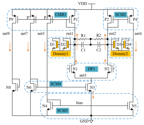
Initially, the graph is preprocessed using a traversal to identify the lowest level of building blocks, similar to library building blocks in (Eick10, ) or primitives in (gana, ). Primitives are composed from a few elements that form the basic building blocks of an analog circuit, and are specified by the user in a library. These are typically simple structures, e.g., passives or collections of a small number of transistors such as differential pairs, current mirrors, cascoded structures, or level shifters. For example, in the circuit in Fig. 2, four current mirrors – a current mirror bank (CMB1) and three single current mirrors (SCM2–SCM4), and a differential pair (DP) are mapped to library primitives. The elements in a primitive are collapsed into supernode vertices with labeled ports (net vertices) so that like ports of like vertices can be recognized for symmetry. For example, in a DP, the two transistor drain nodes are marked as symmetric and the source node is labeled so that it can be used in higher-level symmetry detection. Such primitive-level symmetry constraints are passed to the next level of hierarchy.
2.2. Symmetry detection algorithm
We propose a bottom-up approach that hierarchically detects symmetry constraints. At each level of hierarchy, symmetrical net information is passed to higher levels using ports whose information is used to identify matching at those levels.
After primitive blocks are identified using graph-based techniques (Eick10, ; gana, ) and primitive-level symmetries are identified, a search begins from all potentially symmetric pairs of node vertices , e.g., transistor drain nodes in a DP, or corresponding nodes of an SCM and CMB. For primitives CMB1 and SCM2 in Fig. 2, out1 could match with out2, and net4 could match with {net3, net7, net9}. Therefore, the candidate choices for are: (out1, out2), (net3, net4), (net7, net4) and (net9, net4). Similarly, DP1 leads to the candidate (out1,out2), also identified by CMB1/SCM2.
The overall algorithm for graph-based symmetry detection operates recursively and is described in Algorithm 1. It is initially invoked with set corresponding to all potential symmetry points from the primitive set. All vertices in the graph are marked as unexplored, except for supply and ground; the algorithm continues traversing the circuit graph and terminates when no unexplored node can be reached. The algorithm proceeds as follows:
Neighbor list For each pair of candidate points provided as an input to the algorithm, we invoke Neighbors(), which returns the unvisited neighbors of node (line 4). For transistors, these neighbors correspond to source/drain-connected vertices. For example, in Fig. 2, starting from the ports of DP1 (and so DP1 is marked as visited), for (out1, out2), the neighbor sets are {R1, C1, D1, D2, CMB1/out1} and {R2, C2, D3, D4, SCM2/out2}. (Note that for CMB1 and SCM2, we annotate the node vertices with the matching port.)
End case detection A recursive search is then carried out from the above list of neighbors, with the end case occurring when and have no unexplored neighbors, (line 5).
Finding groups of pairs
Next, MatchPair detects matches between the vertices of and , returning “group_of_pairs,” a set of all matching vertex pairs. For
example, in Fig. 2, starting from DP1, for
(out1, out2),
group_of_pairs = {(D1, D3), (D1, D4), (D2, D3), (D2, D4),
(R1, R2), (C1, C2), (CMB1/out1, SCM2/out2)}
Thus, from the cross-product of and , this list
eliminates pairs that do not match, e.g., (R1,C1). When FindSymmetricPairs
is recursively called, it traverses unvisited neighbors of these elements,
e.g., when (CMB1/out1, SCM2/out2), there are further recursive
calls to match (net3, net4), (net7, net4), and (net9, net4).
The MatchPair function can detect two types of matches:
An exact match, e.g., a two-terminal element such as a resistor,
represented by , matches a resistor of identical value, represented
by . For a multiterminal element such as transistors, edge labels
are also considered in pronouncing a match.
An approximate match, i.e., nonidentical structures to be
matched.
In Section 3, we show how a neural network is used to find
the graph edit distance (GED) to predict matches. If the GED is zero, the match
is exact, and if it is small, the match is approximate.
Processing matches Lines 9 – 18 consider the case where a single pair is detected. This means there is a single axis of symmetry for the pair. If and are identical, there is a self-symmetry that begins a new axis of symmetry. Otherwise we have a symmetric node pair that continues the previous axis; any matching constraints propagated from inside the block are added to .
For example, starting from CMB1 and SCM2, searching from corresponding ports (net3, net4), a unique pair (SCM3/out1, SCM3/out2) is found. Since these ports are symmetric, , and the new axis of symmetry lies at the center of SCM3. In the next recursive call, since the only unvisited neighbor of SCM3 is ground, the symmetric axis involving DP1, CMB1, SCM2, SCM3 is complete.
Lines 19 – 39 consider cases where more than one pair is matched: this may lead to axis of symmetry if multiple elements of the same type are matched, e.g., in Fig. 1. In lines 20 – 28, the exploration continues recursively from the matched pair until no further neighbors match. The valid matching paths, eliminating the nonconverging paths, are stored in valid_groups.
If valid_groups is a singleton, it is added to ; else, the multiple matches
correspond to an array of matching elements, rooted at and . Each
array is recognized as a hierarchical block, and the matched arrays are added
to . Array generation is performed by CreateArray()
(lines 33–34) by collecting a set of repeated
structures connected to a node of a graph . For the matches for (out1, out2) listed above, D1 and D2 each match with D3 and D4;
therefore, D1+D2 are grouped into array Dummy1, and D3+D4 into Dummy2. Matching
constraints are created between
(Dummy1, Dummy2), (R1, R2), (C1, C2)
(CMB1/out1, SCM2/out2)
A key contribution of this algorithm is its ability to build symmetry hierarchies, as shown in the case with (Dummy1, Dummy2) above. It could be argued that this simple illustrative case could be solved by defining a group of two dummy transistors as a primitive; however, the algorithm is general enough to handle more complex scenarios that other existing approaches cannot process. As an example, consider the FIR equalizer in Fig. 1 with multiple symmetries and array structures, as described in Section 1. If , the two nodes from the differential output, MatchPair would first detect the multiple matches corresponding to the DP. This would then be extended to a larger structure in valid_groups by also including the current source and XOR, where the current source is considered a match based on the approximate matching scheme to be described in Section 3. This combined structure, (DP + current source + XOR), is assembled into an array.
Finally, Line 41 discards if no match is found, and the search from terminates.
3. Error tolerant matching
3.1. Problem formulation
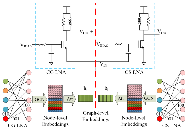
Fig. 1 had shown an example of the need for approximate matching, with a different numbers of bits being used in different taps of an equalizer: despite difference in the topology of the tap control bits, the circuit requires matching between taps for optimal performance. Fig. 3 illustrates another example that shows the matching requirement between a common-gate low-noise amplifier (CG-LNA) and a common-source LNA (CS-LNA) in a noise cancellation LNA. The two sides have a small difference in topology: the transistor source is connected to the capacitor terminal at left, but to ground at right.
These examples show that matching requirements are more complex than the simpler test cases typically handled in academic papers, and that matching is frequently required between parts that are similar but not identical. In fact, production analog designs use multiple techniques such as asymmetric dummy transistors in performance-critical parts (Lin12, ), noise cancellation circuits (Abidi05, ; Bruccoleri04, ), trim bits to handle noise and testing (Moreland, ; Carley89, ), and different device sizes for handling multiple bands in phased array systems (ehyaie2011, ).
This implies that the MatchPair function that detects symmetries must allow for minor changes in circuit topology. This is the inexact graph matching problem, and we map this to the Graph Edit Distance (GED) problem. The GED a measure of similarity between two graphs and : given a set of graph edit operations (insertion, deletion, vertex/edge relabeling), the GED is a metric of the number of edit operations required to translate to .
Let graphs and represent, respectively, the CS-LNA and the CG-LNA, as shown in Fig. 3, with element vertices at left and net vertices at right. To transform to , four edits are needed (i.e., GED = 4): (1) Deletion of two edges in : (capacitor element, ground net) and (transistor element (source label), net), and (2) Addition of two edges in : (capacitor element, net) and (transistor element (source label), ground net).
We calculate the similarity between two subblocks by comparing graph embedding of the two graphs. If the similarity is within a bound, the MatchPair function in Algorithm 1 returns a match.
3.2. Graph neural network formulation
The GED problem is NP-hard (Zeng09, ), implying that an exact solution is computationally expensive. This work uses a neural network that transforms the original NP-hard problem to a learning problem (bai18, ) for computing graph similarity.
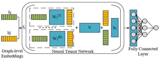
The method works in four steps: first, each node in the graph is converted to a node-level embedding vector; next, these embedding vectors are used to create a graph-level embedding of dimension . The lower half of Fig. 3 illustrates these two steps for the graphs for the CG-LNA and CS-LNA. For each subblock in the circuit, these steps need to be carried out once, and the graph embeddings are stored for matching any two pairs of subblocks in later stages. The computational complexity of these two steps is linear in the number of nodes in the graph. The last two steps are shown in Fig. 4. In the third step, the graph-level embeddings from the second step for two candidate graphs are fed to a trained neural tensor network that generates a similarity matrix between the graphs. The fourth step then processes this matrix using a fully connected neural network to yield a single score. This matching method for two subblocks uses the previously stored graph embeddings instead of the full subblock graphs. The complexity of these two steps is quadratic in , where is bounded by a small constant in practice, the procedure is computationally inexpensive as compared to an exact GED computational complexity which is exponential in the number of nodes of the graphs involved.
Node embedding stage: This stage transforms each node of a graph into a vector, encoding node features and neighborhood information in a manner that is representation-invariant. We use neighbor feature aggregation based on a three-layer graph convolutional network (GCN) (Kipf2017, ) to obtain the node embedding. The output in layer from the value in layer as:
| (1) |
where ReLU is the activation function, is the adjacency matrix of an undirected graph with added connections for each vertex to itself, is the diagonal matrix of , and are trainable weights for layer .
The GCN output, , is the node embedding matrix, . The row of , , is the embedding of node .
Graph embedding stage: For each graph to be compared, we now produce an embedding using the attention-based aggregation of node embeddings generated in the previous stage.
We first compute a global context, , for the graph, computed as weighted sum of node mbedding vector averages, followed by a nonlinear transformation, using trainable weights :
| (2) |
Here, is the number of nodes in the graph. Next, we use an attention mechanism to allow the model weights to focus on important parts of circuit, guided by the GED similarity metric. We empirically observe that nodes with high degree, and nodes forming special structures such as loops, get higher attention weights: this is because high-degree nodes receive contributions from a larger number of neighbors. The graph embedding is given by:
| (3) |
where is the sigmoid function.
Neural Tensor Network stage: Next, the relationship between two graph embeddings, , is measured using Neural Tensor Networks (NTNs) (reasoning2013, ) as:
| (4) |
where is a hyperparameter related to number of slices in the tensor, which controls the number of similarity scores produced by the model, is a weight tensor, is a weight vector, and is a bias vector.
Graph similarity score computation stage: The final step reduces the similarity scores in previous stage using a two-layer fully-connected neural network to provide a predicted similarity score . To train this network, the final score is compared against the ground truth GED score using the mean square error loss:
| (5) |
where is the set of training graph pairs.
3.3. Training and hyperparameter tuning
We have trained our network on 79 pairs of analog designs, where each pair has a small difference in topologies. Examples in our training set include single-ended vs. differential OTAs, multiple common-gate vs. common-source LNAs, OTAs with dummies, and arrays of current mirrors of different sizes. For each pair, the ground truth GED was computed using the algorithm in (zeina15, ), and a similarity metric between graphs and was defined as:
| (6) |
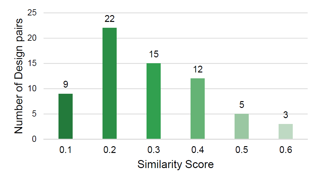
where () is the number of vertices (edges) in . The denominator normalizes the GED to the size of the graph. Next, recognizing that the GED score is more qualitative than quantitative (i.e., accuracy of multiple decimal places does not matter), we divide these distance scores into bins that define the level of similarity, as illustrated in Fig. 5. This score is used in Eq. (5) both for training and inference, to quantify the match between candidate pairs.
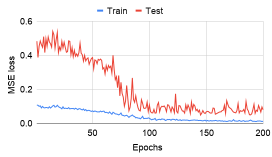
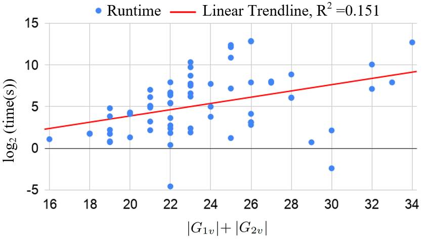
For a train:test ration of 51:28 among the 79 pairs, Fig. 7 shows the computation time for calculating correct GED: it can be seen to increase exponentially with the graph size.
We have experimented with several options in training with regard to the use of edge labels: recall that edge labels are used for vertices in the graph that represent multiterminal elements. The simplest version ignored the edge labels and performed matching without labels, while a more complex version required us to modify the graph embeddings at the GCN stage to enable the use of edge labels. We verified during training our model that the use of edge labels is important for improved accuracy as it provides more information about the presence of a drain/gate/source connection to a transistor.
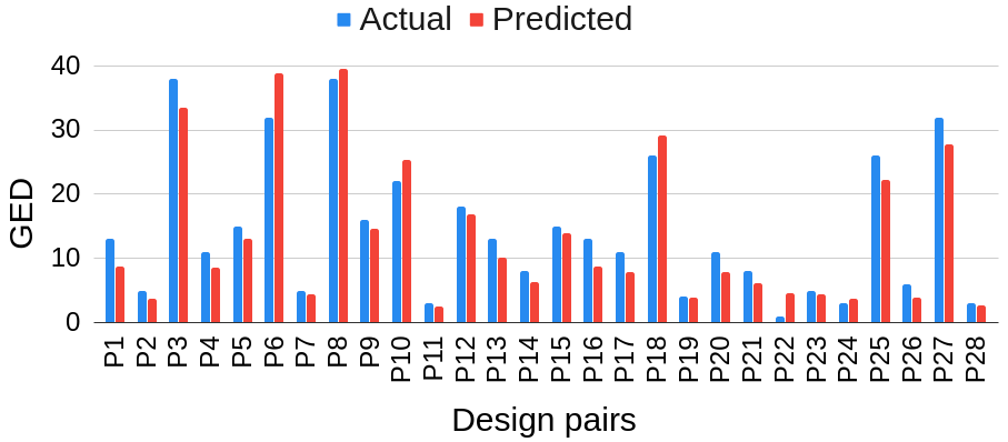
Fig. 7 illustrates the reduction of the loss metric in successive epochs during training. For both training and test phases, a steady reduction in loss is noted. Fig. 8 compares the GED predicted by our approach with the slower GED calculation from (zeina15, ), and shows a good match. The relatively small, but noticeable, magnitude of the difference is reflective of the fact that shows that many elements of the training set do not exercise a topology difference that involves a multiterminal element with labels.
Our optimized model is a three-layer GCN with 128 input channels (the number of channels is halved in each layer), with 8 slices in the NTN, and a fully connected network with one hidden layer after the NTN. The trained net uses .
4. Experimental results
We first present results on three designs that exercise hierarchical symmetries: the OTA of Fig. 2, an R-2R DAC shown in Fig. 9(top), and the FIR equalizer of Fig. 1. The characteristics of the graphs of these circuits are summarized in Table 1. These circuits contain sufficient complexity to exercise our method and demonstrate its validity and effectiveness. Our symmetry detection algorithm is integrated into the public-domain open-source analog layout tool, ALIGN (align, ), to generate layouts for these circuits. For clarity and to demonstrate the ability of our approach to identify symmetries, only the placement is shown, without routing.
| Method | #nodes | #Edges |
|---|---|---|
| OTA | 27 | 34 |
| R2R ladder | 116 | 144 |
| FIR equalizer | 640 | 1099 |
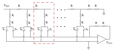
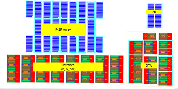
R-2R DAC (Fig. 9(top)): The main source of nonlinearity is mismatch between the array resistors. The area of the resistors in this circuit is significant as compared to the CMOS devices, and the resistors must be placed close to each other in a symmetric common-centroid configuration for matching. Our algorithm detects an array of the repeating R-2R module (shown using the dashed rectangle in the figure) and uses multiple instantiations of this to create an R-2R array. The OTA is also hierarchically recognized and extracted into a module. The switches and are part of a digital block, and may be placed outside the resistor array. The result of the ALIGN-generated layout using our constraint generation methodology is shown in Fig. 9(bottom).
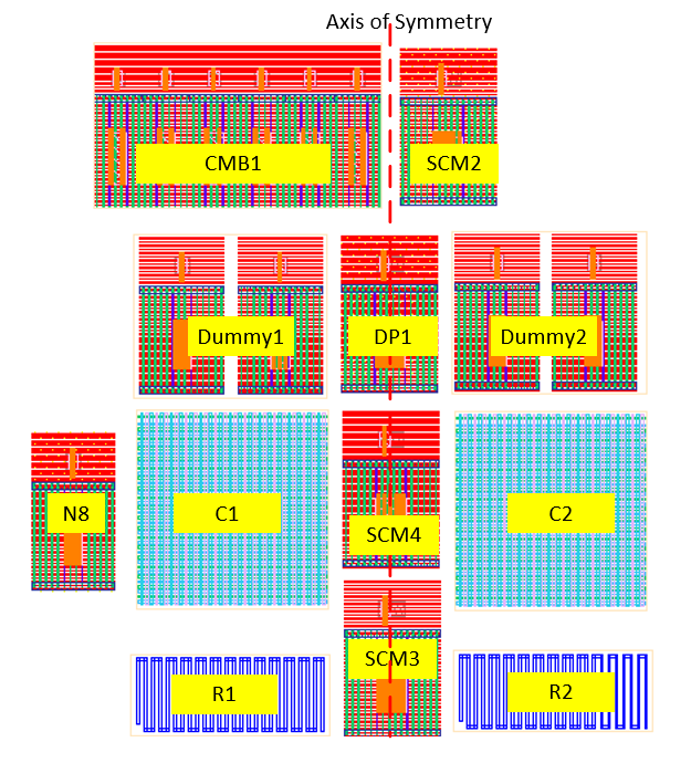
OTA circuit (Fig. 2): Our algorithm detects the symmetrical axis of the circuit, and the layout about the symmetric line is shown in Fig. 10. The dummy blocks, Dummy1 and Dummy2, that were detected (as described in Section 2.2) must be placed symmetrically with respect to the differential pair (DP1). Similarly, resistors R1 and R2 share the same symmetry axis with DP1, as do capacitors C1 and C2, the current mirrors SCM3 and SCM4. Transistors P1 and P2 are symmetric, and the transistors in CMB1 are in common-centroid.
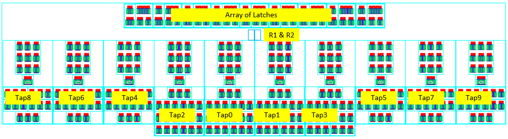
FIR Equalizer (Fig. 1): This circuit has ten taps for equalization, each containing an differential pair, a current mirror DAC, and CML XOR gate. All blocks in each tap share a common symmetry axis for matching. The first four taps use a 7-bit current mirror DAC, and the remaining taps have 5-bit current mirror DAC. To achieve better matching, the first four taps are placed in the center and the remaining taps are placed around these four, sharing a common symmetry axis. The layout of equalizer, shown in Fig. 11, meets all these requirements. This design demonstrates the detection and use of multiple lines of symmetry in a hierarchical way within primitives, within each tap, and globally at the block level.
The algorithm presented in this paper has been tested on a wide range of over a variety of circuits, including OTAs, buffers comparators, VCOs, analog-to-digital and digital-to-analog converters, and filters. The circuits are preprocessed to remove dummy transistors for which all terminals are connected to supply/ground lines.
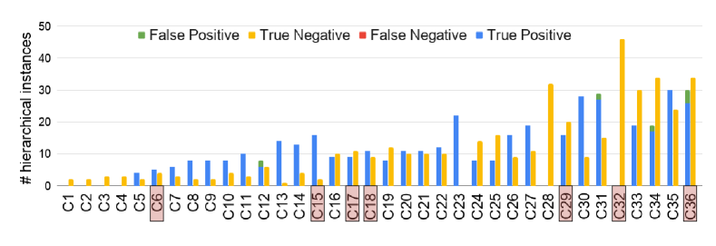
Beyond the three circuits discussed earlier, we were able to verify the correctness of the constraints through manual inspection on 36 circuits. The results of this verification, showing true/false positives and true/false negatives, are summarized in Fig. 12. For each hierarchical instance (e.g., device, passive, detected array) in the circuit, a true positive implies that the instance has a symmetry constraint that is correctly identified; a negative implies no symmetry constraint. Symmetrical instances must be connected using symmetrical nets. For the circuit names highlighted on the x-axis, our algorithm created a new hierarchy for arrays in these designs by grouping like elements. For the smallest circuits, it can be seen that no symmetries are identified. From C5 onwards, most circuits have some symmetry constraints (with the exception of C28, a DC-DC converter, and C32, an inverter-based VCO); a few circuits (C13, a fully differential telescopic OTA, and C23, a switched-capacitor filter) have symmetry constraints involving most/all devices. Most of the constraints detected by our algorithm are true positives or true negatives. No false negatives were detected.
Four circuits have false positives, related to (a) level-shifter structures connected to the output stages of amplifiers, and (b) dummy structures. The former is not harmful because it is connected symmetric current mirror units, and therefore it is logical to place these symmetrically even though matching is not required. The latter is a nonintuitive use of a dummy structure: since dummies are used for corrections subsequent to first silicon, it is recommended that any symmetries involving them should be annotated by the designer.
5. Conclusion
This paper has proposed an approach to handle multiple levels of symmetry hierarchies, including nested hierarchies, in analog circuits. The core algorithm is based on graph traversal through the network graph, and includes both exact graph-based matching and a novel machine learning based approximate matching technique using a GCN and a neural tensor network based GNN. We validate our results on a variety of designs, demonstrating the detection of multiple lines of symmetry, hierarchical symmetries, and common-centroid structure detection. We show how these guidelines are transferred for implementation to a layout generation tool that provides high layout quality.
Acknowledgements.
This work was supported in part by DARPA IDEA program under SPAWAR contract N660011824048.References
- (1) M. J. M. Pelgrom, et al., “Matching properties of MOS transistors,” IEEE J. Solid-St. Circ., vol. 24, no. 5, pp. 1433–1439, 1989.
- (2) R. Naiknaware and T. S. Fiez, “Automated hierarchical CMOS analog circuit stack generation with intramodule connectivity and matching considerations,” IEEE J. Solid-St. Circ., vol. 34, no. 3, pp. 304–317, 1999.
- (3) J. Scheible and J. Lienig, “Automation of analog IC layout: Challenges and solutions,” in Proc. ISPD, pp. 33–40, 2015.
- (4) K. Kunal, et al., “ALIGN: Open-source analog layout automation from the ground up,” in Proc. DAC, pp. 1–4, 2019.
- (5) E. Malavasi, et al., “Automation of IC layout with analog constraints,” IEEE T. Comput. Aid D., vol. 15, no. 8, pp. 923–942, 1996.
- (6) M. Eick, et al., “Automatic generation of hierarchical placement rules for analog integrated circuits,” in Proc. ISPD, pp. 47–54, 2010.
- (7) K. Kunal, et al., “GANA: Graph convolutional network based automated netlist annotation for analog circuits,” Proc. DATE, 2020.
- (8) M. Liu, et al., “S3DET: Detecting system symmetry constraints for analog circuits with graph similarity,” in Proc. ASP-DAC, pp. 193–198, 2020.
- (9) K.-L. J. Wong and C.-K. K. Yang, “A serial-link transceiver with transition equalization,” in Proc. ISSCC, pp. 223–232, 2006.
- (10) “ALIGN: Automatic circuit annotation.” https://github.com/ALIGN-analoglayout/hierarchical-symmetry.
- (11) M. Ohlrich, et al., “SubGemini: Identifying subcircuits using a fast subgraph algorithm,” in Proc. DAC, pp. 31–37, 1993.
- (12) C. Lin, et al., “Mismatch-aware common-centroid placement for arbitrary-ratio capacitor arrays considering dummy capacitors,” IEEE T. Comput. Aid D., vol. 31, no. 12, pp. 1789–1802, 2012.
- (13) S. Chehrazi, et al., “A 6.5 GHz wideband CMOS low noise amplifier for multi-band use,” in Proc. CICC, pp. 801–804, 2005.
- (14) F. Bruccoleri, et al., “Wide-band CMOS low-noise amplifier exploiting thermal noise canceling,” IEEE J. Solid-St. Circ., vol. 39, no. 2, pp. 275–282, 2004.
- (15) C. Moreland, et al., “A 14-bit 100-Msample/s subranging ADC,” IEEE J. Solid-St. Circ., vol. 35, no. 12, pp. 1791–1798, 2000.
- (16) L. R. Carley, “Trimming analog circuits using floating-gate analog MOS memory,” IEEE J. Solid-St. Circ., vol. 24, no. 6, pp. 1569–1575, 1989.
- (17) D. Ehyaie, Novel Approaches to the Design of Phased Array Antennas. PhD thesis, University of Michigan, Ann Arbor, MI, 2011.
- (18) Z. Zeng, et al., “Comparing stars: On approximating graph edit distance,” Proc. VLDB Endow., vol. 2, pp. 25–36, Aug. 2009.
- (19) Y. Bai, et al., “SimGNN: A neural network approach to fast graph similarity computation,” in Proc. WSDM, pp. 384–392, 2019.
- (20) T. Kipf, “Semi-supervised classification with graph convolutional networks,” in Proc. ICLR, 2017.
- (21) R. Socher, et al., “Reasoning with neural tensor networks for knowledge base completion,” in Proc. NeurIPS, pp. 926–934, 2013.
- (22) Z. Abu-Aisheh, et al., “An exact graph edit distance algorithm for solving pattern recognition problems,” in Proc. Int. Conf. Pattern Recognition Applications and Methods, pp. 271–278, 2015.