Nanoscale mechanics of antiferromagnetic domain walls
Abstract
Antiferromagnets offer remarkable promise for future spintronics devices, where antiferromagnetic order is exploited to encode information Jungwirth et al. (2018, 2016); Baltz et al. (2018). The control and understanding of antiferromagnetic domain walls (DWs) - the interfaces between domains with differing order parameter orientations - is a key ingredient for advancing such antiferromagnetic spintronics technologies. However, studies of the intrinsic mechanics of individual antiferromagnetic DWs remain elusive since they require sufficiently pure materials and suitable experimental approaches to address DWs on the nanoscale. Here we nucleate isolated, DWs in a single-crystal of Cr2O3, a prototypical collinear magnetoelectric antiferromagnet, and study their interaction with topographic features fabricated on the sample. We demonstrate DW manipulation through the resulting, engineered energy landscape and show that the observed interaction is governed by the DW’s elastic properties. Our results advance the understanding of DW mechanics in antiferromagnets and suggest a novel, topographically defined memory architecture based on antiferromagnetic DWs.
In the few years since its inception MacDonald and Tsoi (2011), the field of antiferromagnetic spintronics Jungwirth et al. (2018, 2016); Baltz et al. (2018) has seen significant progress, culminating in several demonstrations of antiferromagnet-based memory devices Marti et al. (2014); Wadley et al. (2016); Kosub et al. (2017). While the focus of these advances has been on directly controlling and reading the bulk Néel vector of antiferromagnets Song et al. (2018) and their domains Fiebig et al. (1995), the study and direct control of individual antiferromagnetic DWs has received much less attention thus far. Domain walls, however, are of particular relevance to the field, as they carry essential information on the magnetic microstructure of a material Hubert and Schäfer (1998); Weber et al. (2003), can have fundamentally different properties from the interior of domains Kummamuru and Soh (2008); Jaramillo et al. (2007), and delimit logical bits in magnetic memory devices Parkin et al. (2008). Furthermore, and akin to ferromagnet-based DW logic Allwood et al. (2005); Luo et al. (2020), the understanding and control of antiferromagnetic DWs could inform novel approaches to antiferromagnetic spintronics architectures.
In this work, we realise a key step towards harnessing antiferromagnetic DWs for spintronics applications and thereby gain valuable insights into DW physics in antiferromagnets. Specifically, we realise an instance of antiferromagnetic DWs whose morphologies are governed by DW elasticity and sample geometry – a key result we obtain by direct, real space imaging of antiferromagnetic DW trajectories with nanoscale resolution and over tens of micron lengthscales.
We demonstrate these results on the case of Cr2O3, a uniaxial, magnetoelectric antiferromagnet ordering at room temperature ( ) Brown (1969). Cr2O3’s magnetoelectric properties allow for a direct, local control of the Néel vector , through the combined application of electric and magnetic fields Brown (1969); Wadley et al. (2016). Additionally, symmetry breaking at the surface of Cr2O3 leads to a roughness-insensitive, uncompensated surface magnetic moment, that is directly linked to the underlying bulk Néel vector He et al. (2010); Belashchenko (2010), which can thereby be directly read out Kosub et al. (2015). These combined properties render Cr2O3 particularly interesting for antiferromagnetic spintronics Kosub et al. (2017); Jungwirth et al. (2016).
To address DW physics in Cr2O3, we employed nanoscale magnetic imaging using a single nitrogen vacancy (NV) electron spin in diamond as a scanning probe magnetometer Balasubramanian et al. (2008); Rondin et al. (2014). NV magnetometry is one of few nanoscale imaging methods for antiferromagnets Weber et al. (2003); Bode et al. (2006); Gross et al. (2017); Appel et al. (2019); Cheong et al. (2020), where it exploits stray magnetic fields resulting from uncompensated magnetic moments to address antiferromagnetic order. Such moments can generally result on surfaces Belashchenko (2010) or from spatial variations of the Néel vector Andreev and Marchenko (1980); Bode et al. (2006); Tveten et al. (2016) and are thereby particularly suitable for studying antiferromagnetic DWs. Here, we exploit Cr2O3’s surface magnetic moments He et al. (2010) for imaging.
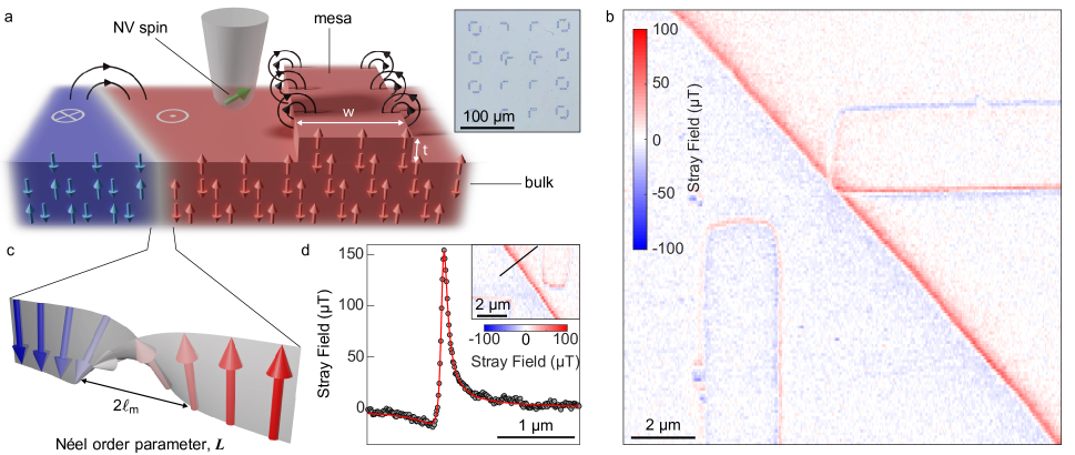
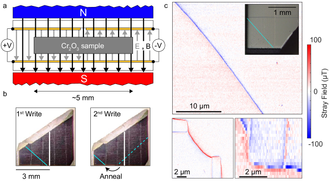
We performed our experiments on a oriented Cr2O3 single-crystal, -thick, with millimetre-scale lateral dimensions. To obtain position markers and a measurable magnetic stray field from the sample, even from uniformly ordered domains, we pattern a grid of micron-scale mesas (Fig. 1a, inset) with mean thickness and width on the sample surface using standard lithography (methods). To induce magnetic domains in the Cr2O3 sample, we employ magnetoelectric field cooling Brown (1969); Borisov et al. (2005) across . Specifically, we apply collinear electric and magnetic bias fields along the surface normal with mT and MV/m, where we used a split-gate capacitor to invert between two halves of the sample. We find this method of nucleation to be repeatable, reversible and necessary to observe DWs in the otherwise mono-domain sample (SI).
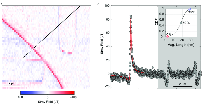
Figure 1b shows a representative NV magnetometry image of a section of the sample obtained at room temperature and in a weak bias magnetic field (mT) applied along the NV axis to achieve quantitative imaging Rondin et al. (2014). The data show stray magnetic fields emerging from a nucleated DW and from two mesas located on adjacent antiferromagnetic domains. From an analytical fit to the stray field across the mesa edges, we extract mean surface magnetizations (where the two signs apply to the different mesas), consistent with previous measurements Brown et al. (2002); Appel et al. (2019) and theoretical expectations Shi et al. (2009a). We confirm that these data are connected to the bulk antiferromagnetic order by performing temperature-dependant measurements, , where we observe that vanishes near Brown (1969). Details on the fitting routines and data for are given in the SI.
The DW we observe constitutes an interface between regions of oppositely aligned Néel vector, , through which rotates by over a characteristic lengthscale (Fig. 1c), where and are the exchange stiffness and magnetic anisotropy Hubert and Schäfer (1998). Using our measured value of as an input parameter, we perform an analytical fit to the magnetic stray field measured across the DW (Fig. 1d, inset) to determine a room temperature upper bound of nm, consistent with theoretical estimates (see SI). Strikingly, we find the DWs away from the mesas to be largely smooth and straight over length scales of tens of microns (see Fig. 1b and SI for further representative DW images), and do not observe a correlation between DW orientation and crystallographic directions of the sample.
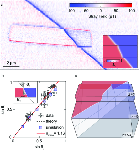
When a DW crosses a mesa, however, we observe considerable deviations from such straight DW paths, which bear similarity to the refraction of a light beam as described by Snell’s law in geometrical optics (Fig. 2a). Indeed, the crossing of the DW through the mesa incurs an energy cost, directly proportional to the increase in DW surface area resulting from the non-zero mesa height . The DW then assumes a path that minimizes its surface area (and thereby its surface energy), taking into account the local change in topography. To further support this picture, we mapped instances of such refraction-like behavior for a wide range of DW incidence angles, , as summarized in Fig. 2b. We determine by the DW direction off the mesa and define the outgoing angle from the DW direction at the center of the mesa (Fig. 2b, inset). Similar to Snell’s law, we find a linear behavior .
To obtain further insight into the observed DW mechanics, we perform spin lattice simulations SLa ; Pylypovskyi and Sheka (2013) that take into account nearest-neighbour antiferromagnetic exchange interactions, single-site anisotropy and the sample geometry (see Methods). We then obtain the equilibrium DW configuration through energy minimization of the spin lattice. The simulated DW profile on the sample surface (Fig 2a, inset) shows excellent agreement with the experimental data. Extracting from our simulations for varying values of confirms the experimentally observed linear relationship (Fig. 2b).
Our numerical results inspired an analytic ansatz for the DW profile, where we use a variational procedure to relate key parameters of the DW morphology to the mesa geometry (see SI). This analysis yields an analytic expression for (Fig. 2b, dashed line), where for small angles we find and additional terms . Although Snell’s law offers a useful analog to the observed phenomena, this result also highlights distinctions between the two. In particular, while the former arises from the principle of least action alone, the DW trajectory is additionally determined by the DW position in the bulk of the sample, far from the surface, which manifests in the existence of higher-order contributions of to .
Strikingly, the simulated DW trajectories also reproduce the marked bending of the DW towards the mesa edge normal, resulting in an ”S-shaped” distortion from the otherwise straight DW profile (Fig. 2a). This distortion arises from the minimization of the exchange interaction by normal incidence of DWs to surfaces (in this case, the mesa edge) Hubert and Schäfer (1998). This, together with the overall DW energy minimization, fully explains the observed DW trajectory on the mesa. Our simulation also yields the full, three dimensional morphology of the DW crossing the mesa (Fig. 2c), and shows how the mesa-induced distortion of the DW transitions towards the planar, bulk DW shape over a characteristic lengthscale . Through our analytic analysis, we find , which yields = .
The energy-penalty for traversing a mesa also leads to DW pinning phenomena at mesa edges. Specifically, we observe instances where the bulk DW position would intersect a mesa close to a corner, but is expelled from the mesa to minimise DW energy (Fig. 3a). This behavior is well reproduced in simulations, where we force the bulk DW to lie close to a mesa corner (Fig. 3a, inset). In such a case, the mesa presents a large DW energy barrier, and so the path, which minimises the overall energy, follows the mesa edge. The energetically favourable DW path (“refraction” or “pinning”) is therefore dependent on the mesa geometry and the location of the DW with respect to the mesa.
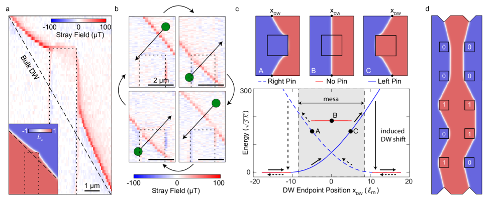
Importantly, we are able to de-pin the DW from a mesa corner and to place it on the mesa by using a focused laser spot to drag the DW (Fig. 3b). Such laser-dragging, previously demonstrated in the case of thin-film ferromagnets Tetienne et al. (2014), is based on laser-induced heating, which locally reduces the DW energy and therefore forms a movable potential well for the DW. We find that such local DW manipulation is facilitated by increasing the sample temperature, and therefore heat the sample to K. We then scan the laser at elevated powers, perpendicular to the DW and in absence of the scanning probe. As shown in Fig. 3b, we are able to reproducibly move the DW from lying on the mesa to a nearby location off the mesa and back, and thereby demonstrate the ability to achieve reliable and reversible DW manipulation.
We investigate this pinning and switching behavior more closely through simulations. In particular, we consider the energy of a DW whose end points we pin at fixed positions relative to a square mesa (Fig. 3c). By varying , we observe three distinct equilibrium DW configurations: a straight, undisturbed DW, or the DW pinned to either side of the mesa. The energy and snapshots of these configurations are shown as a function of in Fig. 3c. In the case of a straight DW, the DW energy increases abruptly upon crossing the mesa, where the energy-step can be tuned by the mesa height. For the pinned DWs, the DW area, and hence the DW energy, increases gradually with increasing DW deflection. In particular, this observed pinning behavior shows that the DW mimics an elastic surface, which can be deformed. The mechanical surface tension of the DW (energy per unit area) can be determined by the material properties and determines the energy excess resulting from the interaction between the DW and mesa (see SI). For sufficiently strong deflections, the energy of the pinned state exceeds that of a straight DW, leading to a metastable configuration. When this happens, applying a stimulus (e.g. magnetoelectric pressure or local heating) can cause a sudden change in the DW state (vertical arrows in Fig. 3c). This switching process is hysteretic and controllable by the mesa-height and the strength of the stimulus.
These combined results suggest a novel architecture for a scalable, DW-based antiferromagnetic memory as outlined in Fig. 3d. Specifically, we propose to employ nanoscale mesas as engineered DW pinning centers, where binary information is encoded by the direction of on a given mesa. By fabricating sufficiently thick mesas, one can energetically exclude the case of an unpinned DW, thereby creating a bistable system where the DW is forced to pin to one edge of the mesa or the other. The size of the resulting antiferromagnetic memory bits is then limited by only, opening the route to bits of nanoscale dimension – a significant improvement on currently demonstrated architectures for antiferromagnetic memories Wadley et al. (2016); Kosub et al. (2017). We demonstrated the possibility to switch and read such bits by laser dragging and magnetometry, but integrated, all-electrical approaches could be readily envisaged. In particular, electrical gates on the mesas could be used to apply magnetoelectric pressure He et al. (2010); Ashida et al. (2015) for switching, and to exploit the anomalous Hall effect Kosub et al. (2015) for all-electrical readout.
In conclusion, we demonstrated the deterministic generation and control of pristine DWs in a single-crystal antiferromagnet, and observed DW physics determined solely by sample geometry and the DW surface energy, while defect-related DW pinning mechanisms Lemerle et al. (1998) appear negligible. These combined achievements, together with the versatile toolset of quantum sensing Degen et al. (2017), offer attractive avenues to exploring largely uncharted areas of DW physics, such as DW creep Chauve et al. (2000); Ferré et al. (2013) or DW magnons in antiferromagnets Flebus et al. (2018). Based on the generality and robustness of our modeling (see Methods), we conclude that our results should be extendable to other achiral, uniaxial antiferromagnets and open multiple avenues for future research of fundamental and applied nature, be it in the form of the proposed antiferromagnetic memory devices, or ultimately for the realisation of DW logic Allwood et al. (2005). Through simulations, we expect the same behavior seen here in bulk, to manifest in high-quality, thin-film samples – a key materials frontier that remains to be addressed in future work.
I Methods
I.1 Sample Preparation
The Cr2O3 used in this study is a commercially available, single crystal from MaTeK with a (0001) surface orientation. The originally crystal was broken into two halves along a diagonal (see SI). The sample was prepared by removing magnetic contamination (presumably resulting from the polishing process) with a ArCl2 plasma etch (ICP-RIE, Sentech) in steps. One side of the crystal was then spin coated with an HSQ layer (FOx, Dow Corning) and subsequently developed using electron-beam lithography to create mesa masks. These mask patterns were transferred into the sample with a ArCl2 plasma etch. The masks were then removed using HF. This process results in the -tall structures seen in the inset of Fig. 1a. For the measurements, the sample was mounted on a small Peltier element, placed on top of an open-loop, piezoelectric scanner (Attocube ANSxyz100), allowing us to heat the sample up to .
I.2 NV Magnetometry
The NV center is a point defect in diamond, whose S=1 electronic ground state spin can be initialized and read-out through optical excitation at . Specifically, we use state-dependent fluorescence to identify the Zeeman splitting between the spin levels using optically detected magnetic resonance (ODMR). All measurements in this study were performed using scanning, all-diamond parabolic pillars Hedrich et al. (2020) housing a single NV center and integrated into a custom confocal imaging setup equipped with a CW laser Grinolds et al. (2013). The measurements were performed with of continuous-wave optical excitation, a factor of two smaller than typical saturation powers for NVs in these parabolic scanning pillars Hedrich et al. (2020). The microwave (MW) needed to manipulate the NV is provided by a gold loop antenna with a typical effective driving strength of at the NV. These low excitation powers (both MW and laser) ensure that we do not disturb the DW, which was confirmed by repeating scans and observing the DW. A small bias magnetic field () was applied along the NV axis using a permanent magnet to allow for a sign-sensitive measurement of the stray magnetic fields.
Both 2D magnetic field images and linescans were performed using a feedback technique to lock a microwave driving frequency to the instantaneous NV spin transition frequency, as described in Schoenfeld and Harneit (2011). We employ single-pixel integration times ranging from for full-field images to for individual line scans with a noise floor of .
I.3 Domain Wall Nucleation
DWs are nucleated in the otherwise mono-domain single crystal Cr2O3 using magnetoelectric cooling through the Néel temperature. A uniform magnetic field is achieved by placing two permanent magnets adjacent to each other and in close proximity to the sample. The result is a nearly homogeneous magnetic field of mT along the center normal, as measured by a Hall probe (AS NTM, FM302 Teslameter, Projekt Elektronik). In addition, we apply electric fields across the sample using a split-gate capacitor consisting of two quartz plates with Au evaporated onto the surface. The Cr2O3 sample is then centered onto the capacitor gap and sandwiched between the top and bottom gate together with thin mica sheets to prevent electroplating of Au onto the crystal surface. A schematic of this setup may be found in the SI. The whole device is then heated to far above the Néel temperature and allowed to cool to room temperature while simultaneously applying between the electrodes leading to an electric field of across the crystal. The resulting VT/m is sufficient to force the Cr2O3 sample into a two-domain state. The crystal can again be made mono-domain by repeating this procedure with a uniform capacitor rather than the split-gate. This process has been repeated twice to show the reproducibility, where each realization resulted in a different domain configuration (see SI).
I.4 Domain Wall Dragging
The repeated movement of the DW is demonstrated via local heating with a laser - a process we describe as ”laser dragging”. For this, we remove the NV scanning probe and focus the laser onto the sample surface with a beam diameter of . We scan the sample at a speed of roughly , perpendicular to the DW, over distances exceeding before reducing the laser power back to below . With this method, the minimum laser power at which we have observed DW motion is . We then replace the NV scanning probe and image the new DW position. These experiments were performed at a sample temperature of K, achieved through heating with the Peltier element. This domain wall dragging can also be verified through direct measurements with the NV (see SI).
I.5 Fitting to Mesa Stray Fields
The mesa structures etched into the surface of Cr2O3 play a critical role in our study as they act as sources of stray fields for characterizing the surface magnetization () and NV-sample spacing () as well as providing reference markers. For the former, we consider 29 linecut sections, each taken over a mesa, and fit the stray field at the mesa edges by modifying a well-studied model Tetienne et al. (2015), which describes the stray field as arising from line currents along the top and bottom edges of the mesa (see SI). We obtain estimates of the NV angles ( and ), , and the mesa edge positions, as well as their variances, through the Metropolis Hastings (MH) algorithm (see SI). In particular, by multiplying the likelihood distributions of all 29 datasets, performed at various temperatures, we obtain reasonable estimates of the NV angles, and degrees. We furthermore extract a mean nm. By considering only the six measurements taken at room temperature, we determine the value for the surface moment density, /nm2, where the error corresponds to the standard deviation of the measurements.
I.6 Fitting to Domain Wall Stray Fields
To describe the stray field of a domain wall in Cr2O3, we begin with the typical description of the evolution of the magnetic moments of the two sublattices in this collinear antiferromagnet Belashchenko et al. (2016); Mitsumata and Sakuma (2011). For this, we assume a Bloch wall of the typical form:
| (1) | ||||
| (2) | ||||
| (3) |
where is the magnetic length, as given in the main text. Thus, the domain wall profile (as shown in Fig. 1c) is determined by , allowing us to use this parameter to characterize the domain wall width. This form of the domain wall profile is then considered in the derivation of the stray field along the NV axis, as described in the SI.
We again use the MH algorithm to evaluate our model of the stray field with the stray field data. To do so, the NV-sample spacing, angles and surface magnetization previously extracted from the mesa fits are used as prior information in the fit. In particular, we consider the NV-sample spacing on a case-by-case basis as each DW linescan is taken concurrently with a mesa linescan. The upper bound for stated in the main text is then obtained from the extracted likelihood distributions at room temperature. We examine the extrema of the distributions, selecting the 98th percentile of the cumulative distribution function (CDF) as the upper limit on . This implies that, at room temperature, our data excludes an larger than .
We note that for completeness, the strayfield data has also been analyzed under the assumption of a Néel wall, resulting in a similar quality fit for slightly changed model parameters. However, the resulting domain wall width is consistently smaller for a Néel wall, verifying the validity of our statement on the upper limit of , regardless of wall type.
I.7 Simulation Details
The spin-lattice simulations are performed in the in-house developed SLaSi package SLa ; Pylypovskyi and Sheka (2013), rewritten in the CUDA framework, and based on a generic antiferromagnet consisting of a simple cubic lattice, described by the effective Hamiltonian:
| (4) | ||||
Here, is the exchange integral, is the easy-axis () anisotropy, is the unit vector representing the direction of the magnetic moment at the -th lattice site and runs over the nearest neighbors of , yielding the oppositely oriented magnetic sublattices. To represent a general antiferromagnet, all while approximating the properties of Cr2O3, we set , nm, = 2.34pJ Shi et al. (2009a) and = pJ, which leads to . These values allow for a reasonable scale of the sample for spin-lattice simulations and properly reproduce the effects observed in experiments. The last term in Hamiltonian (4) represents the dipolar interaction, which we control by the parameter . We find that dipolar interactions do not change the results of our simulations qualitatively nor quantitatively, and therefore favor in the following, consistent with other studies.
With this, we solve the set of Landau-Lifshitz-Gilbert equations
| (5) |
where is the Gilbert damping, using the Runge-Kutta-Fehlberg scheme of order 4-5 with a fixed time step to find the equilibrium magnetic state when . We simulate parallelepiped-shaped samples with the mesa faces coinciding with lattice planes. This is done without loss of generality, as simulations with arbitrarily oriented mesas show no significant variations.
To simulate a given bulk domain wall position, in particular for the study shown in Fig. 3c, we fix the equilibrium domain wall by notches at the sample boundaries. The initial state is defined as either a straight DW, which can cross the mesa, or one which is pinned at and bent around the mesa edges. The magnetization is then relaxed and its energy is compared to that of an unperturbed domain wall far from the mesa. The excess energy of the initial state can cause the DW to switch from a high energy (strongly extended) to low energy state, thereby imitating an induced switch due to an external stimulus. We note that the present model contains no bias to select a particular DW type (Bloch, Néel, or other). The resulting equilibrium DW type in the simulations is thus determined by the initial magnetic state we choose before numerical relaxation and may also vary along the DW. We varied details of the initial conditions and observed no influence of the DW type on the relaxed DW trajectory.
Finally, to further investigate the robustness of our model, we performed simulations where we lower the structural symmetry of the lattice by shifting the two magnetic sublattices we consider by half a lattice constant with respect to each other along the main axis of the cubic lattice. Here, we also observe quantitatively similar results as for the original, simple cubic lattice, indicating that our model is indeed robust against variations in model parameters. Thus, though the considered spin-lattice is not a perfect representation of the Cr2O3 spin-lattice, these simplifications appear justified as our minimal model already captures all features of DW mechanics observed in our experiments. Furthermore, the generality of this model means it should be applicable to any achiral, uniaxial antiferromagnet.
II Acknowledgements
We thank O. Gomonay and S.A. Díaz for fruitful discussions and M. Fiebig and M. Giraldo for optical characterisation of our Cr2O3 samples at an early stage of the experiment. We would further like to thank M. Kasperczyk and P. Amrein for their help with efficient implementations of the Metropolis-Hastings algorithm, A. Kákay at the HZDR for providing us with computation time for micromagnetics, and D. Broadway and L. Thiel for valuable input on figures. We would also like to thank A.V. Tomilo at the TSNUK for his help with the spin-lattice simulations as well as his very helpful insight.
We gratefully acknowledge financial support through the NCCR QSIT, a competence centre funded by the Swiss NSF, through the Swiss Nanoscience Institute, by the EU FET-OPEN Flagship Project ASTERIQS (grant ), SNF Project Grant , German Research Foundation (projects MA and MA ) and Taras Shevchenko National University of Kyiv (Project No. BF).
References
- Jungwirth et al. (2018) T. Jungwirth, J. Sinova, A. Manchon, X. Marti, J. Wunderlich, and C. Felser, Nature Physics 14, 200 (2018).
- Jungwirth et al. (2016) T. Jungwirth, X. Marti, P. Wadley, and J. Wunderlich, Nat. Nano. 11, 231 (2016).
- Baltz et al. (2018) V. Baltz, A. Manchon, M. Tsoi, T. Moriyama, T. Ono, and Y. Tserkovnyak, Rev. Mod. Phys. 90, 015005 (2018).
- MacDonald and Tsoi (2011) A. H. MacDonald and M. Tsoi, Philosophical Transactions of the Royal Society A: Mathematical, Physical and Engineering Sciences 369, 3098 (2011).
- Marti et al. (2014) X. Marti, I. Fina, C. Frontera, J. Liu, P. Wadley, Q. He, R. J. Paull, J. D. Clarkson, J. Kudrnovský, I. Turek, J. Kuneš, D. Yi, J.-H. Chu, C. T. Nelson, L. You, E. Arenholz, S. Salahuddin, J. Fontcuberta, T. Jungwirth, and R. Ramesh, Nature Materials 13, 367 (2014).
- Wadley et al. (2016) P. Wadley, B. Howells, J. Železnỳ, C. Andrews, V. Hills, R. P. Campion, V. Novak, K. Olejník, F. Maccherozzi, S. Dhesi, et al., Science 351, 587 (2016).
- Kosub et al. (2017) T. Kosub, M. Kopte, R. Hühne, P. Appel, B. Shields, P. Maletinsky, R. Hübner, M. O. Liedke, J. Fassbender, O. G. Schmidt, and D. Makarov, Nature Communications 8, 13985 (2017).
- Song et al. (2018) C. Song, Y. You, X. Chen, X. Zhou, Y. Wang, and F. Pan, Nanotechnology 29, 112001 (2018).
- Fiebig et al. (1995) M. Fiebig, D. Fröhlich, G. Sluyterman v. L., and R. V. Pisarev, Applied Physics Letters 66, 2906 (1995).
- Hubert and Schäfer (1998) A. Hubert and R. Schäfer, “Magnetic domains: The analysis of magnetic microstructures,” (Springer, 1998) Chap. 3.2.7(D).
- Weber et al. (2003) N. B. Weber, H. Ohldag, H. Gomonaj, and F. U. Hillebrecht, Phys. Rev. Lett. 91, 237205 (2003).
- Kummamuru and Soh (2008) R. K. Kummamuru and Y.-A. Soh, Nature 452, 859 (2008).
- Jaramillo et al. (2007) R. Jaramillo, T. F. Rosenbaum, E. D. Isaacs, O. G. Shpyrko, P. G. Evans, G. Aeppli, and Z. Cai, Phys. Rev. Lett. 98, 117206 (2007).
- Parkin et al. (2008) S. Parkin, M. Hayashi, and L. Thomas, Science 320, 190 (2008).
- Allwood et al. (2005) D. A. Allwood, G. Xiong, C. Faulkner, D. Atkinson, D. Petit, and R. Cowburn, Science 309, 1688 (2005).
- Luo et al. (2020) Z. Luo, A. Hrabec, T. P. Dao, G. Sala, S. Finizio, J. Feng, S. Mayr, J. Raabe, P. Gambardella, and L. J. Heyderman, Nature 579, 214 (2020).
- Brown (1969) C. Brown, Magnetoelectric Domains in Single Crystal Chromium Oxide, Ph.D. thesis, Imperial College (1969).
- He et al. (2010) X. He, Y. Wang, N. Wu, A. N. Caruso, E. Vescovo, K. D. Belashchenko, P. A. Dowben, and C. Binek, Nature Materials 9, 579 (2010).
- Belashchenko (2010) K. D. Belashchenko, Phys. Rev. Lett. 105, 147204 (2010).
- Kosub et al. (2015) T. Kosub, M. Kopte, F. Radu, O. G. Schmidt, and D. Makarov, Phys. Rev. Lett. 115, 097201 (2015).
- Balasubramanian et al. (2008) G. Balasubramanian, I. Chan, R. Kolesov, M. Al-Hmoud, J. Tisler, C. Shin, C. Kim, A. Wojcik, A. Hemmer, P.R. amd Krueger, T. Hanke, A. Leitenstorfer, R. Bratschitsch, F. Jelezko, and J. Wrachtrup, Nature 455, 648 (2008).
- Rondin et al. (2014) L. Rondin, J.-P. Tetienne, T. Hingant, J.-F. Roch, P. Maletinsky, and V. Jacques, Reports on Progress in Physics 77, 56503 (2014).
- Bode et al. (2006) M. Bode, E. Y. Vedmedenko, K. von Bergmann, A. Kubetzka, P. Ferriani, S. Heinze, and R. Wiesendanger, Nature Materials 5, 477 (2006).
- Gross et al. (2017) I. Gross, W. Akhtar, V. Garcia, L. J. Martínez, S. Chouaieb, K. Garcia, C. Carrétéro, A. Barthélémy, P. Appel, P. Maletinsky, J. V. Kim, J. Y. Chauleau, N. Jaouen, M. Viret, M. Bibes, S. Fusil, and V. Jacques, Nature 549, 252 (2017).
- Appel et al. (2019) P. Appel, B. J. Shields, T. Kosub, N. Hedrich, R. Hübner, J. Fassbender, D. Makarov, and P. Maletinsky, Nano Letters 19, 1682 (2019).
- Cheong et al. (2020) S.-W. Cheong, M. Fiebig, W. Wu, L. Chapon, and V. Kiryukhin, npj Quantum Materials 5, 1 (2020).
- Andreev and Marchenko (1980) A. F. Andreev and V. I. Marchenko, Soviet Physics Uspekhi 23, 21 (1980).
- Tveten et al. (2016) E. G. Tveten, T. Müller, J. Linder, and A. Brataas, Phys. Rev. B 93, 104408 (2016).
- Borisov et al. (2005) P. Borisov, A. Hochstrat, X. Chen, W. Kleemann, and C. Binek, Phys. Rev. Lett. 94, 117203 (2005).
- Brown et al. (2002) P. J. Brown, J. B. Forsyth, E. Lelièvre-Berna, and F. Tasset, J. Phys.: Condens. Matter 14, 1957 (2002).
- Shi et al. (2009a) S. Shi, A. L. Wysocki, and K. D. Belashchenko, Physical Review B 79, 104404 (2009a).
- (32) “SLaSi spin–lattice simulations package,” http://slasi.knu.ua, accessed: 2019-07-12.
- Pylypovskyi and Sheka (2013) O. V. Pylypovskyi and D. D. Sheka, in Book of Abstract of 11th EUROPT Workshop on Advances in Continuous Optimization, Florence, Italy, June 26-28, 2013 (Florence, 2013) p. 11.
- Tetienne et al. (2014) J.-P. Tetienne, T. Hingant, J.-V. Kim, L. H. Diez, J.-P. Adam, K. Garcia, J.-F. Roch, S. Rohart, A. Thiaville, D. Ravelosona, and V. Jacques, Science 344, 1366 (2014).
- Ashida et al. (2015) T. Ashida, M. Oida, N. Shimomura, T. Nozaki, T. Shibata, and M. Sahashi, Applied Physics Letters 106, 132407 (2015).
- Lemerle et al. (1998) S. Lemerle, J. Ferré, C. Chappert, V. Mathet, T. Giamarchi, and P. Le Doussal, Phys. Rev. Lett. 80, 849 (1998).
- Degen et al. (2017) C. L. Degen, F. Reinhard, and P. Cappellaro, Reviews of Modern Physics 89, 035002 (2017).
- Chauve et al. (2000) P. Chauve, T. Giamarchi, and P. Le Doussal, Phys. Rev. B 62, 6241 (2000).
- Ferré et al. (2013) J. Ferré, P. J. Metaxas, A. Mougin, J.-P. Jamet, J. Gorchon, and V. Jeudy, Comptes Rendus Physique 14, 651 (2013).
- Flebus et al. (2018) B. Flebus, H. Ochoa, P. Upadhyaya, and Y. Tserkovnyak, Phys. Rev. B 98, 180409 (2018).
- Hedrich et al. (2020) N. Hedrich, D. Rohner, M. Batzer, P. Maletinsky, and B. J. Shields, arXiv:2003.01733 (2020).
- Grinolds et al. (2013) M. S. Grinolds, S. Hong, P. Maletinsky, L. Luan, M. D. Lukin, R. L. Walsworth, and A. Yacoby, Nature Physics 9, 215 (2013).
- Schoenfeld and Harneit (2011) R. Schoenfeld and W. Harneit, Physical Review Letters 106, 030802 (2011).
- Tetienne et al. (2015) J.-P. Tetienne, T. Hingant, L. Martinez, S. Rohart, A. Thiaville, L. H. Diez, K. Garcia, J.-P. Adam, J.-V. Kim, J.-F. Roch, and et al., Nature Communications 6, 6733 (2015).
- Belashchenko et al. (2016) K. D. Belashchenko, O. Tchernyshyov, A. A. Kovalev, and O. A. Tretiakov, Applied Physics Letters 108, 132403 (2016).
- Mitsumata and Sakuma (2011) C. Mitsumata and A. Sakuma, IEEE Transactions on Magnetics 47, 3501 (2011).
- Robert (2015) C. P. Robert, The Metropolis-Hastings Algorithm (Wiley Stats Ref: Statistics Reference Online, 2015) pp. 1–15.
- Bolstad (2009) W. Bolstad, Bayesian Statistics Using Conjugate Priors (Wiley Online Library: Understanding Computational Bayesian Statistics, 2009) pp. 61–100.
- Rohner et al. (2019) D. Rohner, J. Happacher, P. Reiser, M. A. Tschudin, A. Tallaire, J. Achard, B. J. Shields, and P. Maletinsky, Applied Physics Letters 115, 192401 (2019).
- Dovzhenko et al. (2018) Y. Dovzhenko, F. Casola, S. Schlotter, T. X. Zhou, F. Büttner, R. L. Walsworth, G. S. D. Beach, and A. Yacoby, Nature Communications 9, 2712 (2018).
- Vansteenkiste et al. (2014) A. Vansteenkiste, J. Leliaert, M. Dvornik, M. Helsen, F. Garcia-Sanchez, and B. V. Waeyenberge, AIP Advances 4, 113007 (2014).
- Kota et al. (2013) Y. Kota, H. Imamura, and M. Sasaki, Applied Physics Express 6, 013002 (2013).
- Mu et al. (2013) S. Mu, A. L. Wysocki, and K. D. Belashchenko, Physical Review B 87, 054435 (2013).
- Al-Mahdawi et al. (2017) M. Al-Mahdawi, Y. Shiokawa, S. P. Pati, S. Ye, T. Nozaki, and M. Sahashi, Journal of Physics D: Applied Physics 50, 155004 (2017).
- Foner (1963) S. Foner, Phys. Rev. 130, 183 (1963).
- Hoser and Koebler (2012) A. Hoser and U. Koebler, Renormalization Group Theory (Springer Berlin Heidelberg, 2012).
- Parthasarathy and Rakheja (2019) A. Parthasarathy and S. Rakheja, Phys. Rev. Applied 11, 034051 (2019).
- Shi et al. (2009b) S. Shi, A. L. Wysocki, and K. D. Belashchenko, Physical Review B 79, 104404 (2009b).
- Samuelsen et al. (1970) E. Samuelsen, M. Hutchings, and G. Shirane, Physica 48, 13 (1970).
- Mu and Belashchenko (2019) S. Mu and K. D. Belashchenko, Physical Review Materials 3, 034405 (2019).
- Auerbach (1994) A. Auerbach, Interacting Electrons and Quantum Magnetism (Springer New York, 1994).
- Ivanov (2005) B. A. Ivanov, Low Temperature Physics 31, 635 (2005).
- Dudko et al. (1971) K. L. Dudko, V. V. Eremenko, and L. M. Semenenko, Physica Status Solidi (b) 43, 471 (1971).
- Gomonay and Loktev (2007) H. V. Gomonay and V. M. Loktev, Physical Review B 75, 174439 (2007).
- Kota and Imamura (2016) Y. Kota and H. Imamura, Applied Physics Express 10, 013002 (2016).
Supplementary Information
III Position Calibration and Error Analysis
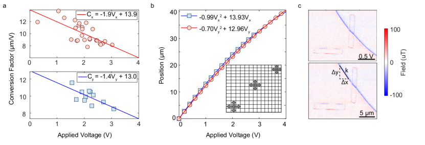
As we are using open-loop piezo scanners (Attocube ANSxyz100), we need to calibrate their physical displacement and determine the piezo non-linearity in order to achieve accurate fitting of the domain wall. To do so, we perform atomic force microscopy (AFM) measurements of our sample’s topography on a commercial system (Bruker Dimension 3100), and compare various length scales as offered by patterned mesas on the sample surface to those measured by our system. This allows us to determine the conversion factor from applied voltage (V) to physical piezo displacement () for a wide range of piezo voltages as shown in Fig. 4a. Errors on individual points here are below the marker size. We integrate the fitting functions given in the legends to convert from our system coordinates (in voltage) to real coordinates (in ) as shown in Fig. 4b. This leads a non-linear conversion, which corrects for deformations in our measurements (Fig. 4b, inset). We make this explicit by showing a 2D stray field image in Fig. 4c, where the original image (with scale in applied voltage) is shown in the top panel and the adjusted scaling conversion in the bottom panel. The difference between the two images is most apparent when one compares the visible curvature of the domain wall in both figures.
From these conversion factors, we can also obtain an estimate of the uncertainty in our displacement calibration. We compare the mesa dimensions measured in our setup to those measured with the Bruker Dimension 3100 AFM and obtain a 10% error. We therefore assume a 10% uncertainty on quantities such as the and that factor into the error bars in Fig. 2b in the main text. This uncertainty will also appear in the mesa width used to determine the magnetization and the NV-to-sample separation.
Finally, let us further examine the error analysis for the domain wall (DW) deflection angles. Assuming , we obtain , where is the slope of the domain wall in the bulk (on the mesa) (see Fig. 4c), which can then be converted to an error on through simple error propagation. This results in
| (6) |
which is plotted as the error bars in Fig. 2b of the main text. We then use a linear regression, to obtain the final estimate of . The remaining error analysis will be addressed in later sections.
IV Domain Wall Nucleation and Morphology
As received, the single crystal Cr2O3 was in a mono-domain state, confirmed with high probability by measuring the same sign of the surface magnetization at number of mesas (see Section VI) across the surface of the crystal. The DW is then nucleated as described in the methods and using the device shown in Fig. 5a. We use the same method of sampling the magnetization across the sample to localize the DW. The nucleated DWs appear smooth and straight, as seen when imaging the domain wall over larger areas. The approximate orientation of the DW, as determined by NV magnetometry, is shown in Fig. 5b with cyan lines for subsequent nucleation procedures, separated by an erasure of the domain wall through electromagnetic cooling in a homogeneous field. Note that these positions differ from the nominal location of the split-gate gap (shown by a thick, white line), indicating that the domain wall is mobile during the nucleation process. Furthermore, upon annealing the sample at , the domain wall position changed drastically, as shown in the right panel of Fig. 5b, where the initially nucleated position is shown with a dashed line, and the final position, after annealing is shown with a solid line. We would like to note that the observation that a domain wall may persist even when heated above the Néel temperature is not a new one, and that this phenomenon was already explored by Brown in 1969 Brown (1969). We also show an additional stray field image of the domain wall in Fig. 5c, taken at the bottom right of the cyan line shown in the inset. This emphasizes the fact that the domain wall, in the absence of mesa structures and strong pinning centers, is indeed smooth at the micrometer scale and suggests that the pinning we observe is primarily due to the interaction between mesa and DW. Further examples of this pinning are shown in the bottom two panels of Fig. 5c. In these two images, we observe simultaneous pinning at multiple mesa edges following both nucleated instances of the domain wall.
V Metropolis Hastings
We use a form of the Metropolis Hastings (MH) algorithm to infer the probability distributions of parameters in difficult-to-sample data sets Robert (2015); Bolstad (2009). This MH-based parameter estimation is chosen, since the model involves correlated parameters and exhibits many local good fits to the data. Such conditions make it difficult for gradient descent methods to determine a global minimum in the difference between the data and the model as typically characterized by the mean squared error (MSE). Additionally, the analysis via the MH algorithm allows us to better estimate the uncertainty on the involved parameters by combining several datasets. For all analyses of the magnetic and sensor properties (parameters ) discussed in the main text, we evaluate the recorded stray field (data ) with a theoretical description (model) using the following implementation of this iterative algorithm (with steps):
-
1.
A set of initial starting parameters (), a step size () for each parameter and a theoretical model are defined.
-
2.
A second new candidate set of parameters is drawn from a proposal distribution. For this, a symmetric normal distribution is used, which is centered around the current values with a width = , which realizes a random-walk MH algorithm to find the next candidate parameters.
-
3.
The model function is then computed for both parameter sets and compared with the measured data to estimate the two likelihoods and , of the data, given or , respectively. We assume unbiased Gaussian noise on the data and Jeffreys priors on the variance Bolstad (2009). In particular, the likelihood is evaluated as , where ( is the size of the set) and is the MSE of our model given the data and model parameters. Often additional prior knowledge is available on certain parameters (e.g. as a restriction to bounds or normal distributions based on previous data), in which case, we multiply these to following the Bayesian rule for the posterior. The probability for accepting is then realized following the typical iterative operational implementation:
-
•
Select a random value , uniformly distributed between 1 and 0.
-
•
If : Accept the new parameters and set .
-
•
Else: Keep the parameter set .
-
•
Draw a new candidate set based on .
-
•
Repeat this procedure times.
-
•
We apply this analysis to both the mesa and domain wall stray fields using the model functions and data acquisition described in the following sections.
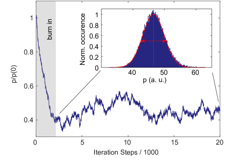
A typical evolution of a single parameter normalized to its starting value is shown in Fig. 6 as a function of the iteration number. In the initial period, the parameters evolve towards the region of a better model representation of the data (higher likelihood) before it settles to a stochastic walk around a particular value (thermalization). The iteration steps before reaching this point are dropped when later examining the distribution of values, and are referred to as the ”burn-in region” Robert (2015); Bolstad (2009). The remaining steps are then processed into histograms for each parameter value, obtaining a marginalized and unnormalized probability distribution for each parameter. We test for an underlying correlation of the steps by only considering every value (thinning). In the last step, the distribution curves are approximated by Gaussians to estimate a mean and a standard deviation for a given parameter based on the data and model used.
VI Mesa Stray fields
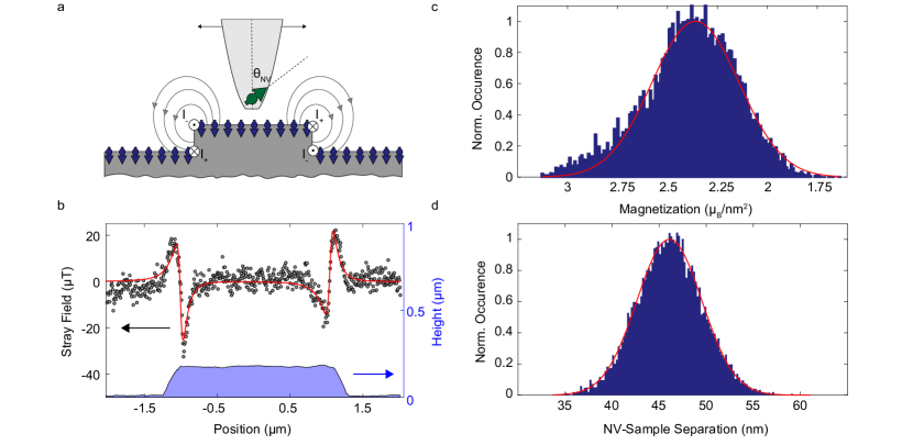
In order to extract quantitative magnetic and sensor information from a mesa, we record its stray field while scanning the magnetometer in a line that crosses the mesa (linecut). This data is then compared to a well-established model tetienne2015 for the stray field of a magnetic stripe, where the field arises from effective currents () running along the top and bottom of its edges as shown in Fig. 7a. According to this model, the stray field measured at a distance from a single edge of a mesa, oriented along the y-axis, is given by:
| (7) | |||||
| and | |||||
| (9) |
Here, is the magnetization, is the thickness of the mesa, is the location of the edge, and are the polar and azimuthal angles of the NV axis respectively and N/A2 is the vacuum permeability. Note that in this configuration. These equations describe the stray fields ( and ) on one side of the mesa, and as such, we add the corresponding terms for the second edge (located at ). In order to take into account a possible asymmetric tip shape or accumulation of dirt during scanning, we allow for two different NV distances ( and ) for either side of the mesa, as described in Rohner et al. (2019).
With this particular analytical form, we now address the recorded stray field data and are left with seven fitting parameters (). In the first step we seek to infer the sensor orientation (,), since we can assume it to be constant throughout all measurements. For this, we perform an initial least-squared fit, seeded from 50 different initial parameter sets and choose the best fit parameters. These parameters, together with the measured stray field values and model described above (Eq. 7), are then used to initialize the MH algorithm (see Section V). From all the combined datasets (29 individual linecuts), we infer the likelihood-distribution of the sensor orientation, by multiplying the individual likelihood distributions of the sensor-angles from each dataset. The resulting distribution is then described by a Gaussian, yielding a and of and respectively.
While there is no reason for and to vary between scans, we can not assume the remaining parameters to stay constant throughout all datasets. Therefore, we proceed with the analysis of individual linescans, with the global sensor orientation as prior knowledge. The 29 individual parameter sets are iterated until the resulting (unnormalized) probability distributions are smooth ( iterations) and approximate them by Gaussians. Note that here, we need to account for the position error arising from the open-loop scanner as described in Section III. This is done by calibrating our length scale and the statements on the error of the individual parameters.
An example of this analysis for the data set in Fig. 7b is shown in Fig. 7(c,d). We approximate each of these histograms with a Gaussian and extract its mean and the standard deviation. For this particular data set, we extract /nm2, nm and nm (not shown). In the main text, we state the mean of obtained at room temperature together with the systematic error.
VII Domain Wall Model
In order to derive a model for the stray field of a domain wall, we consider the surface magnetization of Cr2O3. As for the mesa measurements (Section VI), in our experiments the emerging stray field is measured along the NV axis:
| (10) |
To calculate this field, we use the procedure of propagating fields in Fourier space (with momentum vector q) Dovzhenko et al. (2018), where for a given magnetization , the Fourier components of the magnetic strayfield for a given sensor distance can be calculated with the corresponding propagator :
| (11) |
with:
| (12) |
Here, is the thickness of the magnetic layer and [] is the saturation magnetization. For the two-dimensional surface magnetization, we consider the limiting case such that, is the surface magnetization, and the exponential pre-factor simplifies to .
After an inverse Fourier transformation, one obtains the real-space and components of the stray field of a Bloch wall:
| (13) | ||||
| (14) |
Here, represents the first derivative of the log gamma function. Note that the situation is translation invariant along the y-direction, and therefore produces no stray field in .
In order to validate this analytical description of the stray field of a domain wall, we simulate a Bloch wall in MuMax3 Vansteenkiste et al. (2014).
In the simulation, the surface magnetization of Cr2O3 is approximated by a thin slab given by a single cell with a extent and a magnetization of kA/m , exchange stiffness pJ/m and uniaxial anisotropy of J/m3.
The total dimensions of the simulated sheet are discretized to a grid of cells, including periodic boundary conditions to minimize boundary artifacts.
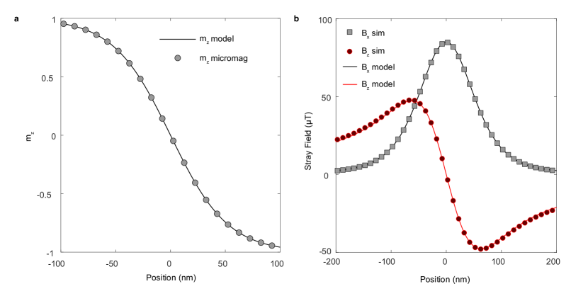
To nucleate a domain wall, we start by considering a sheet magnetized upwards in one half and downwards in the other. After energy minimization of the system via relaxation, a time-span of about is simulated to ensure a static equilibrium. The magnetization profile of the domain wall is then extracted and fitted according to the wall profile described by Eq. (1-3) in the Methods, which yields . In the next step, the stray field at a distance of is extracted from the simulation and compared with Eq. 14. We find very good agreement between the numerical estimates and analytical approximations. In fact, we believe the analytical description to be more accurate in capturing the dipolar stray fields, since the model considers an infinitely extended magnetic system, without the need of periodic boundary conditions or finite extent as present in the simulations. Such a comparison is shown in Fig. 8.
VIII Domain Wall Fitting
Based on concurrent measurements taken over the mesa structures, we can place tight restrictions on the values of , , and . In particular, for , we use the estimate for the larger of the two extracted distances (, , see Section VI) to account for possible dirt when scanning. The scanning direction with respect to our NV axis is readily obtained through our position calibration (Section III), though again, taking into account the error on the angle. This leaves only the domain wall position and magnetic length as complete unknowns.
To proceed, the stray field data of the domain wall, prior information and stray field model (as derived in Section VII) is analyzed via our MH algorithm implementation (Section V). We iterate through steps, resulting in a reasonable modeling of the recorded stray field data, as shown in Fig. 9b and smooth probability distributions for all parameters, in particular for the remaining magnetic length () that determines the width of the domain wall.
The inset of Fig. 9b shows the cumulative distribution function (CDF) of for this data set. The measurement is taken at , and yields a mean magnetic length of with the 2nd and 98th percentiles being and respectively.
We claim that statements on such small () parameters are still reasonable due to the immediate lateral and temporal proximity of the mesa and domain wall measurements. This allows us to assign any broadening in the stray field of the DW, exceeding the expected broadening from the sensor distance , to the domain wall width given by . This is essentially a deconvolution of the domain wall data with the detection function of our setup, possible by the concurrently taken mesa measurement data. The analysis yields our statistical confidence in the model parameters given in the data. In our experience, most systematic errors can be excluded, with the exception of the error arising due to the piezo non-linearity, drift and hysteresis characterized in Section III. We consider the possibilities of these errors in our statement of the DW upper bound by referring to the percentile, while remaining within a reasonable range of values.
IX Temperature Dependence
By mounting the sample on a small Peltier element, we are able to access a range of sample temperatures from room temperature () up to . As such, we are able to explore the temperature dependence of both the sample magnetization and .
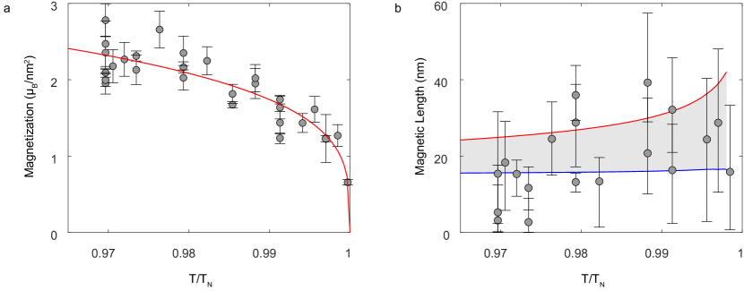
We begin by presenting the magnetization, extracted as described in Section VI, and plotted against the temperature (normalized to the Néel temperature, ) in Fig. 10a. Here, we see that the surface magnetization falls off as
| (15) |
where is the critical exponent. Note that we allow for an offset, of the temperature to take into account a possible calibration offset between the thermistor (which defines ) and the actual sample temperature. Here, we assume the literature value of the Néel temperature (), a reasonable assumption in the absence of excessive strain Kota et al. (2013) or doping Mu et al. (2013), which may lead to changes in . In doing so, we obtain a relatively small offset of only and a critical exponent , well within the range of previously measured values Al-Mahdawi et al. (2017).
Note that the vertical error bars in Fig. 10a are given by the standard deviation of a Gaussian fit to the distribution of , extracted using the MH algorithm. We now repeat the same procedure for , plotted against the temperature in Fig. 10b. Here, the filled circles represent the mean magnetic length extracted from the MH algorithm for each data set. The error bars are given by the 98th (2nd) percentiles of the CDF, to show the maximum (minimum) values of that would be consistent with our data given the constraints we place based on the mesa measurements. In particular, we can look at the room temperature measurements (first three points at the left), which all fall below the 98th percentile bar at . This justifies our statement in the main text, that nm is inconsistent with our measurements at room temperature. Furthermore, we show the theoretical upper (blue) and lower (red) limits given by where is the exchange stiffness and is the anisotropy Foner (1963). In particular, we use the following temperature dependence for Hoser and Koebler (2012); Parthasarathy and Rakheja (2019):
| (16) |
where is the sublattice magnetization and . The exact value of is unknown, but is believed to be close to yielding generally smaller domain wall widths. Furthermore, the value of is estimated as:
| (17) |
with the exchange integral J taken from DFT data Shi et al. (2009b) and being the effective spin length Hoser and Koebler (2012). As such, we see that our measurements are consistent with the theoretical expectations, and expect that, close to the Néel temperature, we would reach a regime where , in which case, we could directly measure . This would require either higher spatial resolution (for lower temperatures) or a higher sensitivity (close to ), which should be achievable in future work.
X Analytics for Snell’s Law
We consider a semi-infinite sample with a mesa of width and thickness on the top surface (). It is assumed that the mesa has a constant rectangular cross-section and is directed along the axis. The continuum model of Cr2O3 can be represented using two antiferromagnetically coupled sublattices with unit magnetization vectors and Samuelsen et al. (1970); Mu and Belashchenko (2019). Within the long-wave approximation, it is reasonable to use the Néel vector order parameter and the total magnetization vector , with and . The latter will be neglected in the following. Then, the effective energy of the sample reads Auerbach (1994); Ivanov (2005)
| (18) |
where is the magnetic length as for the spin-lattice model. Note that additional magnetoelastic terms may be incorporated into the effective value of the anisotropy constant , leading to a shift in with qualitatively identical results Dudko et al. (1971); Gomonay and Loktev (2007); Kota and Imamura (2016). We furthermore assume the exchange-driven Neumann boundary conditions for the Néel vector:
| (19) |
where is the surface normal. In the following, we use the local spherical reference frame parametrization . We set the equilibrium, bulk domain wall position to the plane where is assumed to be small. We also assume a mesa geometry satisfying . Then, we can describe the domain wall as it passes through the mesa through the following Ansatz:
| (20) |
Here, with being the rotation matrix around at an angle , and describes the domain wall profile in bulk and mesa, respectively. We use
| (21) |
with . The values of and are determined through the energy minimization below. The function is determined by minimizing the energy functional (18) within the mesa and reads
| (22) |
where and we set . Then, the total energy of the domain wall (), up to a constant, reads:
| (23) | ||||
where is the value of the Riemann zeta-function and is chosen from condition . The value of from Eq. (21) is thereby given by . This parameter plays a particularly important role as it determines the length scale over which inhomogeneities in the domain wall persist into the bulk below the mesa. For this reason, we rename this parameter as in the main text. Furthermore, characterizes the direction of the domain wall at the bulk-mesa interface. Note, that it is dependent only on the mesa aspect ratio, which allows us to scale simulations for direct comparison with experiment.
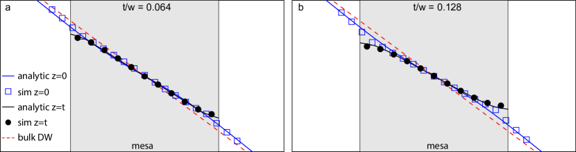
In particular, Fig. 11 shows the comparison between the analytics developed here (solid black and blue lines) and simulations (black circles and blue squares, where we see excellent agreement. In both analytics and simulation, we see the S-shaped bending of the domain wall on the mesa and the gradual twisting of the domain wall to match that of the bulk position (red dashed line) as we go into the bulk. The S-shaped deviation is much less pronounced for thinner mesas (Fig. 11a), which is very similar to the experimental case.
The Snell’s law for the domain wall can be determined using the equilibrium domain wall profile in bulk and at the mesa top surface (). The incidence angle is given by , while the refraction angle can be estimated as with . Then,
| (24) |
XI Elastic Properties of the Domain Wall
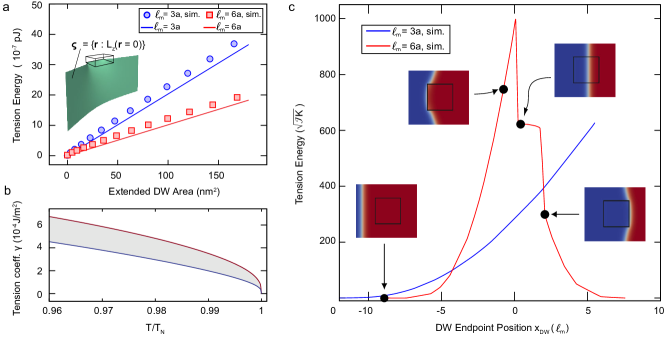
In experiments and simulations, we have observed a behavior of the DW that mimics that of a rubber band. As such, we describe the DW trajectory and interactions with the mesa using its elastic properties, that is, the DW surface energy and corresponding surface tension. In particular, we can consider the surface where the Néel order parameter lies horizontally (), and use this to describe the DW. We can address the details of by means of spin lattice simulations (see Simulation Details in the main text for more details). In Fig. 2c of the main text, we see that the domain experiences the strongest deflection at the edge of the mesa when crossing from bulk to mesa. As previously discussed, this behavior is well-described by the Ansatz in Eq. 20, where the parameter determines how far the wall is deflected in the plane of the mesa and (introduced in Eq. 21) characterizes the deflection in the vertical direction. The same behavior exists in the case where the domain wall is deformed around the mesa, as shown in the inset of Fig. 12a. Here, exhibits a smooth bend deep in the bulk and sharper deflections near the mesa edges. The additional, tensional energy due to this bending is plotted here for two different values of (circles and squares) as a function of the increase in area DW area arising from the bending. We can compare the results of these simulations with analytical calculations if we assume that the inhomogeneities of are gradual, i.e. have a radius of curvature larger than . In this case, we can describe the DW’s mechanical tension by:
| (25) |
Here, we have defined a tension coefficient for the DW, which is plotted in Fig. 12a as solid lines for two different values of .
We can furthermore explore the impact of temperature on the tension coefficient. To do so, we use the temperature dependence of Hoser and Koebler (2012); Parthasarathy and Rakheja (2019) and Foner (1963), as in Fig. 10b. The corresponding upper and lower bounds of the tension coefficient are then shown in as shown in Fig. 12b, where the observed reduction in with increasing temperature implies an increase in elasticity, or a ’DW softening’. The consequences of this are more clear in Fig. 12c. Here, we show the pinning surface (tension) energy of the domain wall as a function of the DW position relative to a mesa, as in Fig. 3c in the main text, for two different values of . As increases with increasing temperature, this acts as an effective tuning parameter for the temperature in these simulations. The blue curve is as shown in Fig. 3c, where the DW deforms continuously. However, for larger (red), i.e. higher temperatures, we see a different pinning behavior, illustrated with the snapshots inset to the figure. Here, the DW is first deformed around the mesa, before snapping into a straight configuration, passing through the mesa. As the DW is moved closer to the opposite edge of the mesa, the mesa will again be preferentially pinned to the mesa edge for some distance, on the order of , at which point the DW no longer feels the influence of the mesa. Thus, we expect that the pinning of the DW can be strongly influenced by temperature. However, this reduction in pinning strength can be overcome by carefully tuning the mesa geometry.
XII Domain Wall Dragging
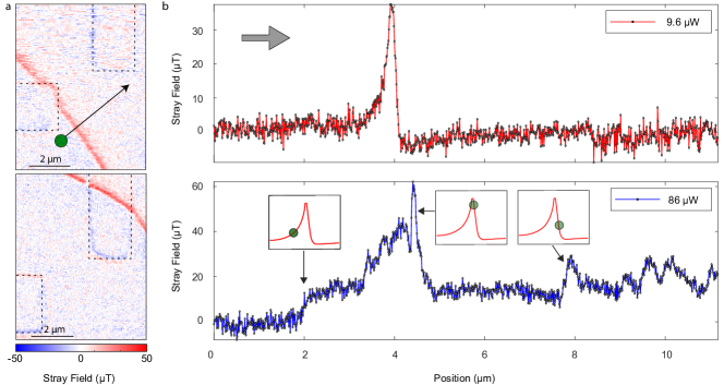
We are able to explain dragging of the domain wall by the laser through the formation of an effective attractive potential for the DW by local heating. Heating of the sample appears to lower the effective depth of pinning potentials, evidenced by the fact that reproducible laser dragging is only achieved at sample temperatures above room temperature, and near . The additional heating provided by the laser then allows us to completely overcome this barrier, and move the domain wall freely. However, once the heating, i.e. laser, is removed, the domain wall tension causes the wall to snap back to its original position unless it becomes pinned along the way. This dragging and pinning can also be achieved over m-scale distances, as shown in Fig. 13a, where we drag the DW using the same technique outlined in the main text, over a distance of . This implies that every time we observe a movement of the DW, we are moving it between strong pinning sites, which can be internal crystal defects or fabricated surface structures.
We support these claims by further scans across the domain wall with the NV scanning probe at increased laser intensities. In this way, we aim to heat the sample with the near-field of the excitation laser near the tip of the scanning probe while simultaneously measuring the stray field from the DW at the NV position. An example of this procedure is shown in Fig. 13b, where we compare the measured stray field at low power ( - red) and high power ( - blue) laser excitation (with powers measured at the rear lens of the microscope objective). Each scan is performed with a integration time per point, over the same section of domain wall, at a global sample temperature of 304.5 K. At low power, we see a domain wall stray field as already discussed. Increasing the power results in additional peaks in occurring at erratic locations. We explain this observation with a number of pinning sites located along the DW path as the DW is bent by laser dragging. In particular, we see an initial increase and plateau in , which is consistent with an attractive potential moving the domain wall ahead of the NV position. The field then increases, meaning that we pass over the domain wall with the NV, which can only be achieved by pinning of the domain wall. However, at some point, the pinning is overcome and the domain wall is again dragged together with the laser. We furthermore see a number of smaller pinning centers, evidenced by the slight peaks in field towards the end of the scan. In the insets of Fig. 13b, we show the position of the NV relative to the stray field pattern that would result in such peaks. Furthermore, as we continue to observe a non-zero stray field while scanning, we expect that the sample temperature surrounding the NV is still below . If we again image the domain wall at low green laser power after such dragging, we see that the position remains unchanged in most cases. This indicates that the other pinning centers we observed are rather weak, and are overcome by the domain wall tension. Thus, we can directly observe the dragging of the domain wall by the laser and thereby gain information about the pinning landscape in the sample - a potential avenue for future research.