Flux periodic oscillations and phase-coherent transport in GeTe nanowire-based devices
Abstract
Despite the fact that GeTe is known to be a very interesting material for applications in thermoelectrics and for phase-change memories, the knowledge on its low-temperature transport properties is only limited. Here, we report on phase-coherent phenomena in the magnetotransport of GeTe nanowires. From universal conductance fluctuations, a phase-coherence length of about 200 nm at 0.5 K is determined for the hole carriers. The distinct phase-coherence is confirmed by the observation of Aharonov–Bohm type oscillations for magnetic fields applied along the nanowire axis. We interpret the occurrence of these magnetic flux-periodic oscillations by the formation of a tubular hole accumulation layer on the nanowire surface. In addition, for Nb/GeTe-nanowire/Nb Josephson junctions, we obtained a proximity-induced critical current of about 0.2 A at 0.4 K. By applying a magnetic field perpendicular to the nanowire axis, the critical current decreases monotonously with increasing magnetic field, which indicates that the structure is in the small-junction-limit. Whereas, by applying a parallel magnetic field the critical current oscillates with a period of the magnetic flux quantum indicating once again the presence of a tubular hole channel.
I Introduction
In the past decades, GeTe-based alloys are attracting an increasing interest for their applications in optical data storage and phase change memories due to a reversible rapid transformation between amorphous and crystalline phaseWuttig and Yamada (2007); Lencer et al. (2008) and a large contrast of optical constants and electrical conductivity for the two phases.Guo et al. (2015) In addition, GeTe-rich alloys can be used in intermediate temperature thermoelectric applications for converting waste heat to electrical energy because of their high thermoelectric performance, high thermal and mechanical stability.Hong et al. (2019); Perumal et al. (2016) Moreover, the GeTe ferroelectric semiconductor exhibits a giant bulk Rashba effect,Pawley et al. (1966); Ponet and Artyukhin (2018); Liebmann et al. (2016); Krempaský et al. (2020) which is very interesting for applications in spintronic devices. Di Sante et al. (2013); Bahramy and Ogawa (2017)
It is well known that GeTe has different phases upon increasing the temperature or pressure.Singh (2013); Hong et al. (2019); Pawbake et al. (2019) At room temperature, GeTe is an indirect band gap semiconductor with a trigonal ferroelectric phase (space group , No. 160). The experimentally determined band gap energy is 0.61 eV,Park et al. (2008) which is close to recent theoretical values.Di Sante et al. (2013); Singh (2013) The band gap energy tends to decrease with decreasing temperature.Hong et al. (2019) Pristine GeTe is a -type semiconductor with hole concentration up to 1021 cm-3 due to the low formation energy of Ge vacancies.Hong et al. (2019) At temperatures below 0.3 K GeTe is observed to be The superconducting.Hein et al. (1964); Smith and Stiles (1977); Narayan et al. (2016) Recently, Narayan et al.Narayan et al. (2019) have investigated the non-equilibrium superconductivity in GeTe Hall bar samples with a semiconductor-superconductor transition temperature of about 0.14 K and a critical magnetic field of around 70 mT. At the Curie temperature of about 700 K, GeTe undergoes a phase transition from the ferroelectric rhombohedral () structure to the paraelectric cubic () NaCl-type one. The cubic GeTe has a direct band gap with a smaller value of about 0.2 eV.Singh (2013); Tsu et al. (1968) In addition, there is an amorphous (high-resistance phase) to crystalline (low-resistance phase) transition at around 200 ∘C for GeTe films upon heating.Andrikopoulos et al. (2006); Guo et al. (2017) For device applications investigations on GeTe nanowires were conducted.Meister et al. (2006, 2008); Longo et al. (2011) These nanowires are in particular interesting as building blocks in phase-change memories.Lee et al. (2007)
The mechanism of low-temperature quantum transport phenomena in one-dimensional GeTe nanowires have not been addressed so far, even though the phase change behavior and thermoelectric properties of GeTe bulk/films have been studied systematically. Therefore, we have grown GeTe nanowires and measured the transport properties of GeTe nanowires contacted with normal metals as well as GeTe nanowire-based Josephson junctions. For the normal contacted nanowires we investigated phase-coherent transport phenomena such as universal conductance fluctuations, weak antilocalization, as well as Aharonov–Bohm-type resistance oscillations. For the GeTe nanowires equipped with Nb contacts the proximity-induced superconductivity as well as critical temperature and magnetic field of Nb/GeTe-nanowire/Nb Josephson junctions are studied.
II Results and Discussion
II.1 Crystalline structure and microstructure analysis
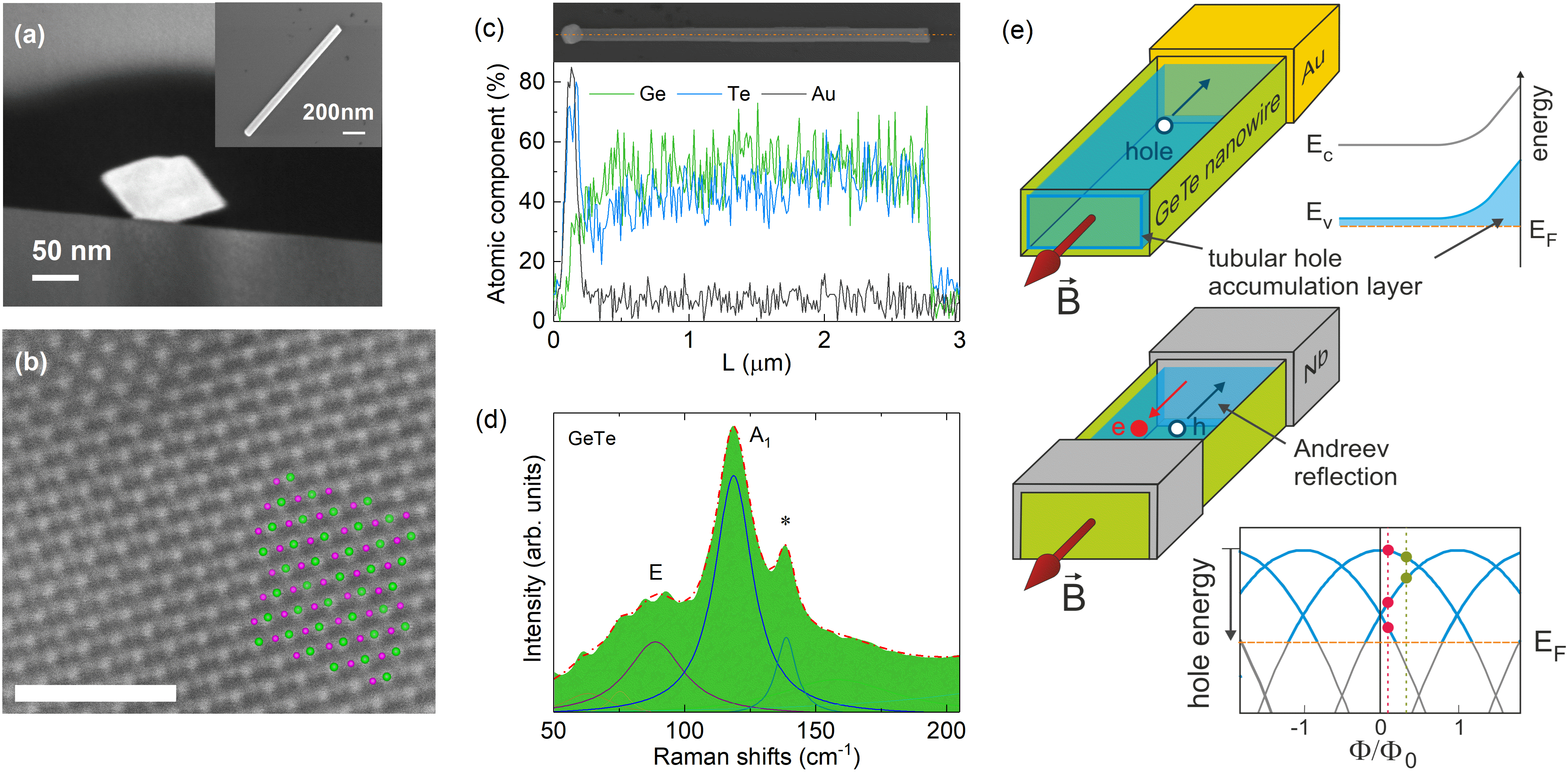
GeTe nanowires (NWs) were synthesized by a Au-catalyzed vapor-liquid-solid growth in a tube furnace with GeTe powders.Meister et al. (2006); Yu et al. (2006) The as-grown GeTe NWs on a Si/SiO2 substrate are straight with a length of more than 5 m. The cross section for the GeTe nanowires has a rhombic shape with a side length of about 80 nm (cf. Figure 1a). A high-angle annular dark- field (HAADF) image of GeTe NW cross section was obtained via aberration corrected scanning transmission electron microscopy (STEM). In the corresponding image shown in Fig. 1b one can identify a trigonal crystal structure. The positions of the Te and Ge atoms are indicated by light green and magenta dots, respectively. For device fabrication the GeTe NWs were transferred to a Si/SiO2 substrate. Subsequently, superconducting (Nb) or normal-metal (Ti/Au) contact electrodes were prepared by using electron beam lithography and magnetic sputtering. The transport properties of Nb/GeTe/Nb and Au/GeTe/Au devices are studied in a four-terminal configuration. The outer pair of electrodes are employed to apply a direct current () or/and an alternating current (), while the inner pair of leads serve as voltage probes. The contact resistance can be excluded using a real four-terminal geometry base on the differential resistance Skryabina et al. (2017).
In order to investigate the material properties of the nanowires energy dispersive X-ray spectroscopy (EDX) and Raman spectroscopy were performed. The EDX results shown in Figure 1c reveal that the as-grown GeTe has an ideal atomic ratio of Ge : Te = 1 : 1 and the element component are uniform along the NWs except the nanowire ends with a Au nanoparticle, typical of vapor-liquid-solid growth. Furthermore, Raman spectra of a GeTe single nanowire demonstrate unambiguously that GeTe NWs exhibit rhombohedral phase (R3m) at room temperature (cf. Figure 1d). According to the group theory, the two peaks near 89 and 119 cm-1 are assigned to the first-order Raman-active modes E(TO) and A1(LO), respectively.Bragaglia et al. (2016); Shaltaf et al. (2009) Theoretically, E and A1 relates to the bending modes of the GeTe4 tetrahedra and symmetric stretching vibration of the Te-Te bond, respectively.Andrikopoulos et al. (2006) Note that the peak labeled by the symbol () at around 140 cm-1 arises from surface oxidation.Pawbake et al. (2019) Other peaks/shoulders may originate from the breaking of inversion symmetry due to vacancies, defects, and distortion of bonds.Shalini et al. (2015)
II.2 Magnetotransports in normal-metal Au/GeTe-nanowire/Au devices
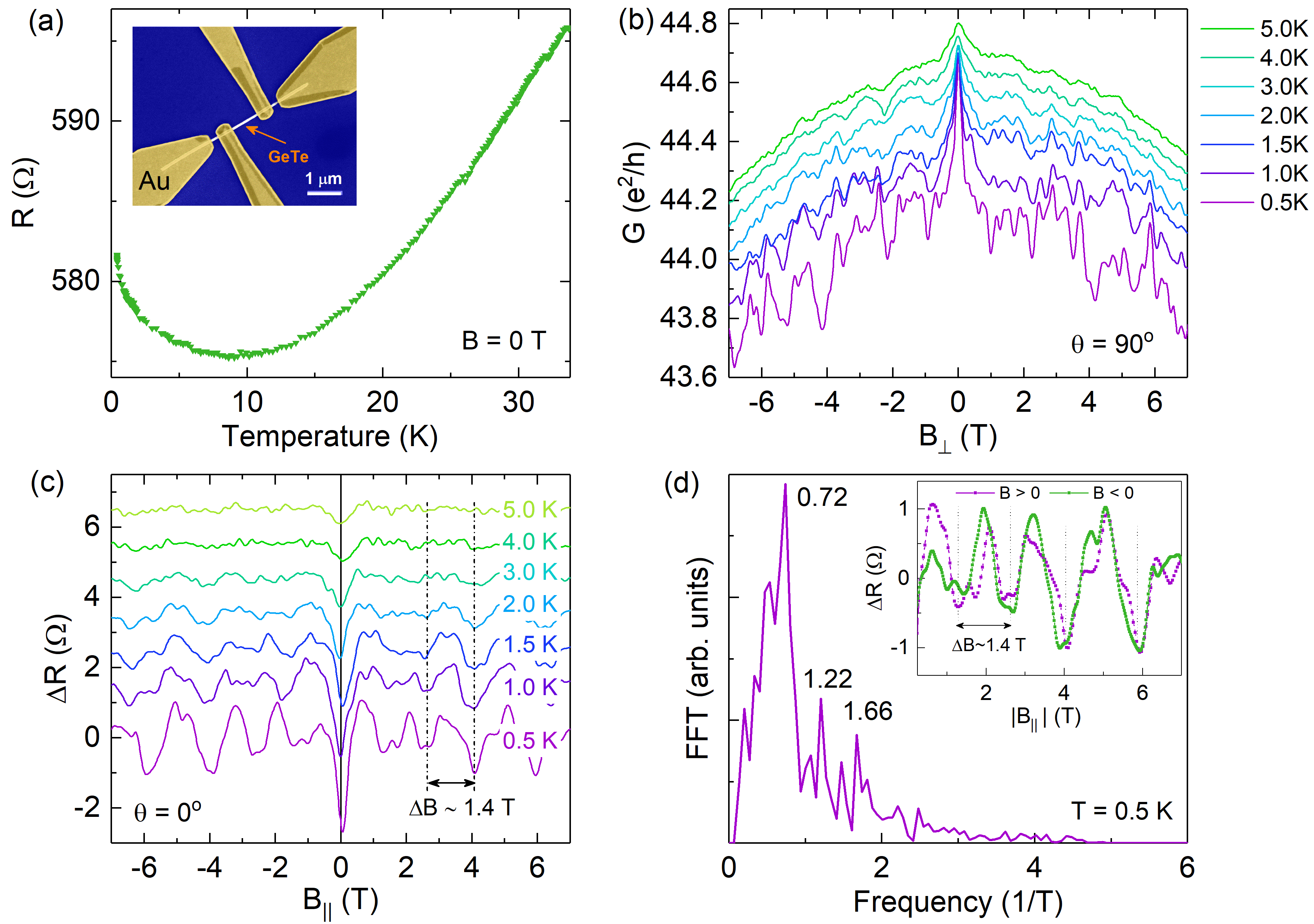
In order to gain information on the electrical properties of the GeTe nanowires we measured the magnetotransport of samples equipped with normal contacts (Ti/Au: 20 nm/100 nm). An electron beam micrograph of the contacted 80-nm-wide nanowire is shown in Figure 2a (inset). The measurements were performed in a four-terminal configuration with the bias current supplied at the outer contacts. The width and separation of the inner electrodes is about 0.5 and 1.0 m, respectively. In Figure 2a the resistance as a function of temperature is plotted. One finds that the resistance decreases with decreasing temperature in the temperature range from 35 to 10 K, and then increases monotonously upon further decrease of the temperature down to 0.4 K. The temperature dependence corresponds to a metallic behaviour where the upturn in resistance for temperatures below 10 K can be attributed to the electron-electron interaction and weak localization effects.Weyrich et al. (2016); Lee and Ramakrishnan (1985); Bergmann (1984) No transition to a superconducting behaviour is observed, probably because the lowest temperature of 0.4 K is larger than the critical temperature.Hein et al. (1964); Narayan et al. (2016)
Figure 2b shows the conductance in units of with the magnetic field applied perpendicular to the nanowire axis (B⟂, = 90∘), at temperatures between 0.5 and 5.0 K. Here, is the electron charge and is the Planck constant. Similarly to GeTe films,Narayan et al. (2016) a pronounced peak is observed at zero magnetic field which is attributed to the weak antilocalization effect. This feature originates from interference effects of holes in the presence of spin-orbit coupling. Indeed, for GeTe a bulk Rasbha effect in the valence band is theoretically predicted.Di Sante et al. (2013); Liebmann et al. (2016) Furthermore, as discussed in more detail below, band bending at the surface in connection with according potential gradients may also result in spin-orbit coupling effects. The conductance traces shown in Figure 2b reveal a modulation pattern which can be assigned to universal conductance fluctuations.Lee and Stone (1985) Their amplitude decreases with increasing the temperature mainly due to the reduction of the phase-coherence length.Arango et al. (2016) From the autocorrelation function of the magnetoconductance, given by , information on the phase-coherence length can be obtained.Lee and Stone (1985) Here, is the average over the magnetic field. For quasi one-dimensional systems the correlation field defined by , is inversely proportional to the phase-coherence length : , with the magnetic flux quantum given by = .Ferry et al. (2009); Beenakker and van Houten (1991) For the fluctuations measured at 0.5 K, we extracted a correlation field of T. Taking the nanowire width of 80 nm into account we obtain a phase-coherence length of about 200 nm.
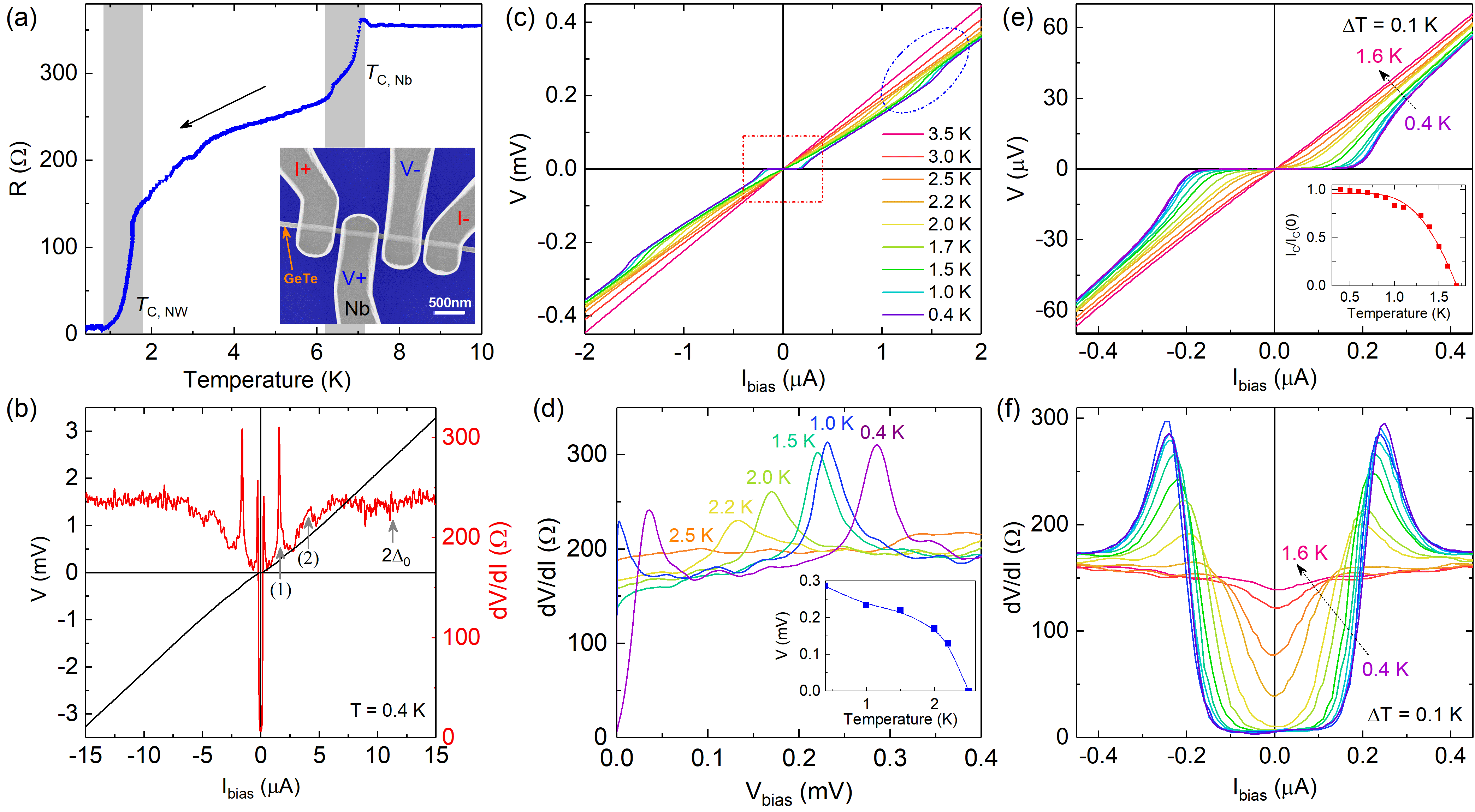
Figure 2c shows the resistance after subtraction of a slowly varying background as a function of a magnetic field applied along the nanowire axis. For this magnetic field orientation one finds a regular oscillation pattern with an oscillation period of about T (cf. Figure 2d, inset). This is also confirmed by the fast Fourier spectrum of the measurement at 0.5 K depicted in Figure 2d. Here, a pronounced peak is found at a frequency of 0.72 T-1, corresponding to the aforementioned period of 1.4 T. In addition, some features at 1.22 and 1.66 T-1 are present.
We attribute the regular oscillations to Aharonov–Bohm type oscillationsAharonov and Bohm (1959) originating from transport in tubular hole states in a conductive surface accumulation layer penetrated by a magnetic flux (cf. Fig. 1e, upper left schematics).Richter et al. (2008); Peng et al. (2010); Gül et al. (2014); Cho et al. (2015); Arango et al. (2016) The involvement of phase-coherent tubular states is supported by the large phase-coherence length being comparable to the circumference of the nanowire. We assume that in case of our GeTe nanowire, the holes accumulated in the surface channel are supplied from surface states. In fact, such a surface accumulation layer is mainly observed for narrow band gap materials, e.g. for InAs. Similar but inverted as in the case of InAs the GeTe electronic band structure exhibits some lower valence band maxima,Polatoglou et al. (1982); Jain et al. (2013) which may be responsible for the charge neutrality level of the surface states to be located within the bulk valence band. As a consequence, a tubular hole accumulation layer is formed at the surface.Lüth (2015) Owing to the hole accumulation the valence band is bent upwards at the interface (cf. Fig. 1 e). In order to describe the transport through the tubular hole channel in more detail, we assume a circular cross section. In that case the state components perpendicular to the nanowire axis can be described by coherent angular momentum states, which can be ordered according to their angular momentum quantum number of their angular momentum . In the presence of a magnetic flux through the wire cross section the energy eigenstates are given byRichter et al. (2008); Gül et al. (2014)
with the kinetic energy along the wire, the effective hole mass, and the radius of the tubular channel. The energy is periodic in . A schematics of the energy spectrum is given in Figure 1e, bottom. In a ballistic picture the conductance is determined by the number of occupied hole channels above the Fermi level , e.g. three channels for a small flux (red dots in the schematics) and two channels for a slightly larger flux (green dots).Richter et al. (2008) Thus, when the magnetic field is increased, the number of occupied hole channels changes periodically with the period of . In the non-ballistic diffusive case, a similar flux-periodic modulation is expected as well.Rosdahl et al. (2014)
From the measured period of T of our nanowire we can deduce the expected area encircled by the surface channel from , which results in a value of about , corresponding to a diameter of approximately 60 nm for a circular cross section. For our nanowire with a width of nm, we estimate an area of about assuming a circular cross section. Obviously, the expected cross section is smaller than the actual geometrical cross sectional area of our GeTe nanowire. The discrepancy may be attributed to the fact that the nanowire surface is oxidized so that the hole accumulation layer is slightly pushed inside. Furthermore, the radial component wave function usually has an extension of the few nanometers, which also leads to a reduction of the effective cross sectional area. As mentioned above, some weaker maxima at higher frequencies, i.e. at 1.22 and 1.66 , are found in the Fourier spectrum. These features may be related to higher harmonics or to Altshuler–Aronov–Spivak oscillations comprising a periodicity.Al’tshuler et al. (1981)
II.3 Temperature dependent superconductivity in Nb/GeTe-nanowire/Nb junctions
We now turn to measurements of GeTe nanowires equipped with superconducting contacts. The inset of Figure 3a shows a GeTe NW-based junction device with Nb contacts. The nanowire has a width of 80 nm, while the width and separation of Nb leads are about 500 and 90 nm, respectively. The outer Nb leads are employed to apply bias current, while the inner pair of contacts serve as voltage probes.Courtois et al. (1995) Figure 3a shows the resistance at zero magnetic field as a function of temperature. The measurement shown in Figure 3a indicates that the Nb electrodes have a transition temperature of about = 7.0 K. From the relation of the electron-phonon coupling strength 3.9, with the Boltzmann constant and critical temperature , we estimate the Nb energy gap to be about 1.2 meV at zero temperature.Carbotte (1990); Günel et al. (2012) Moreover, there is another drop in the temperature region between 1.0 and 2.0 K, which is assigned to the superconducting transition temperature of the Nb/GeTe-NW/Nb junction. The two-step feature has been observed before in normal metal,Angers et al. (2008) in semiconductor-based Josephson junctions,Kim et al. (2017) as well as in topological insulator based junctions.Zhang et al. (2020) The normal state four-terminal resistance () of the present Nb/GeTe-NW/Nb junction is about 355 at temperatures above .
Figure 3b shows the current-voltage (I-V) characteristics and corresponding differential resistance (dV/dI) curve measured at 0.4 K. At low bias currents a superconducting state is observed with a critical current of 200 nA. At larger bias current at around 1.6 A corresponding to a bias voltage of about 0.3 mV a sharp peak (1) is observed in the differential resistance. Moreover, a broader peak (2) at 4 A corresponding to a bias voltage of 0.75 mV is found. These features can be attributed to multiple Andreev reflections.Octavio et al. (1983) However, no regular sequence of structures according to the theory is observed. At a bias voltage corresponding to meV no pronounced feature is found.
As a further step, the temperature dependence of the I-V characteristics is investigated (cf. Figure 3c). Obviously, the superconducting range at small bias currents (indicated by a rectangle) shrinks and finally vanishes upon increasing the temperature from 0.4 to 3.5 K. The same is true for the step feature at around 1.5 A. Regarding the latter, the corresponding dV/dI traces as a function of bias voltage are shown in Figure 3d for temperatures in the range from 0.4 to 2.5 K. One finds that the feature corresponding to peak (1) in Fig. 3b shifts towards smaller bias voltages and eventually vanishes at a temperature of 2.5 K (cf. Figure 3d, inset). The strong temperature dependence confirms that this feature is directly related to the superconducting state.
Figure 3e shows the I-V characteristics of the GeTe-NW based Josephson junction in a small bias current range at temperatures ranging from 0.4 to 1.6 K. At 0.4 K the critical current is about 200 nA. As the temperature increases, the superconducting plateau diminishes and disappears at about 1.6 K. The according corresponding differential resistance traces are shown in Figure 3f. The dependence of normalized critical current (0) as a function of temperature are depicted in the inset of Figure 3e. The temperature dependence of the supercurrent can be assigned to a metallic diffusive junction.Dubos et al. (2001) However, since no reliable data on the diffusion constant and Thouless energy can be obtained, we have refrained from a detailed analysis.
II.4 Magnetic field dependent superconductivity in Nb/GeTe-NW/Nb junctions
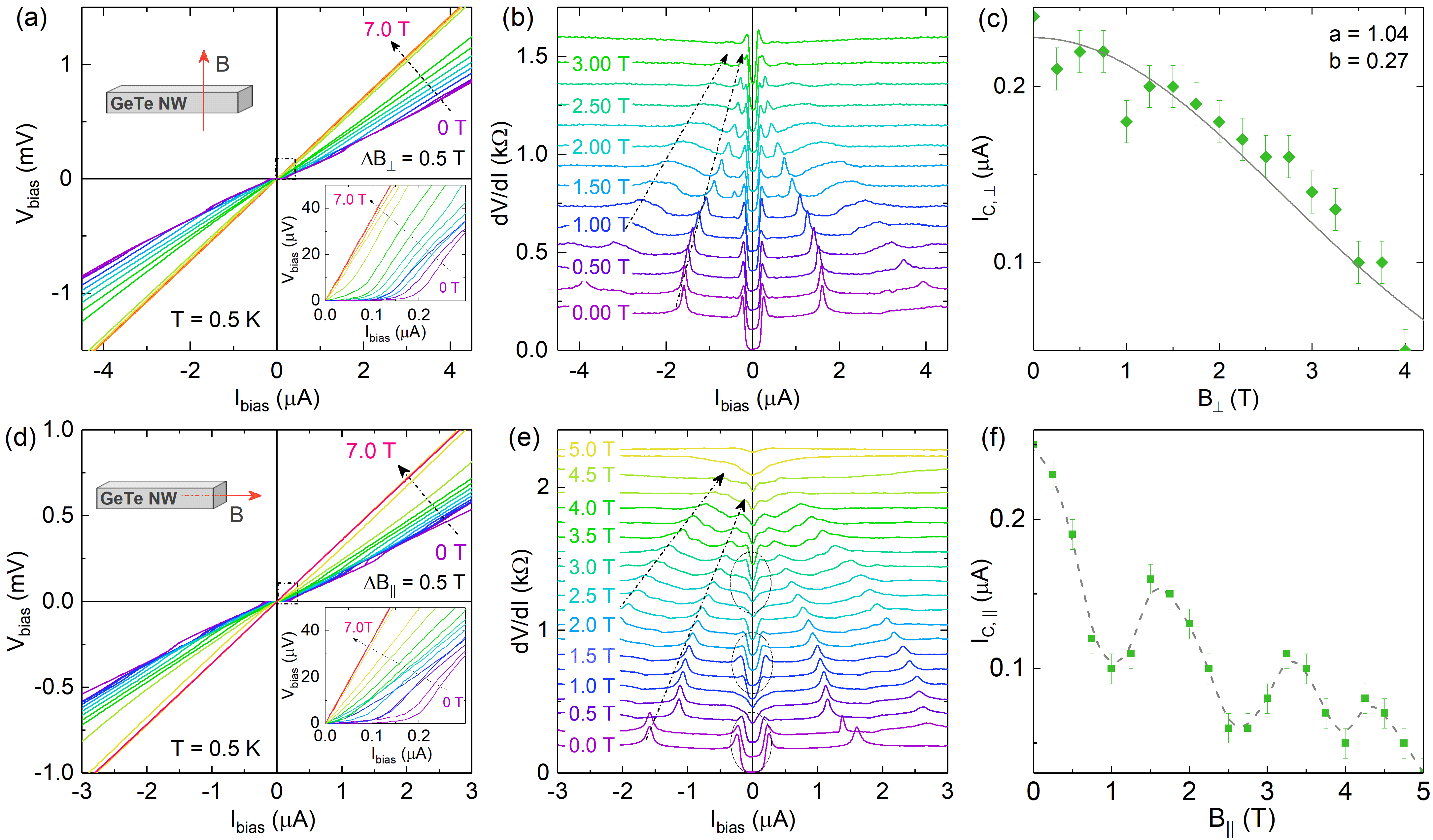
The Nb/GeTe-NW/Nb junctions were measured in a magnetic field in two orientations, i.e. parallel to the nanowire axis and perpendicular to the substrate plane. For the perpendicular configuration the critical field was determined to be around 4 T while for the parallel case we got T. Figures 4a and 4b depict the evolution of I-V and corresponding dV/dI characteristics of the Nb/GeTe-NW/Nb junction in a perpendicular magnetic field (B⟂) at 0.5 K. With increasing magnetic field, the supercurrent is suppressed and then disappears, as can be seen in more detail in Figure 4a (inset). The features at around 1.6 and 4 A found in the dV/dI trace at zero field shift towards zero bias upon increasing the magnetic field. The shift can be attributed to the reduced superconducting gap when a magnetic field is applied. As shown in Figure 4c, we find a monotonous decrease of the critical current Ic,⟂ with increasing . A complete suppression of Ic,⟂ occurs at around 4 T. A similar monotonous decrease of critical current with was observed in planar Nb/Au/NbAngers et al. (2008) as well as in semiconductor nanowire based Josephson junctions.Frielinghaus et al. (2010); Günel et al. (2012) It can be explained within the framework of a theoretical model for the proximity effect in diffusive narrow-width Josephson junctions.Cuevas and Bergeret (2007) Within that model the decay of can be described by:Cuevas and Bergeret (2007); Angers et al. (2008) . Here, is the critical current at T. The a and b are fit parameters and S is the effective area (80 nm90 nm) of the Nb/GeTe/Nb junction perpendicular to magnetic field. The fit curve from theory (solid line) agrees well with the experimental data for fit parameters a and b of 1.04 and 0.27, respectively.
In the case that the applied magnetic field is parallel to the GeTe wire axis (B||), the supercurrent is modulated when the magnetic field is increased, as can be seen in Figures 4d and 4e. Furthermore, similar to the previous case where was applied the peak features in the traces shift towards zero bias upon increasing of . In Figure 4e the ranges where a Josephson supercurrent is present is indicated. The corresponding values of as a function of B|| are plotted in Figure 4f. One clearly finds an oscillatory behaviour of . The oscillation period of is very similar to the period of the sample with normal contacts as discussed before. Since the cross section of the nanowire is very similar to the previous one, we can deduce that oscillations of are periodic with a single magnetic flux quantum . We interpret the behaviour by a Josephson supercurrent which is carried by coherent closed-loop states in the surface accumulation layer at the GeTe nanowire surface. As illustrated in Fig. 1e, bottom, the supercurrent originates from phase-coherent Andreev retro-reflections of tubular hole and electron states at both GeTe/Nb interfaces.Kulik (1969) In each cycle a Cooper pair is effectively transported from one Nb electrode to the other one. In the measurements of GeTe nanowire with normal contacts we found that the resistance was modulated with a magnetic flux quantum because of the periodic change of the number of occupied transport channels. In case of superconducting electrodes, the magnitude of the Josephson supercurrent is also considered to be determined by the number of hole and electron transport channels, hence a flux periodic modulation is expected as well. As a matter of fact, a magnetic flux modulation was found before in junctions based on GaAs/InAs core/shell nanowires.Gül et al. (2014); Haas et al. (2018) However, in that case no clear supercurrent was observed and a period of was found.
III Conclusion
In summary, magnetotransport of GeTe nanowire-based devices have been investigated in a four-terminal configuration. The temperature dependent resistance of the normal metal contacted Au/GeTe-nanowire/Au devices reveals that GeTe exhibits a semiconducting behavior until 0.4 K. At low temperatures universal conductance fluctuations were observed which allowed us to extract the phase-coherence length being as large as 200 nm at 0.5 K. The weak antilocalization feature observed around zero magnetic field indicates the presence of spin-orbit coupling in the valence band. Even more, when a parallel magnetic field is applied regular Aharonov–Bohm type oscillations are found, which are attributed to the formation of a hole accumulation layer at the nanowire surface. In the case of Nb/GeTe-NW/Nb junctions, we observed a critical supercurrent of about A at 0.4 K. The temperature dependence of can be explained in the framework of a diffusive junction. With increasing a perpendicular magnetic field the critical current decreases monotonously. This feature can be explained within models covering the small junction limit. For magnetic fields applied parallel to the nanowire axis regular oscillations of the critical current are observed which are attributed to a supercurrent carried by the surface accumulation layer in the GeTe nanowires.
Our investigations showed that distinct phase-coherent phenomena can be observed in GeTe nanowire structures. The presence of spin-orbit coupling in combination with the superconducting proximity effect make these nanowires very attractive for applications in the field of quantum computation. Furthermore, it would be very interesting to measure the bulk Rashba effect in connection with the ferroelectric properties under a gate bias.
IV Experimental Details
GeTe nanowire synthesis: The synthesis of GeTe nanowires are achieved by a Au-catalyzed vapor-liquid-solid growth. Firstly, the Si(100) substrates with a native oxide were cleaned with acetone, iso-propyl alcohol, and deionized water in an ultrasonic cleaning bath, and then treated in a piranha solution to remove organic residues. After that, the substrates were immersed in Au nanoparticles solution for a few min and rinsed with deionized water. Finally, bulk GeTe (99.99%, Sigma-Aldrich) was evaporated at the center of a horizontal tube furnace, and the reaction product was collected downstream on a Si/SiO2 substrate covered with colloidal Au nanoparticles. Specifically, the furnace was evacuated and purged three times with Ar gas. Then it was heated to 400 ∘C and persisted for 8 h. During this program, the Ar flow rate and the pressure in the quartz tube were about 140 sccm and 10 Torr, respectively.
GeTe-based device fabrication: In order to contact a single GeTe nanowire with Nb or Au electrodes, the as-grown GeTe NWs were transferred to a Si/SiO2/Si3N4 substrate with predefined markers for electron beam lithography. A two-layer (copolymer/950K) polymethyl methacrylate (PMMA) resist system was adopted to realized an ideal shape of Nb or Au leads. In order to obtain a transparent interface between electrodes and GeTe, the samples were exposed to an oxygen plasma to remove resist residues on the contact area. Before the deposition of the electrodes on a single nanowire in a magnetron sputter chamber with a DC power of 250 W, the samples were lightly cleaned by 45 s Ar+ plasma milling to remove native oxidation layers on the GeTe surface.
Morphology and composition characterizations: The morphology and chemical composition of the GeTe nanowires was determined by SEM and EDX, respectively. In addition, a cross sectional specimen has been prepared by focused ion beam techniques. High-angle annular dark field imaging in the STEM has been employed to investigate the cross sectional shape of the nanowires. In addition, the crystalline structure has been investigated by x-ray diffraction and Raman scattering.
Magnetotransport measurements: The temperature and magnetic field dependent I-V characteristics and dV/dI curves were measured using a standard lock-in technology in a 3He cryostat with a base temperature of 0.4 K and a magnetic field range from to 8 T. A four-terminal current driven geometry is employed to directly measuring the voltage drop across the inner section of GeTe nanowire between the nearest internal electrodes. The external pair of electrodes was used for current bias.Zhang et al. (2020) The differential resistance (dV/dI) is gained by superimposing a small AC current of 10 nA at 9.4 Hz on a DC bias current. Note that the applied bias current should be as small as possible to avoid electron heating and damage of the GeTe-based nanodevices.
References
- Wuttig and Yamada (2007) M. Wuttig and N. Yamada, Nat. Mater. 6, 824 (2007).
- Lencer et al. (2008) D. Lencer, M. Salinga, B. Grabowski, T. Hickel, J. Neugebauer, and M. Wuttig, Nat. Mater. 7, 972 (2008).
- Guo et al. (2015) S. Guo, X. J. Ding, J. Z. Zhang, Z. G. Hu, X. L. Ji, L. C. Wu, Z. T. Song, and J. H. Chu, Appl. Phys. Lett. 106, 052105 (2015).
- Hong et al. (2019) M. Hong, J. Zou, and Z.-G. Chen, Adv. Mater. 31, 1807071 (2019).
- Perumal et al. (2016) S. Perumal, S. Roychowdhury, and K. Biswas, J. Mater. Chem. C 4, 7520 (2016).
- Pawley et al. (1966) G. S. Pawley, W. Cochran, R. A. Cowley, and G. Dolling, Phys. Rev. Lett. 17, 753 (1966).
- Ponet and Artyukhin (2018) L. Ponet and S. Artyukhin, Phys. Rev. B 98, 174102 (2018).
- Liebmann et al. (2016) M. Liebmann, C. Rinaldi, D. Di Sante, J. Kellner, C. Pauly, R. N. Wang, J. E. Boschker, A. Giussani, S. Bertoli, M. Cantoni, L. Baldrati, M. Asa, I. Vobornik, G. Panaccione, D. Marchenko, J. Sánchez-Barriga, O. Rader, R. Calarco, S. Picozzi, R. Bertacco, and M. Morgenstern, Advanced Materials 28, 560 (2016).
- Krempaský et al. (2020) J. Krempaský, M. Fanciulli, L. Nicolaï, J. Minár, H. Volfová, O. c. v. Caha, V. V. Volobuev, J. Sánchez-Barriga, M. Gmitra, K. Yaji, K. Kuroda, S. Shin, F. Komori, G. Springholz, and J. H. Dil, Phys. Rev. Research 2, 013107 (2020).
- Di Sante et al. (2013) D. Di Sante, P. Barone, R. Bertacco, and S. Picozzi, Adv. Mater. 25, 509 (2013).
- Bahramy and Ogawa (2017) M. S. Bahramy and N. Ogawa, Advanced Materials 29, 1605911 (2017).
- Singh (2013) D. J. Singh, J. Appl. Phys. 113, 203101 (2013).
- Pawbake et al. (2019) A. Pawbake, C. Bellin, L. Paulatto, K. Béneut, J. Biscaras, C. Narayana, D. J. Late, and A. Shukla, Phys. Rev. Lett. 122, 145701 (2019).
- Park et al. (2008) J.-W. Park, S. H. Baek, T. D. Kang, H. Lee, Y.-S. Kang, T.-Y. Lee, D.-S. Suh, K. J. Kim, C. K. Kim, Y. H. Khang, J. L. F. Da Silva, and S.-H. Wei, Applied Physics Letters 93, 021914 (2008).
- Hein et al. (1964) R. A. Hein, J. W. Gibson, R. Mazelsky, R. C. Miller, and J. K. Hulm, Phys. Rev. Lett. 12, 320 (1964).
- Smith and Stiles (1977) J. Smith and P. Stiles, Journal of Low Temperature Physics 26, 101 (1977).
- Narayan et al. (2016) V. Narayan, T.-A. Nguyen, R. Mansell, D. Ritchie, and G. Mussler, physica status solidi (RRL) - Rapid Research Letters 10, 253 (2016).
- Narayan et al. (2019) V. Narayan, P. C. Verpoort, J. R. A. Dann, D. Backes, C. J. B. Ford, M. Lanius, A. R. Jalil, P. Schüffelgen, G. Mussler, G. J. Conduit, and D. Grützmacher, Phys. Rev. B 100, 024504 (2019).
- Tsu et al. (1968) R. Tsu, W. E. Howard, and L. Esaki, Phys. Rev. 172, 779 (1968).
- Andrikopoulos et al. (2006) K. S. Andrikopoulos, S. N. Yannopoulos, G. A. Voyiatzis, A. V. Kolobov, M. Ribes, and J. Tominaga, J. Phys.: Condens. Matter 18, 965 (2006).
- Guo et al. (2017) S. Guo, M. J. Li, Q. Q. Li, Z. G. Hu, T. Li, L. C. Wu, Z. T. Song, and J. H. Chu, Appl. Phys. Lett. 110, 161906 (2017).
- Meister et al. (2006) S. Meister, H. Peng, K. McIlwrath, K. Jarausch, X. F. Zhang, and Y. Cui, Nano Lett. 6, 1514 (2006).
- Meister et al. (2008) S. Meister, D. T. Schoen, M. A. Topinka, A. M. Minor, and Y. Cui, Nano Letters 8, 4562 (2008), http://pubs.acs.org/doi/pdf/10.1021/nl802808f .
- Longo et al. (2011) M. Longo, C. Wiemer, O. Salicio, M. Fanciulli, L. Lazzarini, and E. Rotunno, Journal of crystal growth 315, 152 (2011).
- Lee et al. (2007) S.-H. Lee, Y. Jung, and R. Agarwal, Nature Nanotechnology 2, 626 (2007).
- Yu et al. (2006) D. Yu, J. Wu, Q. Gu, and H. Park, J. Am. Chem. Soc. 128, 8148 (2006).
- Skryabina et al. (2017) O. V. Skryabina, S. V. Egorov, A. S. Goncharova, A. A. Klimenko, S. N. Kozlov, V. V. Ryazanov, S. V. Bakurskiy, M. Y. Kupriyanov, A. A. Golubov, K. S. Napolskii, and V. S. Stolyarov, Appl. Phys. Lett. 110, 222605 (2017).
- Bragaglia et al. (2016) V. Bragaglia, K. Holldack, J. E. Boschker, F. Arciprete, E. Zallo, T. Flissikowski, and R. Calarco, Sci. Rep. 6, 28560 (2016).
- Shaltaf et al. (2009) R. Shaltaf, X. Gonze, M. Cardona, R. K. Kremer, and G. Siegle, Phys. Rev. B 79, 075204 (2009).
- Shalini et al. (2015) A. Shalini, Y. Liu, F. Katmis, W. Braun, G. P. Srivastava, and R. J. Hicken, J. Appl. Phys. 117, 025306 (2015).
- Weyrich et al. (2016) C. Weyrich, M. Drögeler, J. Kampmeier, M. Eschbach, G. Mussler, T. Merzenich, T. Stoica, I. E. Batov, J. Schubert, L. Plucinski, B. Beschoten, C. M. Schneider, C. Stampfer, D. Grützmacher, and T. Schäpers, J. Phys.: Condens. Matter 28, 495501 (2016).
- Lee and Ramakrishnan (1985) P. A. Lee and T. V. Ramakrishnan, Rev. Mod. Phys. 57, 287 (1985).
- Bergmann (1984) G. Bergmann, Physics Reports 107, 1 (1984).
- Lee and Stone (1985) P. A. Lee and A. D. Stone, Phys. Rev. Lett. 55, 1622 (1985).
- Arango et al. (2016) Y. C. Arango, L. Huang, C. Chen, J. Avila, M. C. Asensio, D. Grützmacher, H. Lüth, J. G. Lu, and T. Schäpers, Sci. Rep. 6, 29493 (2016).
- Ferry et al. (2009) D. K. Ferry, S. Goodnick, and S. M. Bird, Transport in Nanostructures (Cambridge University Press, Cambridge, 2009).
- Beenakker and van Houten (1991) C. W. J. Beenakker and H. van Houten, in Solid State Physics, Vol. 44, edited by H. Ehrenreich and D. Turnbull (Academic, New York, 1991) pp. 1–228.
- Aharonov and Bohm (1959) Y. Aharonov and D. Bohm, Phys. Rev. 115, 485 (1959).
- Richter et al. (2008) T. Richter, Ch. Blömers, H. Lüth, R. Calarco, M. Indlekofer, M. Marso, and Th. Schäpers, Nano Letters 8, 2834 (2008).
- Peng et al. (2010) H. Peng, K. Lai, D. Kong, S. Meister, Y. Chen, X.-L. Qi, S.-C. Zhang, Z.-X. Shen, and Y. Cui, Nat Mater 9, 225 (2010).
- Gül et al. (2014) O. Gül, N. Demarina, C. Blömers, T. Rieger, H. Lüth, M. I. Lepsa, D. Grützmacher, and T. Schäpers, Phys. Rev. B 89, 045417 (2014).
- Cho et al. (2015) S. Cho, B. Dellabetta, R. Zhong, J. Schneeloch, T. Liu, G. Gu, M. J. Gilbert, and N. Mason, Nature communications 6 (2015), 10.1038/ncomms8634.
- Polatoglou et al. (1982) H. M. Polatoglou, G. Theodorou, and N. A. Economou, in Physics of Narrow Gap Semiconductors, edited by E. Gornik, H. Heinrich, and L. Palmetshofer (Springer Berlin Heidelberg, Berlin, Heidelberg, 1982) pp. 221–225.
- Jain et al. (2013) A. Jain, S. P. Ong, G. Hautier, W. Chen, W. D. Richards, S. Dacek, S. Cholia, D. Gunter, D. Skinner, G. Ceder, and K. a. Persson, APL Materials 1, 011002 (2013).
- Lüth (2015) H. Lüth, Solid Surfaces, Interfaces and Thin Films, 6th ed. (Springer–Verlag, Berlin Heidelberg, 2015).
- Rosdahl et al. (2014) T. O. Rosdahl, A. Manolescu, and V. Gudmundsson, Phys. Rev. B 90, 035421 (2014).
- Al’tshuler et al. (1981) B. L. Al’tshuler, A. G. Aronov, and B. Z. Spivak, Pis’ma Zh. Eksp. Teor. Fiz. [JETP Lett. 33, 94 (1981)] 33, 101 (1981).
- Courtois et al. (1995) H. Courtois, P. Gandit, and B. Pannetier, Phys. Rev. B 52, 1162 (1995).
- Carbotte (1990) J. P. Carbotte, Rev. Mod. Phys. 62, 1027 (1990).
- Günel et al. (2012) H. Y. Günel, I. E. Batov, H. Hardtdegen, K. Sladek, A. Winden, K. Weis, G. Panaitov, D. Grützmacher, and T. Schäpers, J. Appl. Phys. 112, 034316 (2012).
- Angers et al. (2008) L. Angers, F. Chiodi, G. Montambaux, M. Ferrier, S. Guéron, H. Bouchiat, and J. C. Cuevas, Phys. Rev. B 77, 165408 (2008).
- Kim et al. (2017) B.-K. Kim, H.-S. Kim, Y. Yang, X. Peng, D. Yu, and Y.-J. Doh, ACS Nano 11, 221 (2017).
- Zhang et al. (2020) J. Zhang, A. R. Jalil, P.-L. Tse, J. Kölzer, D. Rosenbach, H. Valencia, M. Luysberg, M. Mikulics, G. Panaitov, D. Grützmacher, Z. Hu, J. G. Lu, , and T. Schäpers, accept. Annal. Phys. (Berlin) (2020).
- Octavio et al. (1983) M. Octavio, M. Tinkham, G. E. Blonder, and T. M. Klapwijk, Phys. Rev. B 27, 6739 (1983).
- Dubos et al. (2001) P. Dubos, H. Courtois, B. Pannetier, F. K. Wilhelm, A. D. Zaikin, and G. Schön, Phys. Rev. B 63, 064502 (2001).
- Frielinghaus et al. (2010) R. Frielinghaus, I. E. Batov, M. Weides, H. Kohlstedt, R. Calarco, and T. Schäpers, Appl. Phys. Lett. 96, 132504 (2010).
- Cuevas and Bergeret (2007) J. C. Cuevas and F. S. Bergeret, Phys. Rev. Lett. 99, 217002 (2007).
- Kulik (1969) I. O. Kulik, Zh. Eksp. Teor. Fiz. [Sov. Phys. JETP 30, 944–950 (1970)] 57, 1745 (1969).
- Haas et al. (2018) F. Haas, S. Dickheuer, P. Zellekens, T. Rieger, M. I. Lepsa, H. Lüth, D. Grützmacher, and T. Schäpers, Semiconductor Science and Technology 33, 064001 (2018).
- Forschungszentrum Jülich GmbH (2017) Forschungszentrum Jülich GmbH, Journal of large-scale facilities 3, A112 (2017).
Acknowledgements
We thank Peter Schüffelgen, Tobias Schmitt, and Michael Schleenvoigt for helpful discussions, Herbert Kertz for technical assistance and Stefan Trellenkamp and Lidia Kibkalo for assistance during prepration and characterization. Furthermore, we thank the Helmholtz Nano Facility (HNF) for help with devices fabrication in its clean room facilities.Forschungszentrum Jülich
GmbH (2017) This work was financially supported by the International Postdoctoral Exchange Fellowship Program (No.20161008), the German Deutsche Forschungsgemeinschaft (DFG) under the priority program SPP1666 “Topological Insulators”, the Helmholtz Association the “Virtual Institute for Topological Insulators” (VITI, VH-VI-511), by the Deutsche Forschungsgemeinschaft (DFG, German Research Foundation) under Germany’s Excellence Strategy - Cluster of Excellence Matter and Light for Quantum Computing (ML4Q) EXC 2004/1 - 390 534 769, the National Natural Science Foundation of China (Grant No. 61504156), the National Key R&D Program of China (Grants No. 2017YFA0303403 and No. 2018YFB0406500), and the Projects of Science and Technology Commission of Shanghai Municipality (Grant No. 18JC1412400,
Author contributions
J.Z. J.K., and D.R. performed the transport experiments, J.Z., A.R.J, J.K., D.R., and G.P. prepared the samples in the cleanroom, P.L.T and J.G.L. fabricated the nanowires by VLS growth, M.L., A.R.J, J.Z., and J.G.L. performed the structural analysis. Y.Z. A.R.J., and T.S. wrote the paper. All authors contributed to the discussions.
Competing interests:
The authors declare no competing interests.
Keywords
GeTe nanowires, Josephson junction, four-terminal measurement, proximity effect, quantum transports
Additional Information
Supplementary Information accompanies this paper at http://www.nature.com/naturecommunications
Corresponding author:
Correspondence to T.S..
Data availability
The data that support the findings of this study is available from the authors on a reasonable request.