1.2pt
Efficient strain-induced light emission in lonsdaleite germanium
Abstract
Hexagonal germanium in the lonsdaleite structure has a direct band gap, but it is not an efficient light emitter due to the vanishing oscillator strength of electronic transitions at the fundamental gap. Transitions involving the second lowest conduction band are instead at least three orders of magnitude stronger. The inversion of the two lowest conduction bands would therefore make hexagonal germanium ideal for optoelectronic applications. In this work, we investigate the possibility to achieve this band inversion by applying strain. To this end we perform ab initio calculations of the electronic band structure and optical properties of strained hexagonal germanium, using density functional theory with the modified Becke-Johnson exchange-correlation functional and including spin-orbit interaction. We consider hydrostatic pressure, uniaxial strain along the hexagonal axis, as well as biaxial strain in planes perpendicular to and containing the hexagonal axis to simulate the effect of a substrate. We find that the conduction-band inversion, and therefore the transition from a pseudo-direct to a direct band gap, is attainable for moderate tensile uniaxial strain parallel to the lonsdaleite axis.
I Introduction
Integration of silicon-based active optical devices into the complementary metal-oxide semiconductor (CMOS) technology is hampered by the indirect band gap of the diamond-structure phase of silicon (Si), germanium (Ge), and SiGe alloys [1, 2]. In fact, none of these semiconductors can emit light efficiently, and therefore they are not suitable for applications that require optoelectronic functionalities. Using heterogeneous integration, III–V semiconductors can be implemented as active light sources onto chips [1]. However, it would be desirable to have light sources available that are chemically compatible with Si, tolerated by the CMOS technology, and capable of emitting light efficiently. It is therefore an important technological challenge to achieve low-threshold lasing in group-IV semiconductors.
Strain and alloying are the most investigated strategies to tailor absorption and emission properties of Si and Ge [3, 4]. Another explored way is to search for non-diamond-structure polymorphs with a modified band structure. Indeed, this is a presently very active field of research for both group-IV and III-V semiconductors [5, 6, 7, 8]. The hexagonal lonsdaleite phase of Si (hex-Si) with space group can be stabilized under ambient conditions using different growth techniques [9, 10, 11, 12]. Even if the size of the direct gap at is reduced to by band folding [13], the fundamental gap remains indirect with the conduction-band minimum (CBM) at the point of the hexagonal Brillouin zone (BZ). Biaxial tensile strain larger than has been predicted to transform hex-Si into a direct semiconductor [13].
Ge also has an excellent CMOS compatibility [1]. The band structure of Ge in the cubic diamond structure features an indirect band gap with the CBM at the point and a direct gap at that is only about larger [14, 15]. Ge in the hexagonal lonsdaleite crystal structure (hex-Ge) has been predicted to have a direct gap of about at the point [16, 17, 18, 19, 15]. Experimentally, hex-Ge has been obtained by strain-induced phase transformation [20] and low-pressure ultraviolet laser ablation [21, 22], for instance. Alternatively, high-quality crystals of hex-Ge or hex-SiGe alloys can be grown on templates of wurtzite (wz) GaP or GaAs nanowires [23, 24]. Recently, direct-band-gap emission has been demonstrated for Ge-rich hex-SiGe alloys, with an emission wavelength tunable by controlling the alloy composition [24]. The possibility to grow bent nanowires, through adjustment of the core–shell sizes, opens the way to the engineering of the optical properties through strain [25, 26]. In contrast to bulk crystals, it is in this case easier to obtain uniaxial strain and biaxial symmetry-reducing strains on the wire facets. In the following, we will consider strain that can be experimentally realized growing high-quality crystalline core-shell nanowires.
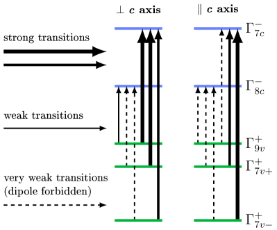
The energy levels of hex-Ge at the point are shown in Fig. 1. The CBM possesses symmetry. In agreement with group theory [27], optical dipole transitions from the three highest valence bands with symmetries , , and to the lowest conduction band are dipole forbidden except for the transition that is dipole allowed for light polarization perpendicular to the hexagonal axis [15]. However, its oscillator strength is three orders of magnitude smaller than the oscillator strength of typical dipole-active transitions in semiconductors [15]. Thus, hex-Ge can be called a pseudo-direct semiconductor that, despite having a direct band gap, is not optically active at the band-gap energy. However, there is a second conduction band with symmetry about above the CBM. Except for the transition for light polarization parallel to the axis, all transitions from the three highest valence bands to are (strongly) dipole active [27, 15].
In this work, we use accurate ab initio calculations to investigate if the ordering of the two lowest conduction bands can be inverted by applying moderate lattice strain to obtain a CBM with character and make hex-Ge an efficient light emitter. We also explore the possibility to tune the wavelength of light emission by strain [28]. A brief review of the used methods is given in Sec. II. The influence of strain on the atomic structure is studied in Sec. III. Section IV is dedicated to the analysis of strain effects on the electronic band structure. In Sec. V, we focus on the optical properties of strained hex-Ge. Finally, in Sec. VI, we present a summary and draw conclusions.
II Computational details
All calculations were performed in the framework of density-functional theory (DFT) as implemented in the Vienna Ab-initio Simulation Package (Vasp) [29, 30]. The wave functions are described using the projector-augmented wave method [31] with a plane-wave cutoff of . The Ge electrons are treated as valence electrons and spin-orbit coupling is included in all calculations. Unless otherwise noted, a -centered -point mesh is used for the BZ integration.
For the calculation of structural and elastic properties under strain, exchange and correlation are described in the generalized gradient approximation (GGA) using the PBEsol [32] functional. It has been previously shown that the PBEsol functional provides excellent lattice parameters for hexagonal Ge [15, 24]. The strained structures were optimized under constraint until the Hellmann-Feynman forces for all atomic coordinates were below . Symmetry-reducing strain on hexagonal nanowire facets is simulated in an orthorhombic supercell of the primitive hexagonal cell using a -point grid.
Electronic band structures were obtained with the meta-GGA functional MBJLDA, i.e. the modified Becke-Johnson exchange potential [33, 34, 35] together with the local-density approximation (LDA) for correlation. This meta-GGA functional yields excellent band gaps at low computational cost [14, 19, 15, 36], even though deviations from experiment or more sophisticated approaches (e.g. hybrid functionals or many-body perturbation theory) occur for electronic states further away from the band gap. Since we are mainly interested in the near-gap electronic structure here, this does not pose a problem for the present study. We carefully validated the choice of this functional for electronic-structure calculations of hex-Ge in Ref. [15].
Optical spectra and radiative lifetimes were calculated in the independent-particle approximation starting from the meta-GGA electronic band structure using a denser BZ sampling with -centered points.
III Structural and elastic properties
III.1 Equilibrium structure
The equilibrium geometry was obtained by constant-volume relaxation and a subsequent fit of the resulting energy-over-volume curve to the Birch-Murnaghan equation of state (EOS) [37]. For the lattice parameters of unstrained hex-Ge, we found , , and the internal cell parameter . Both and the ratio of are close to the values and of the ideal lonsdaleite structure. The lattice parameters are in very good agreement with available experimental data [24]. The EOS fit yields for the isothermal bulk modulus and for its pressure derivative.
III.2 Symmetry-conserving strain
For sufficiently small strains, the relation between the stress tensor and the strain tensor is linear, i.e. Hooke’s law
| (1) |
holds, with the tensor of elastic constants in Voigt notation [38] (). For hexagonal crystals, the symmetric elastic tensor has only five independent non-vanishing components [39, 40, 41]: , , , , , and .
First, we consider only normal stresses that leave the space-group symmetry unchanged. In this case, Hooke’s law reduces to
| (2a) | |||
| (2b) | |||
in hexagonal crystals, with the normal strains
| (3a) | |||
| (3b) | |||
that are given by the deviations of the strained lattice constants and from their equilibrium values and .
| Strain (PBEsol) | |||||||||||||||||
|---|---|---|---|---|---|---|---|---|---|---|---|---|---|---|---|---|---|
| Elastic (PBEsol) | |||||||||||||||||
| Ref. [42] | |||||||||||||||||
| Ref. [43] (LDA) | |||||||||||||||||
| Ref. [24] (exp.) |
III.2.1 Hydrostatic pressure
When a hydrostatic pressure is exerted on the system, the stress tensor reduces to . Inserting this constraint into Eq. (2) yields the relation between out-of-plane and in-plane strain, where is the hydrostatic ratio
| (4) |
The isothermal bulk modulus relates hydrostatic pressure to infinitesimal volume changes. For sufficiently small volume changes and pressures,
| (5) |
holds. Combining Eqs. (2), (4), and (5), the bulk modulus is given by
| (6) |
We simulate hex-Ge under hydrostatic pressure by a constrained relaxation of the atomic coordinates at a given fixed cell volume.
III.2.2 Biaxial strain
Biaxial strain perpendicular to the hexagonal axis is characterized by and , i.e. the forces along the axis vanish. Using Eq. (2), the out-of-plane strain can be linked to the in-plane strain by , where the biaxial ratio is given by
| (7) |
The in-plane stress is related to the in-plane strain as , with the biaxial modulus that reads
| (8) |
To model biaxial strain perpendicular to the axis in hex-Ge, the lattice constant is fixed and all other degrees of freedom of the atomic geometry are determined by total-energy minimization.
III.2.3 Uniaxial strain
For uniaxial strain along the axis, the in-plane normal stresses vanish and only is nonzero. Inserting this condition into Eq. (2) yields the relation between the in-plane and out-of-plane strains with the Poisson ratio
| (9) |
The uniaxial stress is related to the strain in this direction through the Young modulus
| (10) |
which follows immediately from Eq. (2).
Uniaxial strain can be modeled by fixing the lattice constant and relaxing all other atomic coordinates.
III.2.4 Elastic constants
For the situations of hydrostatic pressure, biaxial strain, and uniaxial strain, we determined the ratios between out-of-plane and in-plane strains for the smallest strains we investigated (about 1 %) and found , , and , respectively. Taking as additional input the bulk modulus from the EOS fit, the three elastic constants , , and , the biaxial modulus , and the Young modulus can be computed.
III.3 Symmetry-reducing strain
All elastic constants can be obtained by calculating normal and tangential stresses for specific deformations of the crystal lattice and solving Hooke’s law, as implemented in the code Elastic [44, 45]. The elastic constants obtained with Elastic confirm the values calculated for hex-Ge under hydrostatic pressure, biaxial strain, and unixaxial strain. A summary of structural parameters and elastic constants, including a comparison with results in literature, can be found in Table 1.
IV Electronic properties
IV.1 Symmetry-conserving strain
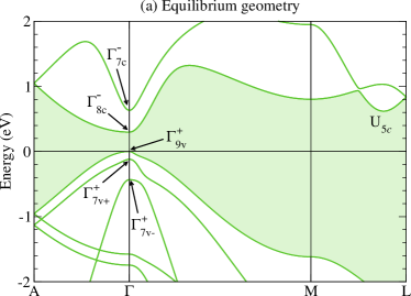
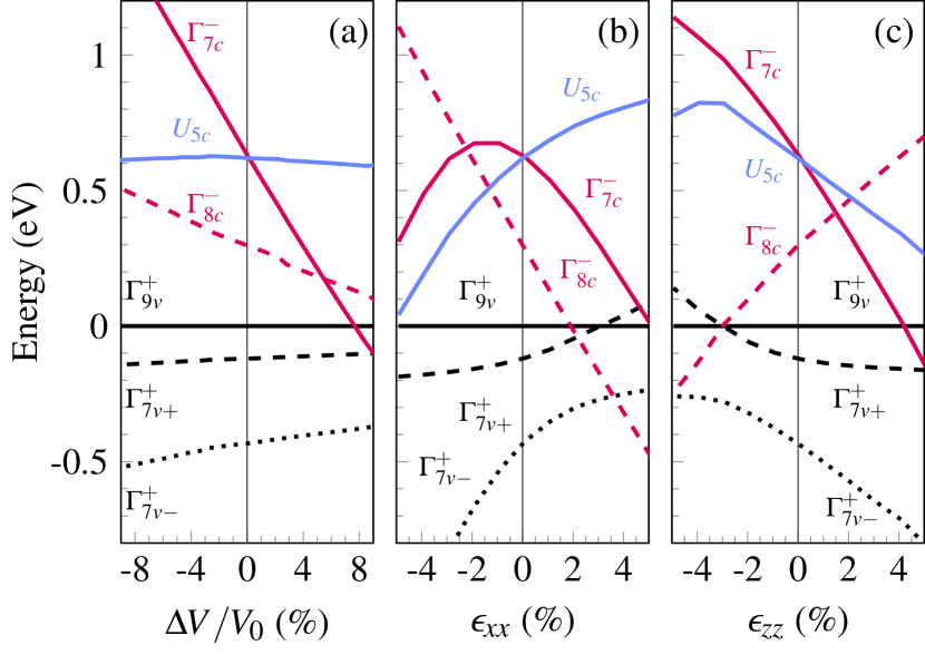
The band structure of unstrained hex-Ge is displayed in Fig. 2(a) along with the labels of relevant high-symmetry states [15]. Besides the energy levels at the point, the CBM is of particular interest, as it is close in energy to the CBMs at . Under some strains, the state on the - line becomes the lowest conduction level and turns hex-Ge into an indirect semiconductor which is, of course, not desirable for high light-emission efficiency, as this CBM would act as a carrier trap. The strain dependence of the band-edge energies is plotted in Fig. 3 for hydrostatic pressure, biaxial strain, and uniaxial strain. Here, the state, that is the valence-band maximum (VBM) for the unstrained structure, serves as reference level for all strain-induced energy shifts.
IV.1.1 Hydrostatic pressure
In general, we observe an increased splitting of all states at the point when hydrostatic pressure is exerted. Figure 3(a) shows that the VBMs at and the CBM shift only marginally in the investigated range of volume changes. However, the energy of the two CBMs at increases strongly with rising pressure. The effect is particularly pronounced for the state, as it forms an gap with the VBM [16].
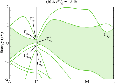
Negative hydrostatic pressure corresponding to a volume increase of about would lead to the desired conduction-band inversion of the and states with a pseudodirect-to-direct gap transition at a gap of . In Fig. 2(b), the band structure of hex-Ge for a volume dilatation of is shown, illustrating how the two CBMs approach. At even larger negative pressure, for volume increase, a semiconductor-to-metal phase transition occurs. Experimentally, negative hydrostatic pressures are hard, if not impossible, to realize, which is why this does not represent a promising route to engineer the electronic structure of hex-Ge. More sophisticated strains have to be explored.
IV.1.2 Biaxial strain
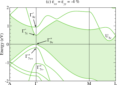
Figure 3(b) shows that the band ordering in hex-Ge is more sensitive to biaxial strain perpendicular to the hexagonal axis than to hydrostatic pressure. The state exhibits a highly nonlinear behavior leading to a conduction-band inversion for compressive biaxial strains larger than . Unfortunately, a direct-to-indirect-semiconductor transition with a fundamental gap occurs already at smaller compressive strains. The resulting band structure is illustrated in Fig. 2(c) for of compressive biaxial strain.
For tensile biaxial strain, the system becomes metallic at a strain of about . The band ordering resembles that of zincblende HgTe or -Sn [46] as a negative gap appears. Above of tensile strain, the band ordering changes to .
IV.1.3 Uniaxial strain
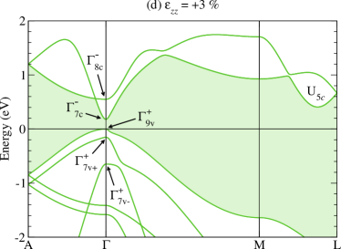
Uniaxial strain along the hexagonal axis offers great potential to engineer the electronic states, as the two CBMs and shift in opposite directions [see Fig. 3(c)]. Already for a small tensile uniaxial strains of about , a pseudodirect-to-direct gap transition occurs: hex-Ge becomes a direct-gap semiconductor with a gap of and strong dipole transitions at the gap energy. The gap stays direct, but shrinks for larger strains until a semiconductor-to-metal transition occurs at about tensile strain. Similar behavior has been observed experimentally for wz-GaAs [28] and wz-GaP [47] under uniaxial strain. The strain range between and is likely to be experimentally accessible and further offers the possibility to tune the band gap between 0 and . Figure 2(d) shows the band structure of hex-Ge for of tensile uniaxial strain illustrating the direct band gap and the band inversion at .
For tensile uniaxial strains above and compressive uniaxial strains above , we predict a band inversion of conduction and valence bands.
IV.1.4 Deformation potentials
| State | (eV) | (eV) | (eV) | (eV) |
|---|---|---|---|---|
In Table 2, the deformation potentials of the most important energy levels are compiled for the three considered symmetry-conserving strains. The deformation potentials are defined as the linear expansion coefficients of the energy levels as a function of strain,
| (11) |
with for hydrostatic pressure (), for biaxial strain (), and for uniaxial strain (). Note in particular that for biaxial and uniaxial strain, the strain dependence of the energy levels quickly becomes nonlinear. In these cases, the explicitly calculated values for the larger strains can be taken from Fig. 3.
The volume deformation potentials are very small for the states , , and . The potential of the gap is in excellent agreement with the value of for cubic Ge [48]. It is also close to the value of computed for wz-GaAs [49]. The volume deformation potential for the gap is significantly smaller. Also in this respect, hex-Ge behaves very similarly to wz-GaAs [49].
On average, the absolute values of the biaxial and uniaxial deformation potentials are larger than the volume deformation potentials, even when taking the relation for the strain amplitudes into account. For all studied states except , the biaxial and uniaxial deformation potentials have opposite sign. However, their absolute values differ, as tensile (compressive) biaxial strain and compressive (tensile) uniaxial strain do not represent the same physical situation.
IV.2 Symmetry-reducing strain
| Substrate | (Å) | (Å) | () | () |
|---|---|---|---|---|
| hex-Si | ||||
| wz-AlP | ||||
| wz-AlAs | ||||
| wz-GaP | ||||
| wz-GaAs | ||||
| wz-InP |
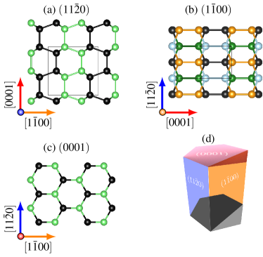
Pseudomorphic growth of hex-Ge on top of, e.g. wz-GaAs or wz-GaP substrates along the hexagonal axis does not permit to reach the preferential situation of tensile uniaxial strain. Growing instead on wz-GaAs or wz-GaP nanowire facets [23] represents a viable alternative to strain Ge along its hexagonal axis. However, the lattice mismatch between Ge and the nanowire substrate leads to a biaxial strain along the hexagonal axis and one of the or axes of the orthorhombic supercell shown in Fig. 4. The corresponding planes in the hexagonal cell are illustrated in Fig. 4, where also the top facet , i.e. the wire cross section, is indicated for comparison. Straining hex-Ge along the orthorhombic - ( plane) or - ( plane) facets reduces the space-group symmetry of hex-Ge which is why we refer to these strains as symmetry-reducing biaxial strains. For clarity, we use the same state labels as for the unstrained cells and the strained cells which conserve the full space group symmetry of the lonsdaleite structure.
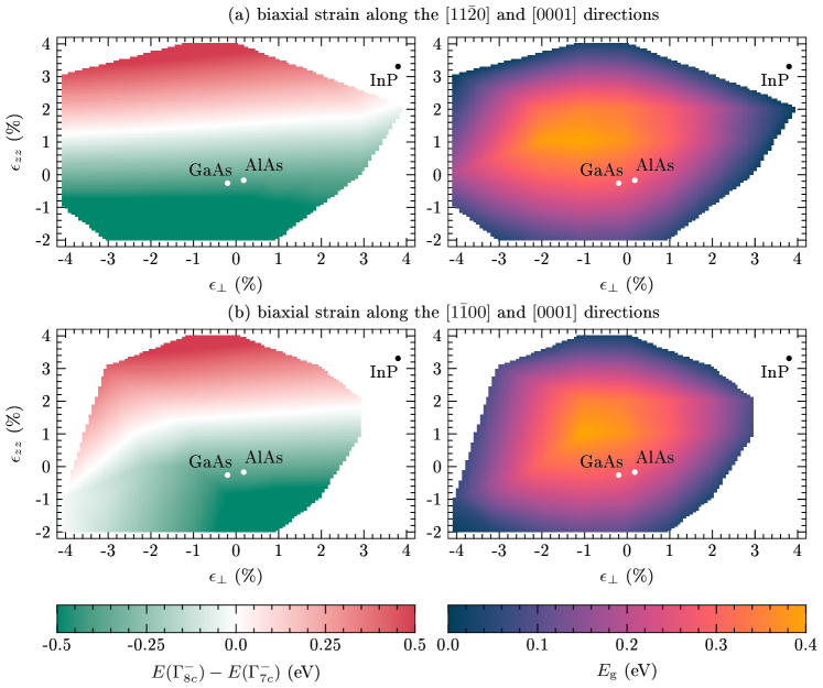
The energy difference between the two lowest conduction bands, and , as well as the size of the band gap at the point for symmetry-reducing biaxial strain are shown in Fig. 5. In view of laser applications, only strain configurations with a direct band gap are relevant, therefore only those will be discussed here.
The conduction-band ordering for biaxial strain along the facet is largely dominated by the strain component . The strain along the direction has almost no impact. Consequently, the general picture is very similar to uniaxial strain. A tensile strain of – yields the desired conduction-band inversion. Further increasing the strain reduces the value of the band gap until the material becomes metallic.
For biaxial strain in the plane, the conduction-band ordering is also dominated by the strain in direction. The conduction-band inversion occurs for – . Also here, the band gap decreases with increasing strain. Only for compressive strains in the plane perpendicular to the axis, the component has an equally strong influence and the conduction-band inversion occurs for lower . However, in this region, the gap is already very small. Therefore, we can conclude that the desired band ordering, which can be obtained for uniaxial strain, is stable with regard to small additional strains perpendicular to the axis.
We also checked whether a particular substrate can lead to lattice strain in the interesting regime. Some wurtzite substrates and their lattice mismatch relative to hex-Ge are listed in Table 3, and the resulting strain of the most interesting substrates is indicated in Fig. 5. None of the considered substrates could induce the desired results, but one could use either wz-GaAs or wz-AlAs as a substrate to grow almost strain-free hex-Ge. Wz-InP (wz-GaP, hex-Si) can serve as substrate for tensile (compressive) strain in hex-Ge overlayers.
V Optical properties
Always in view of optoelectronic applications, we analyze how the pseudodirect-to-direct band-gap transition induced by tensile uniaxial strain affects the optical properties near the fundamental band edge.
We calculate the dielectric tensor components in the independent-particle approximation using the optical matrix elements of the momentum operator between conduction band and valence band at a given -point applying the longitudinal gauge [51]. The diagonal elements of the imaginary part of the dielectric tensor are given by
| (12) |
with the valence and conduction band energies and . The unit-cell volume is denoted by and is the -point weight. In the calculations, the functions are represented by Lorentzians with a width of 0.05 eV. Excitonic effects can be neglected here. The dielectric constant of Ge is large, resulting in strong screening of the electron-hole interaction. Consequently, the exciton binding energy of cubic Ge amounts to only few meV [52] and similar values can be expected for the hexagonal structure. What is more, the symmetries of the band-edge states, which crucially govern the low-energy absorption and emission properties of hexagonal Ge, are not affected by the inclusion of the electron-hole interaction.
The global effect of tensile uniaxial strain on optical properties is illustrated in Fig. 6, where we show the imaginary part of the frequency-dependent dielectric tensor components () and the temperature-dependent radiative lifetimes which are calculated as detailed in Ref. [15].
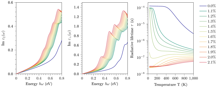
Unstrained hex-Ge does not exhibit an absorption peak at the fundamental band gap of . The first peak rather occurs at , the energy of the strong dipole transition between the highest valence band and the state. For increasing tensile uniaxial strain, this absorption peak shifts to lower energies, until it coincides with the band-gap energy for tensile uniaxial strains above as a consequence of the conduction-band inversion. For strains beyond the band-inversion point, the slope of the absorption edge is much steeper which is typical for a direct semiconductor with dipole-allowed transitions at the absorption edge. The analysis of the optical transition matrix elements at as a function of uniaxial strain along the -axis reveals an overall rather weak effect on the optical matrix elements. The smaller band gap for increasing strain induces a larger value of the imaginary dielectric function at the absorption edge, that is not compensated by the concomitant slight decrease of the optical matrix element of the transition.
The occurrence of band inversion for moderate uniaxial strain along the -axis is also obvious from the behaviour of the radiative lifetime. Tensile uniaxial strain above gives rise to drastic changes of the radiative lifetime. Below of strain, the lifetime curve shows the typical behavior of a system with two decay channels: a low-energy transition with small matrix element and a high-energy transition with large matrix element [15]. Upon increasing temperature, the impact of the high-energy transition becomes stronger and the lifetime drops by several orders of magnitude. The large low-temperature lifetime of is typical for a non-emitting system, the high-temperature value of rather corresponds to a direct semiconductor. For uniaxial strains above the pseudodirect-to-direct gap transition, the lifetime is of the order of – s and largely constant over the entire temperature range. This behaviour is characteristic for a system with one dominating decay channel as the band-edge transition in direct semiconductors [15] and shows that the strong dipole transition at the band gap outweighs all the rest.
The optical properties of uniaxially strained hex-Ge show that the material is an efficient light absorber with a dipole active direct-gap transition and low radiative lifetimes. Therefore, it is an interesting candidate material for silicon-technology based active optical devices which can compete with the light-emission efficiency of present-day III-V semiconductor devices.
VI Summary and conclusions
In summary, we have explored various possibilities to turn hexagonal Ge in the lonsdaleite phase with its pseudodirect band gap into a direct semiconductor with light-emission efficiencies suitable for technological applications. To this end, we investigated the impact of hydrostatic pressure, biaxial strain, and uniaxial strain on the electronic structure and the optical properties of hex-Ge. Hydrostatic pressure turns out unsuitable to obtain the desired modification of the conduction-band ordering and the concomitant pseudodirect-to-direct gap transition, as it occurs only for technically not accessible negative pressures. For biaxial strain within the hexagonal plane, either an insulator-to-metal transition occurs or the material becomes indirect before the conduction-band ordering changes.
For moderate tensile uniaxial strains between and , the desirable band inversion between the and conduction states is predicted by our calculations. The resulting gaps vary between and . Such strains are within reach of experimental realization. We could also show that small additional strain within the hexagonal plane, as it may occur in practical technological growth processes, has only little impact on the electronic structure. Uniaxially strained hex-Ge could, for instance, be pseudomorphically grown on the facets of III-V wurtzite-semiconductor nanowires.
The inversion of the two lowest conduction minima at makes hexagonal Ge an excellent absorber or emitter, with a radiative lifetime smaller by three order of magnitudes than the one of the unstrained material. Provided that a suitable growth method can be found, hex-Ge can be used as a direct light emitter compatible with CMOS technology. Another unexplored route that deserves future attention is the combination of strain with alloying of Ge and Si to control the size of the band gap and the conduction-band ordering at at the same time. This route is particularly promising considering that light emission form hexagonal SiGe nanowires has recently been demonstrated [24] and that the control of shape and strain of crystalline nanowires keeps showing great progress. [25]
Acknowledgements.
This work is supported by the European Commission in the framework of the H2020 FET Open project SiLAS (Grant agreement No. 735008). C. R. acknowledges financial support from the Marie Skłodowska-Curie Actions (Grant agreement No. 751823). Computing time was granted by the Leibniz Supercomputing Centre on SuperMUC (project No. pr62ja).References
- Miller [2009] D. A. B. Miller, Proc. IEEE 97, 1166 (2009).
- Srinivasan et al. [2014] S. Srinivasan, A. Arrighi, M. J. R. Heck, J. Hutchinson, E. Norberg, G. Fish, and J. E. Bowers, IEEE J. Sel. Top. Quantum Electron. 20, 8 (2014).
- Nam et al. [2014] D. Nam, D. S. Sukhdeo, S. Gupta, J. H. Kang, M. L. Brongersma, and K. C. Saraswat, IEEE J. Sel. Top. Quantum Electron. 20, 16 (2014).
- Geiger et al. [2015] R. Geiger, T. Zabel, and H. Sigg, Front. Mater. 2, 52 (2015).
- Joyce et al. [2011] H. J. Joyce, Q. Gao, H. Hoe Tan, C. Jagadish, Y. Kim, J. Zou, L. M. Smith, H. E. Jackson, J. M. Yarrison-Rice, P. Parkinson, and M. B. Johnston, Prog. Quantum Electron. 35, 23 (2011).
- Caroff et al. [2011] P. Caroff, J. Bolinsson, and J. Johansson, IEEE J. Sel. Top. Quantum Electron. 17, 829 (2011).
- Barrigón et al. [2019] E. Barrigón, M. Heurlin, Z. Bi, B. Monemar, and L. Samuelson, Chem. Rev. 119, 9170 (2019), pMID: 31385696.
- Galvão Tizei and Amato [2020] L. H. Galvão Tizei and M. Amato, Eur. Phys. J. B 93, 16 (2020).
- Zhang et al. [1999] Y. Zhang, Z. Iqbal, S. Vijayalakshmi, and H. Grebel, Appl. Phys. Lett. 75, 2758 (1999).
- Fontcuberta i Morral et al. [2007] A. Fontcuberta i Morral, J. Arbiol, J. Prades, A. Cirera, and J. Morante, Adv. Mater. 19, 1347 (2007).
- Hauge et al. [2015] H. I. T. Hauge, M. A. Verheijen, S. Conesa-Boj, T. Etzelstorfer, M. Watzinger, D. Kriegner, I. Zardo, C. Fasolato, F. Capitani, P. Postorino, S. Kölling, A. Li, S. Assali, J. Stangl, and E. P. A. M. Bakkers, Nano Lett. 15, 5855 (2015).
- Vincent et al. [2018] L. Vincent, D. Djomani, M. Fakfakh, C. Renard, B. Belier, D. Bouchier, and G. Patriarche, Nanotechnology 29, 125601 (2018).
- Rödl et al. [2015] C. Rödl, T. Sander, F. Bechstedt, J. Vidal, P. Olsson, S. Laribi, and J.-F. Guillemoles, Phys. Rev. B 92, 045207 (2015).
- Laubscher et al. [2015] M. Laubscher, S. Küfner, P. Kroll, and F. Bechstedt, J. Phys. Condens. Matter 27, 405302 (2015).
- Rödl et al. [2019] C. Rödl, J. Furthmüller, J. R. Suckert, V. Armuzza, F. Bechstedt, and S. Botti, Phys. Rev. Mater. 3, 034602 (2019).
- Raffy et al. [2002] C. Raffy, J. Furthmüller, and F. Bechstedt, Phys. Rev. B 66, 075201 (2002).
- De and Pryor [2014] A. De and C. E. Pryor, J. Phys. Condens. Matter 26, 045801 (2014).
- Kaewmaraya et al. [2017] T. Kaewmaraya, L. Vincent, and M. Amato, J. Phys. Chem. C 121, 5820 (2017).
- Chen et al. [2017] P.-S. Chen, S.-T. Fan, H.-S. Lan, and C. W. Liu, J. Phys. D 50, 015107 (2017).
- Vincent et al. [2014] L. Vincent, G. Patriarche, G. Hallais, C. Renard, C. Gardès, D. Troadec, and D. Bouchier, Nano Lett. 14, 4828 (2014).
- Zhang et al. [2000] Y. Zhang, Z. Iqbal, S. Vijayalakshmi, S. Qadri, and H. Grebel, Solid State Commun. 115, 657 (2000).
- Haberl et al. [2014] B. Haberl, M. Guthrie, B. D. Malone, J. S. Smith, S. V. Sinogeikin, M. L. Cohen, J. S. Williams, G. Shen, and J. E. Bradby, Phys. Rev. B 89, 144111 (2014).
- Hauge et al. [2017] H. I. T. Hauge, S. Conesa-Boj, M. A. Verheijen, S. Koelling, and E. P. A. M. Bakkers, Nano Lett. 17, 85 (2017).
- Fadaly et al. [2020] E. M. T. Fadaly, A. Dijkstra, J. R. Suckert, D. Ziss, M. A. J. v. Tilburg, C. Mao, Y. Ren, V. T. v. Lange, S. Kölling, M. A. Verheijen, D. Busse, C. Rödl, J. Furthmüller, F. Bechstedt, J. Stangl, J. J. Finley, S. Botti, J. E. M. Haverkort, and E. P. A. M. Bakkers, Nature 580, 205 (2020).
- Assali et al. [2019] S. Assali, M. Albani, R. Bergamaschini, M. A. Verheijen, A. Li, S. Kölling, L. Gagliano, E. P. Bakkers, and L. Miglio, Applied Physics Letters 115, 113102 (2019).
- Greenberg et al. [2019] Y. Greenberg, A. Kelrich, S. Cohen, S. Kar-Narayan, D. Ritter, and Y. Calahorra, Nanomaterials 9, 1327 (2019).
- Tronc et al. [1999] P. Tronc, Y. E. Kitaev, G. Wang, M. F. Limonov, A. G. Panfilov, and G. Neu, Phys. Status Solidi B 216, 599 (1999).
- Signorello et al. [2014] G. Signorello, E. Lörtscher, P. Khomyakov, S. Karg, D. Dheeraj, B. Gotsmann, H. Weman, and H. Riel, Nat. Commun. 5, 3655 (2014).
- Kresse and Furthmüller [1996] G. Kresse and J. Furthmüller, Comput. Mater. Sci. 6, 15 (1996).
- Kresse and Furthmüller [1996] G. Kresse and J. Furthmüller, Phys. Rev. B 54, 11169 (1996).
- Kresse and Joubert [1999] G. Kresse and D. Joubert, Phys. Rev. B 59, 1758 (1999).
- Perdew et al. [2008] J. P. Perdew, A. Ruzsinszky, G. I. Csonka, O. A. Vydrov, G. E. Scuseria, L. A. Constantin, X. Zhou, and K. Burke, Phys. Rev. Lett. 100, 136406 (2008).
- Becke and Johnson [2006] A. D. Becke and E. R. Johnson, J. Chem. Phys. 124, 221101 (2006).
- Tran et al. [2007] F. Tran, P. Blaha, and K. Schwarz, J. Phys. Condens. Matter 19, 196208 (2007).
- Tran and Blaha [2009] F. Tran and P. Blaha, Phys. Rev. Lett. 102, 226401 (2009).
- Borlido et al. [2019] P. Borlido, T. Aull, A. W. Huran, F. Tran, M. A. L. Marques, and S. Botti, J. Chem. Theory Comput. 15, 5069 (2019).
- Birch [1947] F. Birch, Phys. Rev. 71, 809 (1947).
- Voigt [1966] W. Voigt, Lehrbuch der Kristallphysik (Vieweg Teubner Verlag, 1966).
- Nye [1985] J. Nye, Physical Properties of Crystals: Their Representation by Tensors and Matrices, Oxford Science Publications (Clarendon Press, 1985).
- Wagner and Bechstedt [2002] J.-M. Wagner and F. Bechstedt, Phys. Rev. B 66, 115202 (2002).
- Hanada [2009] T. Hanada, “Basic properties of ZnO, GaN, and related materials,” in Oxide and Nitride Semiconductors: Processing, Properties, and Applications, edited by T. Yao and S.-K. Hong (Springer, Berlin, 2009) pp. 1–19.
- Fan et al. [2018] Q. Fan, C. Chai, Q. Wei, K. Wong, Y. Liu, and Y. Yang, J. Mater. Sci. 53, 2785 (2018).
- Wang and Ye [2003] S. Q. Wang and H. Q. Ye, J. Phys. Condens. Matter 15, 5307 (2003).
- Jochym and Badger [2018] P. T. Jochym and C. Badger, “jochym/elastic: Maintenance release,” (2018).
- Jochym et al. [1999] P. Jochym, K. Parlinski, and M. Sternik, Eur. Phys. J. B 10, 9 (1999).
- Küfner and Bechstedt [2015] S. Küfner and F. Bechstedt, Phys. Rev. B 91, 035311 (2015).
- Greil et al. [2016] J. Greil, S. Assali, Y. Isono, A. Belabbes, F. Bechstedt, F. O. Valega Mackenzie, A. Y. Silov, E. P. A. M. Bakkers, and J. E. M. Haverkort, Nano Lett. 16, 3703 (2016).
- Blacha et al. [1984] A. Blacha, H. Presting, and M. Cardona, Phys. Status Solidi B 126, 11 (1984).
- Cheiwchanchamnangij and Lambrecht [2011] T. Cheiwchanchamnangij and W. R. L. Lambrecht, Phys. Rev. B 84, 035203 (2011).
- Momma and Izumi [2011] K. Momma and F. Izumi, J. Appl. Crystallogr. 44, 1272 (2011).
- Gajdoš et al. [2006] M. Gajdoš, K. Hummer, G. Kresse, J. Furthmüller, and F. Bechstedt, Phys. Rev. B 73, 045112 (2006).
- Altarelli and Lipari [1976] M. Altarelli and N. O. Lipari, Phys. Rev. Lett. 36, 619 (1976).