2.5D Root of Trust: Secure System-Level Integration of Untrusted Chiplets
Abstract
Dedicated, after acceptance and publication, in memory of the late Vassos Soteriou. For the first time, we leverage the 2.5D interposer technology to establish system-level security in the face of hardware- and software-centric adversaries. More specifically, we integrate chiplets (i.e., third-party hard intellectual property of complex functionality, like microprocessors) using a security-enforcing interposer. Such hardware organization provides a robust 2.5D root of trust for trustworthy, yet powerful and flexible, computation systems. The security paradigms for our scheme, employed firmly by design and construction, are: 1) stringent physical separation of trusted from untrusted components, and 2) runtime monitoring. The system-level activities of all untrusted commodity chiplets are checked continuously against security policies via physically separated security features. Aside from the security promises, the good economics of outsourced supply chains are still maintained; the system vendor is free to procure chiplets from the open market, while only producing the interposer and assembling the 2.5D system oneself. We showcase our scheme using the Cortex-M0 core and the AHB-Lite bus by ARM, building a secure 64-core system with shared memories. We evaluate our scheme through hardware simulation, considering different threat scenarios. Finally, we devise a physical-design flow for 2.5D systems, based on commercial-grade design tools, to demonstrate and evaluate our 2.5D root of trust.
Index Terms:
Hardware Security, 2.5D Integration, Active Interposer, Chiplets, Multi-Core System, Runtime Monitoring, Policies1 Introduction
Security for computation systems has focused traditionally on software aspects, and it is understood that related efforts have to remain ongoing. Nowadays, the hardware itself has also become susceptible to misuse. Due to the economics of integrated circuit (IC) design and manufacturing, which dictates a production mode that is distributed across many vendors, an adversary involved at any step within the supply chain may, e.g., pirate the design intellectual property (IP) [1, 2]. Malicious modifications, also known as hardware Trojans, could also be introduced during design, manufacturing or deployment, and can be stealthy and severe, e.g., see [3]. Besides, even imprudent decisions made by legitimate designers can give rise to critical vulnerabilities, e.g., as demonstrated by the ZombieLoad attack [4]. These and other threats certainly impact the prospects for secure use of computation systems negatively.
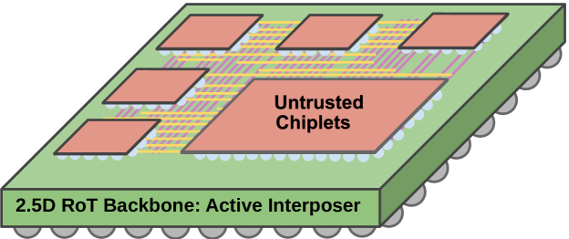
In this paper, we harness the opportunities offered by state-of-the-art 2.5D technologies for advancing hardware security. That is, we extend the scope for modern computation systems by means of a robust, system-wide, and hardware-enforced security scheme that is enabled by 2.5D design and construction (Fig. 1). Next, we discuss the background and motivation for our work in more detail.
1.1 Hardware Security Features
There exist many hardware security features (HWSFs), seeking to mitigate various software- and/or hardware-based threats at runtime. They include enclaves for trusted execution, like the industrial ARM TrustZone and Intel SGX or the academic MIT Sanctum (these and others are reviewed in [5]), wrappers for monitoring and cross-checking of untrusted third-party intellectual property (IP) modules [6], centralized IP infrastructures for secure system design [7], verification of computation [8], secure task scheduling [9], secure network-on-chip (NoC) architectures [10], etc. Besides, there are also design-time mitigation schemes, e.g., using high-level synthesis strategies for detection, collusion prevention, and isolation of malicious IP [11].
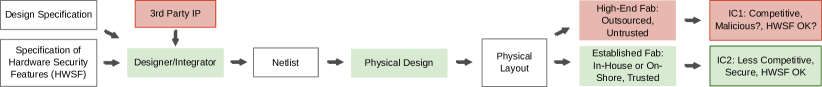
Notwithstanding their good prospects, most, if not all, HWSFs eventually suffer from tailored attacks, e.g., see [13] which exploits a memory corruption vulnerability in the enclave software of Intel SGX. In general, HWSFs arguably form prime targets—strategic adversaries would first aim to bypass or disable them so that further attacks can thereafter remain “under the radar.” Thus, HWSFs become especially vulnerable once adversaries can tamper with the outsourced IC supply chain (Fig. 2). (For other security concerns related to outsourced IC supply chains, see also, e.g., [2, 1, 11].) We note that the above circumstance also imposes an important practical challenge, namely how to implement ICs that are high-end, competitive, and relatively cheap, yet trustworthy and secure. This is because trusted manufacturing facilities (be they either in-house or on-shore and certified) typically cannot offer the latest high-end technology nodes, as doing so would be too costly.
To the best of our knowledge, none of the proposed HWSFs in prior art can fully withstand malicious modifications. Once HWSFs are permanently tampered with, even when such malicious activity is subsequently detected, the resulting loss of security guarantees cannot be restored—the chips become untrustworthy and as such possibly even unusable. We note that there are efforts to render hardware secure in the direct presence of Trojans; such schemes typically leverage some formalism like multi-party computation [14] or verification and proofing [8]. While promising, such schemes still require that at least some parts of the system remain trustworthy, i.e., that some parts are guaranteed to be free of any malicious modifications. Moreover, such schemes are less applicable to general-purpose, high-performance computation systems, as the underlying formalism requires extensive system- and circuit-level support, which naturally also tends to impose considerable overheads.
1.2 2.5D and 3D Integration
The umbrella of 2.5D and 3D integration technologies collectively embrace the notion of “building skyscrapers and city clusters of electronics” [15]. There exist two main drivers for 2.5D and 3D integration: 1) the CMOS scalability bottleneck, which becomes more exacerbated for advanced nodes by issues like routability, pitch scaling, and process variations; 2) the need to advance heterogeneous and system-level integration. Both drivers are also known as “More Moore” and “More than Moore,” respectively. Next, we provide a brief overview on the related technologies.
Native 3D integration means to vertically stack and interconnect multiple chips or active layers. This approach can be further classified by the underlying technology, with the main ones being: 1) through-silicon via (TSV)-based 3D ICs, 2) face-to-face (F2F) 3D ICs, 3) monolithic 3D (M3D) ICs [15]. Various studies, prototypes, and commercial products have shown that native 3D integration can indeed offer significant benefits over conventional 2D ICs, e.g., see [16, 17].
2.5D integration, also known as the interposer technology, facilitates system-level integration of 2D chips side-by-side. An interposer serves as an integration carrier and accommodates an underlying system-level interconnect fabric to provide inter-chip communication [18, 19, 20, 21], thereby resembling a modern version of a printed circuit board. Building an advanced electronic system using an interposer is considered less complex than native 3D integration [19, 18]. In fact, interposer-based systems are already established in the market, e.g., with the AMD Fiji GPU system [22] or Xilinx’s Virtex-7 FPGAs [23].
Besides classical passive interposer, comprising only passive components and wiring, a more promising option are active interposer which additionally incorporate logic. Active interposers have been successfully demonstrated, e.g., see [24, 20, 25]. Active interposers are preferably implemented using mature technology nodes, i.e., for commercial cost savings, yield, and, even more importantly for our work, ease of access to an established and trusted facility. Regarding manufacturing and integration cost, we note that both sides have been argued for, i.e., interposers are cheaper than 3D ICs [18] versus interposers are more costly [26]. However, once system-level cost are considered, the interposer technology remains promising, also because active interposers improve testability [24, 25, 20] and, thereby, allow to better manage yield of the final system.
Remarkably, the trend toward 2.5D and 3D integration can serve well to advance various notions of hardware security. Still, one has to account carefully for related limitations. For example, Valamehr et al. [27] propose a runtime monitor to be 3D-stacked on top of a commodity processor, along with dedicated HWSFs that allow for tapping and rerouting of sensitive signals. However, all these HWSFs rely on introspective interfaces within the commodity processor. Therefore, when subjected to an untrusted supply chain, that scheme could fail entirely once these interfaces in the commodity processor are tampered with. The authors themselves acknowledge this significant limitation in [27].
We provide a high-level overview on ours and selected prior works in Table I, and we discuss the motivation and contributions of our work in more detail in Sec. 1.4.
| Reference | Style | Security Scope; Means | Trusted Asset |
| [27] | TSV | Runtime monitoring; | Whole 3D IC |
| split manufacturing (SM) | |||
| [28] | 2.5D | IP protection; SM | Passive interposer |
| [29] | 2.5D | Trojan prevention; SM | Passive interposer |
| [30] | M3D | IP protection; camouflaging | Whole 3D IC |
| [31] | F2F | IP protection, Trojan prevention; | Only BEOL |
| SM, camouflaging | |||
| [32], | TSV | Side-channel mitigation; | Whole 3D IC |
| [33] | 3D integration by itself | ||
| Ours | 2.5D | Security by construction, | Active interposer |
| runtime monitoring; | |||
| stringent physical separation |
1.3 Chiplets: System-Level IP Integration
Concurrently, there exist efforts for driving the notion of IP reuse toward the system level. Under these efforts, not only IP modules are to be reused at the chip level, but rather entire chiplets at the system level. Chiplets are relatively small chips encapsulating certain levels of complex functionality, like a microprocessor, as hard physical IP. The potential benefits of using chiplets are lower design and manufacturing costs, improved yield through separating technologies, and greater design flexibility. As such, the economic benefits, especially for small-volume development of heterogeneous and large-scale systems, are becoming enormously promising. It is only logical that the 2.5D interposer technology is at the heart of these efforts.
A prominent initiative for chiplets integration is DARPA’s Common Heterogeneous Integration and Intellectual Property Reuse Strategies (CHIPS) [34]. The main objectives for CHIPS are: 1) realize a modular design process and manufacturing flow, and 2) establish standards for physical interfaces. Ultimately, the goal is to achieve “plug-and-play integration” of large-scale and heterogeneous systems, as opposed to the traditional, monolithic flow for 2D ICs. In general, chiplets integration has been well-received by both the academia (e.g., see [35, 19, 21]) and the industry, with relevant products and technologies already in the market, e.g., see the AMD Fiji system [22] and Intel’s Embedded Multi-Die Interconnect Bridge (EMIB) [36].
1.4 Motivation and Contributions
In this paper, we harness the opportunities offered by state-of-the-art 2.5D technologies for advancing hardware security. More specifically, we propose the assembly of: 1) potentially untrusted commodity chiplets and memories, and 2) physically separated, entrusted communication interfaces and HWSFs residing in an active interposer. We refer to the resulting system in general and the security-enforcing interposer in particular as 2.5D root of trust (RoT) (Fig. 1).
From a commercial point of view, we note that the system vendor has to design, produce, and sell such 2.5D RoT systems. Here, the good economics of chiplets reuse are still maintained; that vendor has to manufacture only a fraction of the overall system, namely the security-enforcing interposer (with the help of some established and trusted fabrication facilities) and would then integrate the high-end but untrusted chiplets on top of that interposer (with the help of in-house or certified on-shore packaging facilities). Therefore, the final system establishes security and can offer good performance at a reasonable cost—the crux illustrated in Fig. 2 can thus be resolved.
At this point, one might wonder about using a passive interposer for an alternative, potentially less costly implementation of an 2.5D RoT, but we argue that doing so would entail two key limitations. First, scalability would be compromised. This is because all HWSFs would have to be implemented within one or multiple, dedicated security chiplet(s), which would then become the “bottleneck” for system-level communication through the interposer. In fact, optimizing interposer interconnects is an area of research by itself, where active interposers are considered promising as well [37, 35]. Second, the need for trustworthy manufacturing of an interposer and some security chiplet(s) might well undermine the good economics of the scheme. In short, we advocate for an active interposer for our proposed 2.5D RoT.
This paper makes the following contributions:
-
•
We propose a novel 2.5D root of trust concept that, for the first time, establishes stringent physical separation at the system level, between 1) commodity chiplets and 2) HWSFs residing in an active interposer. In addition to ruling out common threat scenarios directly by construction, the purpose of this concept is to enable continuous runtime monitoring of the system-level communication of all commodity chiplets.
-
•
Following the 2.5D RoT concept, we showcase a secure multi-core architecture with a system-level interconnect fabric and shared memories. We implement our scheme using the Cortex-M0 core and the AHB-Lite bus system, both by ARM. We develop dedicated HWSFs for memory access and data control that form an integral part of our scheme. We release the license-free parts of our proof-of-concept (PoC) 64-core implementation to the community [38].
-
•
We develop an end-to-end physical-design flow for our 2.5D RoT, based on commercial tools. Our flow serves to design the active interposer and supports a flexible design mode for chiplets procured as soft or hard IP. Using this novel flow, we elaborate on the layout costs of our scheme in detail.
-
•
We evaluate our scheme against various relevant attack scenarios. We implement related security-enforcing policies and demonstrate them in action against malicious runtime behavior, using a commercial hardware simulation workflow.
2 Threat Model and Concept
Our concept does not require any trust assurance concerning the design and manufacturing of commodity chiplets. In fact, we even assume a priori that chiplets do run malicious code and/or incorporate Trojans.
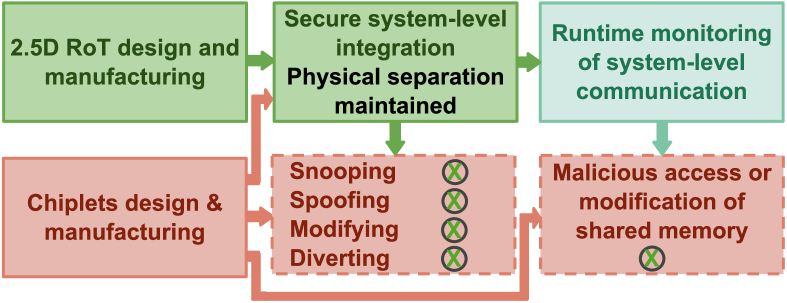
Crucially, such threats cannot undermine or compromise the system-level security of our scheme. This is due to the fact that our 2.5D RoT scheme imposes physically and inevitably that any untrusted component has to depend on the security-enforcing interposer for system-level communication, whereas the trustworthiness and robust operation of that interposer are not subject to those untrusted components. We note that this is in contrast to most prior art where HWSFs are embedded monolithically in the same chip and, thus, remain subject to the trustworthiness—or rather lack thereof—of all the related design and manufacturing stages.
Our threat model and concept are illustrated in Fig. 3, with details for both discussed next.
2.1 Security Threats and Assumptions
When seeking to securely integrate various components at the system level, different threats are to be considered, which concern the system-level communication and all involved components [6]. More specifically, in our work, a malicious chiplet may exercise the following attacks:
-
1.
Passive reading, also known as snooping, i.e., a chiplet illicitly reads or gathers data that is meant for/authorized to other chiplets;
-
2.
Masquerading, also known as spoofing, i.e., a chiplet disguises or poses itself as another one, to illicitly control services or request data from other chiplets;
-
3.
Modifying, i.e., a chiplet maliciously changes the data exchanged legally between other chiplets;
-
4.
Diverting, i.e., a chiplet maliciously diverts the data exchanged legally between two chiplets to a third, unauthorized chiplet; and/or
-
5.
Man-in-the-middle, i.e., a chiplet “hijacks” the communication between two chiplets—this attack is closely related to all four above.
As we focus on a multi-core architecture with shared memories, we also have to consider another threat:
-
6.
Malicious accesses and modifications of shared-memory-resident data.
We assume that any of these six threats can be introduced by: a) untrusted components/chiplets—either unintentionally via “design bugs” or intentionally via Trojans—or b) malicious software running on the cores.
We assume that any attack is exercised through system-level communication across chiplets. Therefore, any adversarial activities conducted within chiplets, such as covert channels across cores (e.g., [39]), side-channel- or fault-driven attacks across cores and their caches/buffers (e.g., [40, 4]), or fault injection on privileged hardware interfaces (e.g., [41]) are all considered out of scope for this work. Furthermore, we assume a trusted runtime environment. Thus, any threats like side-channel or physical fault-injection attacks conducted by malicious end-users (e.g., [42]) are considered out of scope as well.
Finally, we assume that the design and fabrication of commodity chiplets is outsourced and, hence, untrusted, whereas the design and manufacturing of the 2.5D RoT and the system-level assembly must all be carried out in a trusted environment. This also means that, in this work, we do not seek to detect or prevent Trojans within chiplets (recall that we rather assume a priori that Trojans are present in the untrusted chiplets). Given that related techniques (e.g., [43, 44]) are orthogonal to our efforts, such techniques could still be leveraged, to render the final system even more robust to begin with.
We note that, among other scenarios, DARPA’s CHIPS and DARPA’s Secure Processing Architecture by Design (SPADE) programs both match well with said assumptions. This is because government agencies seeking to build small numbers of large-scale, heterogeneous systems in a cost-efficient manner are advised to utilize chiplets which, when obtained from the open market, are potentially malicious. To ensure secure computation nevertheless, within a trusted runtime environment readily enforceable by the agencies, schemes like ours become essential.
2.2 Security Concept and Working Principles
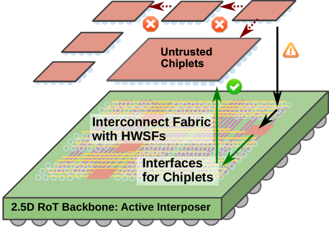
Our scheme is the first, to our best knowledge, that rules out the above threats 1)–5) by design and construction. As Fig. 4 illustrates, this kind of built-in security occurs as the system-level interconnect fabric with all its interfaces and HWSFs are physically separated from the untrusted components. Therefore, components/chiplets remain completely unaware of and isolated from any communication not directly addressed to or created by them. For example, regarding spoofing, we realize a hard-coded assignment of component identifiers (IDs) directly via the interconnect interfaces which are residing exclusively in the 2.5D RoT. Thus, a malicious component cannot masquerade itself as another in the first place.
Furthermore, we utilize the notion of security policies for runtime monitoring against malicious access or modification of the system-level shared memory. To do so, we devise HWSFs that allows us to enforce a fully-controlled memory access scheme. We apply stringent principles as follows, with related technical details provided in Sec. 3.
First, any memory access not explicitly allowed for, via some policy, is denied by default. Second, the continuous “policing” of memory access incurs uniform latency, independent of whether access is allowed or denied, and any denied access is responded to with a generic error message. These principles in conjunction ensure that an adversary cannot infer whether the requested region is protected or not used at all, which may serve well to hinder any related side-channel inference. Third, to protect against faults and malicious data modifications within memories themselves, we advocate for optional memory-security features like error correction codes (ECCs). Here, the actual data and the results of the security features are to be stored in physically separate locations and cross-checked upon reading.
In short, common threats are ruled out by construction, malicious memory accesses are blocked, and erroneous data is rejected; all these security principles are enabled directly at the 2.5D RoT. For any such adversarial case, the overall system may experience a (temporary) loss of functionality or data, but its integrity and trustworthiness remain intact, an outcome which constitutes the main focus of this work.
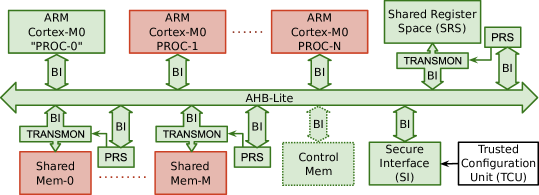
3 Architecture of 2.5D Root of Trust
Here we describe the architecture of our 2.5D RoT, called Interposer-based Security-Enforcing Architecture, or ISEA for short. The key paradigms of ISEA are: 1) to physically separate commodity components (chiplets in our case) from the HWSFs and 2) to monitor any memory-related, system-level communication at runtime. In more colloquial terms, one can memorize the term ISEA as “I see ya,” which reflects upon the idea of continuous system-level monitoring.
The novelty and enabler for ISEA is the security-enforcing active interposer, which serves as integration carrier and as “physical barrier” for any communication-centric security fallacies to propagate through the system. Toward that end, the interposer hosts the system-level interconnect fabric along with all proposed HWSFs. Therefore, any communication emanating from untrusted chiplets is inevitably handled and controlled by the interposer. More specifically, in this work, we focus on shared-memory transactions initiated by cores residing within chiplets. The legality of any such transaction is verified using various kinds of security policies; details and examples for such policies are provided further below and in Sec. 5.2.
3.1 System Implementation
3.1.1 Overview
Figure 5 depicts the block diagram for the proposed ISEA architecture. Key to ISEA are Transaction Monitors (TRANSMONs) which administer the various policies; the functionalities and implementation of TRANSMONs and all other HWSFs are explained in detail further below.
In this paper, without loss of generality, we consider the ARM Cortex-M0 core for the commodity chiplets. For the system-level interconnect fabric, we leverage the ARM Advanced High Performance Bus Lite (AHB-Lite). AHB-Lite facilitates communication among bus-attached master components (cores in our case) that initiate transactions and bus-attached slave components (system-level shared memories in our case) that respond to these requests. AHB-Lite transfers data values, addresses, and control info; it is managed by components such as arbiters, decoders, multiplexers, etc., all of which collectively implement the AMBA protocol (Advanced Microcontroller Bus Architecture). We choose AHB-Lite as it is technology-independent, widely used in the industry, and encourages modular design, all while offering high performance. Note that AMBA provides a secondary bus which functions as a slave to AHB-Lite, called the Advanced Peripheral Bus (APB), used for lower-bandwidth peripheral devices such as I/O ports. While APB could also be incorporated into ISEA, here we focus on AHB-Lite.
We release the license-free parts of our PoC implementation to the community [38]. We exhibit only a particular instance of ISEA here; our scheme can be easily retro-fitted to secure other systems, with different chiplets, cores, and/or interconnects. This is because the key principles of our scheme are agnostic to these implementation aspects.
We note that Cortex-M0 does not provide a cross-communication interface; hence, direct M0-to-M0 communication is not possible, thereby also excluding such direct message-passing for this PoC implementation of ISEA. Still, ISEA could be extended toward direct message-passing; TRANSMONs would be incorporated directly in-between the components to be monitored. This approach would also be applicable for, e.g., traditional system-on-chip (SoC) designs where IP cores may be connected via direct links. Besides, modern architectures may also contain hardware accelerators which can use integrated memories and/or external, shared memories. For the latter, the accelerators have to act as a bus master, like all other cores, to access those shared memories. Thus, ISEA can also be used to monitor transactions by other components, like accelerators, not just regular cores. Finally, ISEA could also be extended toward other types of system-level fabrics, like NoCs.
We emphasize again that it is essential for ISEA that the system-level interconnect fabric, its interfaces, and all proposed HWSFs are implemented exclusively in the active interposer, thereby constituting the 2.5D RoT by design and construction. For example, all communication requests passed onto the AHB-Lite bus system are associated with a master ID, whose assignment is handled by the bus-interface ports the chiplets are physically attached to—for ISEA, these ports are implemented in the trusted interposer, not within the chiplet. Thus, concerning spoofing, by construction there is no attack surface that could be leveraged by some Trojan or malicious software running within the chiplets and seeking to alter the master IDs. This and other scenarios are also illustrated in Fig. 10, Sec. 5.2.
3.1.2 Our Hardware Security Features
ISEA constitutes the following HWSFs:
-
1.
TRANSMONs, along with their Policy Register Spaces (PRSs) to store the various policies;
-
2.
a Shared Register Space (SRS);
-
3.
an ARM Cortex-M0 core called “PROC-0”; and
-
4.
the Secure Interface (SI).
The purpose of these features and their components is explained next.
1) A TRANSMON controls all transactions related to its attached memory chiplet, based on the policies stored in its PRS. A TRANSMON itself comprises three or four components: a) the Address Protection Unit (APU), b) the Data Protection Unit (DPU), c) the Slave Access Filter (SAF), and, optionally, d) a memory-security feature.
All components establish security collectively, with their functionality elaborated in Sec. 3.2. In a nutshell, the APU protects against undefined and/or unpermitted memory accesses, the DPU protects against illegal data modification or leakage of restricted data into the system’s shared memory space, the SAF serves to forward or reject requests which are approved or rejected, respectively, and the memory-security feature serves to detect faults and malicious modifications within the memories themselves.
2) The SRS can be used for secure data sharing, e.g., for semaphores. Although the SRS is implemented in the interposer, a TRANSMON and its related PRS are still required, to realize access control and runtime monitoring.
3) The interposer-embedded (and thus fully trustworthy) PROC-0 serves for scheduling and controlling the distributed computation, with commodity cores in the untrusted chiplets being allocated and interrupted by PROC-0 at runtime as needed. PROC-0 will further serve for mapping the system-level shared memory spaces, and for compiling and updating the application-specific sets of policies residing in the PRSs. It is important to note that PROC-0 does not constitute a “bottleneck” as it is not involved in each and every AHB-Lite transaction, but it is only used in exercising this kind of system-level management.
4) An external Trusted Configuration Unit (TCU) is responsible for loading the application(s) and initial data onto the system, and for retrieving the final results from the system. All these tasks are performed using the SI, which has privileged access to the AHB-Lite. Recall that we assume a trusted runtime environment; attacks misusing the TCU or SI in the field are thus out of scope. In any case, access to the TCU or SI can by protected by cryptographic primitives.
3.2 Transaction Monitor (TRANSMON)
Key to ISEA’s operation are TRANSMONs, with their micro-architecture illustrated in Fig. 6. Note that we choose to place an individual TRANSMON in-between every memory slave and the AHB-Lite bus interface (Fig. 5). While another option would be to place TRANSMONs in-between all the core masters and their respective bus interfaces, our design decision offers two important benefits. First, a TRANSMON connected to a master would require additional address bits decoding and checking (for the base address), which is already covered by AHB-Lite itself, whereas a TRANSMON connected to a slave only requires decoding and checking for the offset address. Second, a TRANSMON connected to a slave enables us to keep track of the security policies relevant to only that slave, thereby helping with efficiency.
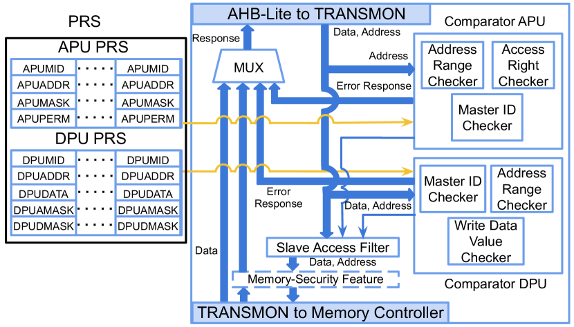
3.2.1 TRANSMON Design: Overview, Working Principles
As described, a TRANSMON comprises an APU, a DPU, an SAF, optionally a memory-security feature, and some glue logic. The APU and DPU each have access to their own PRS. For efficiency, every PRS is implemented using flip-flops. Each APU PRS entry defines one APU policy concerning some particular region in the system’s shared memory space, physically allocated in the memory slave connected to that TRANSMON; each DPU PRS entry defines one DPU policy concerning some particular data. Both APU and DPU policies are discussed in more detail below and examples are illustrated in Fig. 7 and Fig. 8.
TRANSMONs block all read or write requests that are violating any of their APU/DPU policies. By default, TRANSMONs also block requests that cannot be matched to any policy, protecting the system against all such “stray requests.” Policy verification also involves the checking of master/slave IDs. In this context, as we implement the interconnect fabric and all its interfaces physically exclusively in the active interposer, recall that there cannot, a priori, be any spoofing of IDs, snooping, modifying, or diverting of data, or man-in-the-middle attacks. In case a request is blocked, the related TRANSMON passes an error message to the master which initiated the transaction and an interrupt to the trusted PROC-0. The memory access itself is then dropped by the SAF—it is thus guaranteed to never reach the memory.
As indicated, the trusted PROC-0 within ISEA serves for mapping the system-level shared memory spaces, and for compiling and updating the application-specific sets of policies for each TRANSMON (more specifically, for its PRS). For different applications running on the system, depending on the scheduling, policies can also be devised for protection of independent data sets of multiple applications running in parallel. Once a particular application run is finalized, before dropping the related policies, PROC-0 should also clear the related memory regions, to avoid any posterior leakage of sensitive data. Moreover, the trusted end-user is free to implement software-level analysis and management of all blocked requests. Such management schemes may also decide whether masters which repetitively trigger requests to be blocked should be isolated completely from the system (by updating the policies accordingly), in order to mitigate potential denial-of-service attacks. In any case, software implementation for such “bootstrapping” and system-level management procedures are scope for future work; in this work, we focus on the ISEA architecture, the implementation and physical design of all its HWSFs, and on a security analysis based on functional hardware simulation runs.
3.2.2 TRANSMON Design: Address Protection Unit (APU)
The APU forms an integral part of the TRANSMON; it serves to check all read or write memory requests. As such, full access control over all shared-memory ranges is exercised. We design and implement the APU such that policy checking is acting during the address phase of the AHB-Lite protocol, thereby avoiding additional cycle delays.
Recall that each APU makes use of its own PRS to hold the polices related to its physically assigned memory slave. As Fig. 6 shows, an APU policy comprises four parameters:
-
•
APUMID, which identifies the master allowed to initiate the particular memory request described by this policy;
-
•
APUADDR, a 32-bit memory address;
-
•
APUMASK, a 32-bit address mask; and
-
•
APUPERM, the access permission, i.e., whether read-only, write-only, or read-write.
An example for an APU policy is illustrated in Fig. 7, and the related simulation is provided in Sec. 5.2.
3.2.3 TRANSMON Design: Data Protection Unit (DPU)
The DPU forms another integral part of the TRANSMON, and its function is to provide data-level protection. This is achieved by blocking: 1) over-writing of sensitive data in the event of unauthorized writes to specific memory locations, or 2) writing out particular data of sensitive nature. The latter serves to protect soft assets, e.g., private cryptographic keys, from leaking inadvertently into the system’s shared memory, e.g., by malicious “shadow writes” [6].
A write transaction is blocked when the DPU PRS contains a relevant policy that disables writing of particular, restricted data to a specified address range. Since DPU policy checks can only work during the data phase of the AHB-Lite protocol, we have to keep the data, address, and control signals all registered until the check is completed; this registering is done within the SAF. Hence, the DPU incurs one additional cycle delay in all transactions related to write-restricted data, but all other transactions not covered by DPU policies are not delayed.
As with the APU, recall that a DPU makes use of its own PRS. Figure 6 shows the five paramters of a DPU policy:
-
•
DPUMID, which identifies the master whose write transaction is to be verified against this policy;
-
•
DPUADDR, a 32-bit memory address, which designates the address where the write permission is restricted;
-
•
DPUDATA, a 32-bit, write-restricted data value;
-
•
DPUDMASK, a 32-bit data mask; and
-
•
DPUAMASK, a 32-bit address mask.
An example for a DPU policy is illustrated in Fig. 8, and the related simulation is provided in Sec. 5.2.
3.2.4 TRANSMON Design: Memory-Security Feature (Optional)
To protect against faults or malicious modifications within the shared system-level memories themselves, schemes like ECC, cyclic redundancy check (CRC), data mirroring, or a combination of these can be implemented. For example, an ECC implementation based on the well-known Hamming code would require four extra bits per memory byte, translating to 50% memory cost, and could only serve to detect at most two corrupted bits per byte. The advantage of ECC, however, is that it can be calculated during computation time without any latency overhead. A CRC implementation is more suitable when the memory data to protect is not supposed to change, e.g., for a firmware/software image. Also, CRC can be implemented with little additional circuitry. Still, the CRC computation needs to be run for chunks of data intermittently; this may halt some regular computation and can thus impact the overall throughput. In data mirroring, the data is simply copied into another (trusted) memory, which would naturally induce an overhead of 100%.
We envision some memory-security scheme as follows: 1) the TRANSMON computes an ECC for any write-out that is allowed; 2) the ECC result is stored in some separate and trusted control memory, whereas the actual data is stored in the shared-memory chiplet attached to the TRANSMON; 3) during read-out, the TRANSMON validates the data using the stored ECC result. If that check fails and cannot be corrected via the ECC, the data is rejected and the related memory region is marked as tainted and not used further.
Since address handling is covered by the AHB-Lite protocol, one may implement this scheme such that ECC results are fetched in parallel, without inducing additional delays for read-out transactions. We note that ECC results have to be stored in a trusted, separate memory chiplet. Finally, neither the above nor other memory-security features can protect against erroneous data arising from hardware/software failures or malicious activities. Such risks can only be mitigated at the system level, e.g., by redundant computation and majority voting on results [12, 45]. Note that a multi-core architecture like ours can be readily tailored for such needs, but related efforts are scope for future work.
4 Physical Design
Next, we elaborate on our end-to-end physical-design flow, which is devised for our 2.5D RoT, but can also be applied for any other active 2.5D system. The flow is illustrated in Fig. 9, and some highlights are discussed next. Note that the flow is leveraging commercial tools, libraries, and technologies for all key design steps such as placement and routing or handling of timing constraints; see also Sec. 5.1 for more details on the setup. For the interested reader/designer, we would also provide access to our flow upon request.
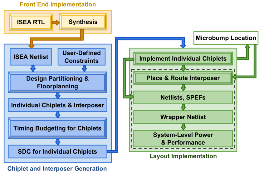
First, for the front-end implementation, the whole ISEA register-transfer level (RTL) design is synthesized to obtain a full-system netlist. Chiplets provided as soft IP are to be synthesized here as well.
4.1 Chiplets and Interposer Generation
The full-system netlist is then partitioned into banks, which simply represent the logic and memory chiplets. Our flow provides flexibility to the designer when choosing the number of logic/memory banks as needed for the chiplets organization. Based on the full-system netlist, we derive the timing budgets and obtain separate timing constraints (SDC files) for the individual chiplets and the active interposer.
Next, we generate the full-system floorplan. Relevant parameters are to be provided by the designer, such as utilization for individual chiplets and their aspect ratio, and they are used toward floorplanning of the related core/memory banks. Also, the floorplans of memory banks capture the placement of memory modules within each bank. The designer is also required to provide the arrangement of chiplets over the active interposer. Finally, the interposer die outline is derived from the full-system floorplan.
All the floorplan data is kept in Tool Command Language (TCL) format, which eases the use of a regular 2D implementation flow while designing the chiplets and the active interposer. We emphasize that our flow is flexible with respect to accommodating chiplets that are either designed in-house or, what is more practical, procured as physical hard IP from commercial vendors. For such hard IP, the design steps are more straightforward and essentially cover only the chiplets arrangement over the interposer and the design of the active interposer itself. When procuring such hard IP, it is easy to see that the designer has no freedom for any intra-chiplet optimization. Still, our flow allows the designer to explore different chiplet arrangements, which eases the system-level design space exploration along with an investigation of timing and power consumption.
4.2 Layout Implementation
For chiplets obtained as soft IP, the related netlists have to proceed through a standard 2D implementation flow, to obtain the individually placed-and-routed chiplet layouts. During this step, we also derive the locations for microbumps, which serve the physical connection between chiplets and the interposer. Those microbumps are initially placed around the vicinity of drivers/sinks, while further on-track legalization is performed to avoid routability issues and maximize the utilization of routing resources for the chiplets. Thereafter, the microbump locations of all chiplets are used to define the microbump locations for the interposer. Next, the RC parasitics for each chiplet are generated as SPEF files from their post-routed layouts. Along with the final netlist, these SPEF files are used later on for sign-off analysis, i.e., to evaluate power consumption and timing.
Once the 2D implementation of all chiplets is completed—which is skipped in case chiplets are obtained as hard IP—the placement and routing of the active interposer follow. First, the interposer netlist is imported, which describes the AHB-Lite components, the HWSFs of ISEA, and the pre-defined interposer microbump locations. Second, a 2D implementation of the active interposer follows. We note that we do not engage in any cross-optimization between chiplets and interposer, which is essential for the scenario of chiplets obtained as hard IP. Third, the RC parasitics for the active interposer design are extracted and exported along with the final netlist, and the GDSII is streamed out. Finally, the RC parasitics for the microbumps are modeled into the SPEF file of a wrapper netlist.
To evaluate the system-level power consumption and timing of ISEA, including all computing and memory chiplets, all individual netlists and their SPEF files are used along the wrapper netlist with its own SPEF file.
5 Experimental Evaluation
5.1 Setup
The RTL code for the complete system, including the cores, AHB-Lite bus, TRANSMONs, etc., has been realized using Verilog. We release the license-free parts of the RTL [38]. Synthesis was performed via Synopsys DC and layout generation via Cadence Innovus v.17.10. Verification and simulation runs have been carried out via Synopsys VCS. The ARM IAR suite has been used to compile C code to run on ISEA.
We implement ISEA as 64-core ARM Cortex-M0 multi-chiplet system for a PoC. As baseline, the 64 cores are organized into four computing chiplets, each holding 16 cores. For another configuration, to study the impact of system organization on layout costs, we reorganize the 64 cores into eight chiplets, each holding eight cores. Concerning security policies, our baseline configuration supports 16 APU and 16 DPU policies for each TRANSMON. To study the impact of policies being supported by TRANSMONs on layout costs, we also consider configurations with 32, 64, and 128 APU and DPU policies being supported by each TRANSMON.
For both the computing and shared-memory chiplets, we leverage the commercial 65nm GlobalFoundries technology and ARM standard cell and memory libraries, representing the advanced but untrusted facility. We employ four shared-memory chiplets with 1 MB SRAM each, build up from 16 memories at 64 kB. For the active interposer, we use the Synopsys SAED 90nm technology, representing the older but trusted facility. For brevity, we also refer to both technologies as 65nm and 90nm, respectively. Note that the 90nm technology does not provide memory modules; thus, we have to refrain from implementing any memory-security feature for this PoC, as we cannot provision for a separate, trusted memory chiplet required for such features. For both technologies, we use a supply voltage of 1.08 V, and we consider their respective slow corners. Note that doing so allows for heterogeneous 2.5D integration without the need for level shifters. In reality, the advanced but untrusted facility versus the older but trusted facility may support technology nodes that are further apart, but we were constrained in choices by the libraries available to us. Microbumps connecting the interposer and chiplets have a width of 5 and a pitch of 10. We utilize 7 metal layers for both the 90nm and the 65nm technology.
5.2 Security Analysis
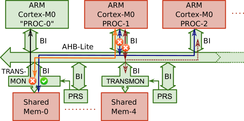
We study various scenarios for securing computation using ISEA. First, we illustrate how critical threats (i.e., snooping, spoofing, modifying, diverting, and man-in-the-middle attacks) are ruled out by ISEA in the first place (Fig. 10). More specifically, there is an approved transaction between PROC-2 and the shared memory with slave ID 0 (represented as blue arrow and green check in the TRANSMON of the memory). At the same time, PROC-1 seeks to snoop on that communication. This threat is blocked physically, directly by the BI (bus interface) of PROC-1, as the BI itself delegates only data originating from/destined to PROC-1. Next, PROC-1 tries to illicitly act as man-in-the-middle between PROC-2 and the shared memory with slave ID 4 (represented as dashed, dark-red arrow). This threat is blocked directly at the BI as well—the BI hard-codes the master ID 1 into any outgoing request, thereby preventing PROC-1 from masquerading its ID. Finally, PROC-1 also tries to access some data in the shared memory with slave ID 0 (orange arrow). However, this particular request is not approved by any policy and, thus, rejected. PROC-0 is informed about this blocked request as well (black arrow).
Next, we explore various scenarios for runtime monitoring against malicious access or modification of the system-level shared memory. These scenarios serve to show-case the working of ISEA in some detail, based on hardware simulation using Synopsys VCS along with C code compiled for the Cortex-M0 cores using ARM IAR. AHB-Lite signals relevant for understanding of these simulations are listed in Table II. Aside from the particular scenarios considered, the number of policies can increase and their interaction can become more complex in practice, depending on the application(s) running on ISEA and the resulting security requirements. We also note again that a full system-level software stack and related simulation efforts, also considering the orchestration and joint working of PROC-0 and the TCU, is scope for future work.
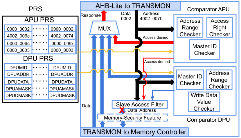
5.2.1 Protection of Memory Ranges
Here, ISEA is tasked exemplarily with executing a fast Fourier transformation (FFT). The FFT is an essential building block for many signal processing applications, and it can be parallelized straightforwardly. As indicated in Sec. 3, task scheduling is handled by the trusted control processor PROC-0, which also arranges the input data within the system’s shared memory space. The FFT computations within each core is started upon receiving an interrupt from PROC-0, and once the processing is done for all cores, the final results are gathered by PROC-0. Toward that end, we implement custom interrupt handler for the cores, to perform computation as controlled by PROC-0.
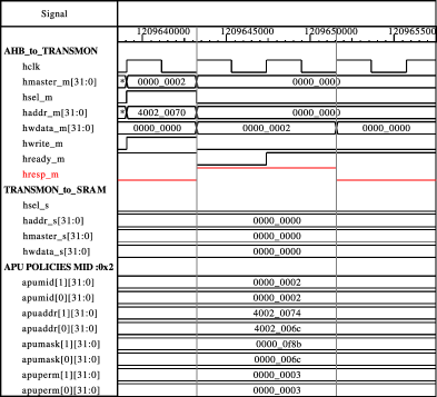
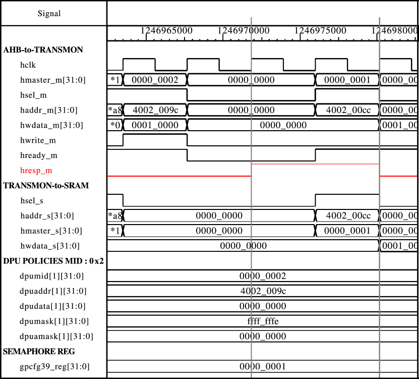
The policies are compiled such that the intermediate FFT results calculated by one core cannot be modified by other, maliciously acting cores. That is, we protect the shared-memory regions assigned to each core via APU policies. For example, the core with ID 0x2 has access to the address range 0x4002_0000 to 0x4002_006C and the range from 0x4002_0074 to 0x4002_0FFF, but not to other addresses such as 0x4002_0070 (i.e., where the core with ID 0x1 stores its result). Note that the address ranges are derived by the APU in an efficient manner, i.e., without need for complex comparator logic, using simple bit-wise operations. For example for the related simulation in Fig. 11(left), the start address 0x4002_0000 is APUADDR[1] AND NOT(APUMASK[1]) and the end address 0x4002_006C is APUADDR[1] OR APUMASK[1]; similarly, the start address 0x4002_0074 is APUADDR[2] AND NOT(APUMASK[2]) and the end address 0x4002_0FFF is APUADDR[2] OR APUMASK[2].
As shown in the waveform in Fig. 11(left), the core with ID 0x2 tries to access the address 0x4002_0070 to write out the data 0x0000_0002. Note that for AHB-Lite in general, the address phase comes first and the data phase one cycle after. The transaction is blocked by the APU, and the data in the memory remain protected and as is, indicated by the fact that the memory-controller signals are not reflecting the requested write out. At the same time, the error message hresp_m is returned. Finally, note that this particular example is the same as in the conceptional Fig. 7.
| Signal | Description |
|---|---|
| HCLK | Bus clock; timing of all signals is related to the rising edge of HCLK. |
| HMASTER | Master ID; a unique ID assigned to each master attached to the bus. |
| HSEL | Slave select; indicates that the current transaction is intended for the selected slave. |
| HADDR | System address; identifies the address as related to the slave. |
| HWDATA | Write data; used to transfer data from the master to the bus slaves during write operations and vice versa for read operations. |
| HWRITE | Transfer direction; HIGH indicates a write transfer, whereas LOW indicates a read transfer. |
| HREADY | Transfer status; HIGH indicates that a transfer has finished on the bus; to extend the transaction, this signal is to be driven LOW. |
| HRESP | Transfer response; provides feedback on the status of the transfer; used as receipt for security approval/rejection in our work. |
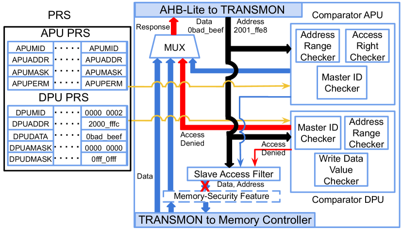
5.2.2 Protection of Private Assets
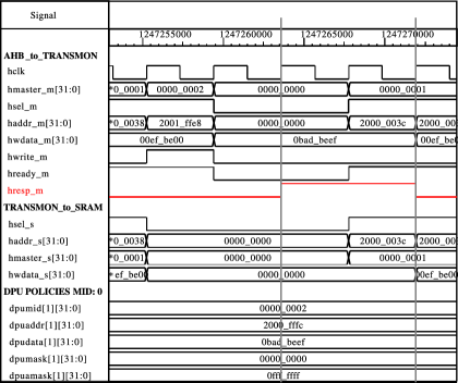
Here, a malicious core tries to write out some soft asset, e.g., a private cryptographic key. The DPU covers this kind of threat; the related DPU policy concerns the actual data.
For Fig. 11(right), a DPU policy is set to track a write transaction by the core with ID 0x2 to the restricted memory region between addresses 0x2000_0000 to 0x2FFF_FFFF, concerning the sensitive data 0x0BAD_BEEF. Note that the DPU derives address ranges like the APU; the start address is DPUADDR AND NOT(DPUAMASK) and the end address is DPUADDR OR DPUAMASK. Also, the sensitive data is derived similarly, as DPUDATA AND NOT(DPUMASK).
The simulation waveform in Fig. 11(right) shows an attempt to write out the restricted data value to address 0x2001_FFE8, which is blocked. Here as well, the error message hresp_m is returned. Note that subsequently another, unrelated read transaction is approved, which can be seen by the hready_m signal being turned on during the related data phase. Finally, note that this particular example is the same as in the conceptional Fig. 8.
5.2.3 Protection of Shared Assets
Here, we assume that two or more cores require a semaphore for software-based program and data control. Semaphores can be stored in the SRS, the shared register space, which is part of the 2.5D RoT, hence trustworthy by itself (Sec. 3). Consider a maliciously acting core tries to over-write the semaphore to be able to access/execute data/program regions otherwise not accessible. Here, a DPU policy is needed to monitor the actual data access to the semaphore, whereas a generic APU policy would not suffice.
Figure 12 shows how such a malicious transaction is blocked. Here gpcfg39_reg is considered as a semaphore register. For the core with ID 0x1, to obtain the ownership of this semaphore, it has to write 0x0000_0001 to the above register, but can do so only while the semaphore register value is 0x0000_0000, i.e., while the semaphore is available. For the core with ID 0x2, it has to write 0x0000_0010 to obtain the semaphore, and so on. Naturally, one core should not be able to obtain the semaphore when it is already used by any other core—a DPU policy is compiled to implement this restriction. In the simulation, the policy is set for the core with ID 0x02 to prevent any malicious writing of “0” to the last bit (DPUDATA AND NOT(DPUMASK)) of the semaphore register. The waveform shows such an attempt to clear that last bit, which is blocked, along with the error message hresp_m being returned. Note that the waveform shows subsequently another, unrelated read transaction initiated by the core with ID 0x01, which is approved.
5.3 Layout Analysis
Using our 2.5D design flow, we investigate the physical layouts of various ISEA configurations. In Fig. 13, we provide snapshots for the baseline 64-core 2.5D version of ISEA. We note that the details discussed below are based on our commercial-grade implementation setup (Sec. 5.1).
5.3.1 2D Implementation, ISEA in General
First, we analyze the impact of our security-enforcing features on layout costs. To do so, we compare the baseline ISEA multi-core design to a corresponding but non-secure design, both implemented via a regular 2D IC flow using the GlobalFoundries 65nm technology. For the non-secure design, we maintain all Cortex-M0 cores, memories, AHB-Lite components, and glue logic, but we drop all HWSFs such as TRANSMONs, PRSs, etc. We note that, from a conceptional point of view, using the Synopsys SAED 90nm technology would be more apt, as this technology was designated as the trusted node. Then, the corresponding secure 2D implementation would represent the system as implemented exclusively using the trusted technology. However, given that the 90nm technology does not provide memory modules, we have to resort to the 65nm technology. For this reason, we also refrain from directly comparing the secure 2D implementation with the secure 2.5D system later on.
Table III provides the results for the 2D implementation. For the secure design, we observe a 5% reduction in critical delay and a 13.86% increase in power consumption. Note that we achieve a competitive critical delay for the secure design by breaking longer paths using pipelining. An increase in standard-cell area (2.48%), instance count (29.57%), buffer count (18.46%), wirelength (31.49%), and total capacitance (35.44%) are all expected, due to the proposed HWSFs (including all registers required for storage of policies, etc.) and due to pipelining. The die outline remains as is, however; no additional silicon cost occurs. These results provide the range of costs to be expected for ISEA, that is at least for this particular PoC implementation.
| Metrics | Non-Secure (2D) | Secure (2D) |
|---|---|---|
| Critical Delay () | 9.79 | 9.29 |
| Power Consumption () | 239.5 | 272.7 |
| Standard-Cell Area () | 24,127,403 | 24,725,036 |
| Total Die Area () | 31,996,800 | 31,996,800 |
| Total Instance Count | 600,729 | 778,393 |
| Total Buffer Count | 132,477 | 156,929 |
| Total Wirelength () | 28.9 | 38.2 |
| Total Capacitance () | 7.9 | 10.7 |
5.3.2 2.5D Implementation
Table IV provides the physical-design results for the 2.5D baseline implementations. As indicated, computing and memory chiplets are implemented using the 65nm technology and the active interposer using the 90nm technology, respectively. Here we also compare a secure design with a non-secure design; both contain the same set of computing and memory chiplets, and both hold all AHB-Lite components in the active interposer, whereas the secure design further holds the proposed HWSFs in the interposer.
| Metrics | Non-Secure (2.5D) | Secure (2.5D) |
|---|---|---|
| Critical Delay () | 9.72 | 9.83 |
| Power Consumption () | 266.4 | 300.9 |
| Standard-Cell Area () | 24,588,292 | 26,844,473 |
| Total Die Area () | 33,641,866 | 33,641,866 |
| Interposer Die Area () | 6,237,600 | 6,237,600 |
| Total Instance Count | 569,574 | 745,693 |
| Interposer Instance Count | 69,742 | 249,085 |
| Total Buffer Count | 141,151 | 169,344 |
| Total Wirelength () | 30.5 | 40.5 |
| Total Capacitance () | 7.92 | 10.89 |
For the secure design, we observe an overhead of 1.13% for critical delay, 12.95% for power consumption, and 32.79% for wirelength, respectively. The standard-cell area is increased by 9.18%, while instance count and buffer counts are increased by 30.92% and 19.97%, respectively. As before, these costs are attributed to the HWSFs (including all PRS registers, etc.), but here the costs are further impacted by the migration to 2.5D and by the heterogeneous technology setup. More specifically, due to the migration to 2.5D, all the system-level interconnects are now passing through the active interposer, with all chiplets connected to this fabric through microbumps. Thus, timing closure for the interposer is subject to the multiple chiplets, which requires more effort. More importantly even, recall that the active interposer is implemented in the older 90nm technology. Therefore, higher costs are naturally to be expected, especially for all the HWSFs residing in the interposer. As with the 2D designs, there is no impact on the die areas for the 2.5D designs. In fact, the size of the interposer is dominated by the size and arrangement of the chiplets mounted on top of it, not by the standard-cell area of the additional logic incurred for the HWSFs within the interposer.
We emphasize again that we refrain from any cross-optimization between chiplets and the active interposer, to account for the practical assumption of hard-IP chiplets obtained as commodity components from the open market. Moreover, we note that our flow allows the designer to constrain the active area of the interposer (Fig. 13(right)) and the placement of microbumps (Fig. 13(left)). Doing so enables the final vendor to manufacture only a small CMOS chip for the interposer, instead of the whole outline, which naturally helps save commercial cost. Such a small chip could be supported by Intel’s EMIB technology [36].
We note that the results above are all subject to the ISEA PoC baseline configuration, i.e., 64 cores are organized into four computing chiplets, each holding 16 cores, and 16 APU and 16 DPU policies are supported by each TRANSMON. To understand the scaling of layout costs incurred by the proposed HWSFs, we next conduct the following experiments:
-
1.
We explore the impact for the number of policies being supported, by re-implementing the active interposer for 32, 64, and 128 APU and DPU policies being supported by each TRANSMON;
-
2.
We explore the impact of the system-level organization, by rearranging the 64 cores into eight computing chiplets with eight cores each and re-implementing the whole system.
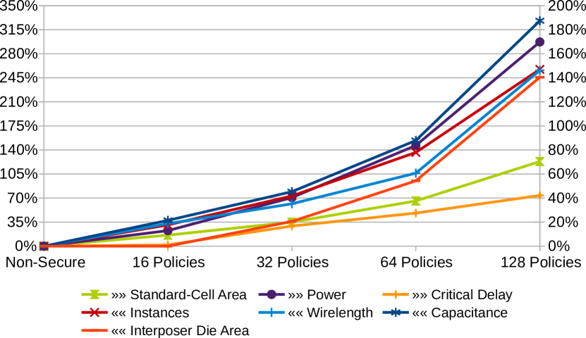
The results for 1) are illustrated in Fig. 14. We note that layout costs are scaling up as expected. More specifically, for each doubling of the number of policies being supported, most metrics are approximately doubled in cost as well (considering their respective baseline cost for the initial configuration supporting 16 policies). However, critical delays increase only linear—this indicates that the physical designs are well optimized in terms of performance/timing paths.
The results for 2) are as follows: the standard-cell area is increased by 0.99%, interposer die area by 47.35%, power by 2.13%, critical delay by -10.15% (i.e., reduced by 10.15%), total instance count is increased by 6.24%, total wirelength by 9.41%, and total capacitance by 6.24%, respectively. Given the reorganization of cores into double the number of computing chiplets, such costs are expected. More specifically, on the one hand, having to accomodate double the computing chiplets imposes a larger outline for the interposer. This is because the chiplets are not halved in size, as microbumps are dominating their outlines, and not the logic within. Due to the larger interposer die outline, we also observe larger total wirelength, along with more instances (required for buffering), higher capacitance, and marginally higher power consumption. On the other hand, the critical delay can be improved, thanks to some critical paths becoming shorter within the smaller computing chiplets, as well as due to the rearrangment of chiplets on top of the active interposer.
In short, these two experiments show reasonable costs, manifesting the practicality of our architecture for different configurations. We also like to argue that, for other systems beyond our Cortex-M0 PoC implementation, e.g., when using RISC-V cores instead, the layout costs might be better amortized over the respectively larger system.
Finally, we reiterate the fact that prior art is conceptionally different from ours. Prior art embedded their HWSFs monolithically within 2D ICs, whereas the risks related to adversaries in the IC supply chain have been largely overlooked. For the few studies considering HWSFs along with 2.5D/3D integration for protection at runtime (Table I), recall that their security promises are most often still subject to the design and manufacturing of the whole chip and the trust—or rather lack thereof—into the related facilities, e.g., as it is the self-declared case with [27]. Therefore, we argue that a comparative study of ours with prior art is neither meaningful nor practical and, hence, not provided here.
6 Conclusions and Future Work
We demonstrated a hardware security concept that provides a stringent physical separation, directly at the system level, between untrusted commodity components and trusted security-enforcing components. Our concept is in notable contrast to prior art where HWSFs are embedded monolithically in the same 2D IC as all other untrusted components and, thus, become inevitably subject to the trustworthiness of the design and manufacturing stages of that 2D IC.
For the first time, our architecture, dubbed ISEA, uses an active interposer as physically separate 2.5D root of trust, encompassing all proposed HWSFs and the system-level interconnect fabric. ISEA is based on stringent policy-based verification of every bus transaction, and serves to protect the system from various software- or hardware-emanating attacks. We provide the license-free parts of our proof-of-concept implementation, which is based on the Cortex-M0 core and the AHB-Lite bus system by ARM, in [38].
Our work establishes trustworthy computation in the face of untrusted commodity components integrated into a larger system, while maintaining the good economics of outsourced supply chains. In fact, the security-enforcing vendor only has to focus on the HWSFs and can integrate commodity chiplets as needed, while the system-level security remains intact even in the presence of any malicious behavior introduced by such chiplets. We believe that ISEA empowers secure computation by construction, while maintaining scalability and flexibility for various systems.
ISEA was tested at hardware simulation level under various threat scenarios and conceptionally demonstrated to offer robust security from malicious activities. Next, using our proposed, commercial-grade 2.5D physical-design flow, we explored the practical scenario of integrating hard-IP chiplets on an active interposer, with different technology nodes used for chiplets and the interposer.
For future work, we plan to extend ISEA for other system implementations, in particular with RISC-V cores. We also plan for system-level software implementation and simulation of ISEA, e.g., using gem5. We also plan to leverage our scheme for multi-party computation which, by definition, requires a root of trust for system-spanning security. Moreover, we plan to apply and study the notions of redundant computation and majority voting for critical applications.
In the longer term, we envision a holistic 2.5D root of trust, where we see the active interposer being augmented with side-channel sensors, e.g., to track power consumption of individual chiplets. As such, we would seek to track malicious activities which are more stealthy and refrain from targeting directly at system-level memory data.
Acknowledgments
This work was supported in part by the Center for Cyber Security at NYU New York/Abu Dhabi (NYU/NYUAD) and by the NYUAD REF scheme under grant RE218. The work of S. Patnaik was supported by the Global Ph.D. Fellowship at NYU/NYUAD.
References
- [1] S. Bhunia, S. Ray, and S. Sur-Kolay, Eds., Fundamentals of IP and SoC Security. Springer, 2017.
- [2] J. Knechtel, S. Patnaik, and O. Sinanoglu, “Protect your chip design intellectual property: An overview,” in Proc. Conf. Omni-Layer Intell. Sys., 2019, pp. 211–216.
- [3] K. Yang, M. Hicks, Q. Dong, T. Austin, and D. Sylvester, “A2: Analog malicious hardware,” in Proc. Symp. Sec. Priv., 2016, pp. 18–37.
- [4] M. Schwarz et al., “ZombieLoad: Cross-privilege-boundary data sampling,” in Proc. Comp. Comm. Sec., 2019, pp. 753–768.
- [5] P. Maene, J. Götzfried, R. de Clercq, T. Müller, F. Freiling, and I. Verbauwhede, “Hardware-based trusted computing architectures for isolation and attestation,” Trans. Comp., vol. 67, no. 3, pp. 361–374, 2018.
- [6] A. Basak, S. Bhunia, T. Tkacik, and S. Ray, “Security assurance for system-on-chip designs with untrusted IPs,” Trans. Inf. Forens. Sec., vol. 12, no. 7, pp. 1515–1528, 2017.
- [7] X. Wang, Y. Zheng, A. Basak, and S. Bhunia, “IIPS: Infrastructure IP for secure SoC design,” Trans. Comp., vol. 64, no. 8, pp. 2226–2238, 2015.
- [8] R. S. Wahby, M. Howald, S. Garg, and M. Walfish, “Verifiable ASICs,” Proc. Symp. Sec. Priv., pp. 759–778, 2016.
- [9] C. Liu, J. Rajendran, C. Yang, and R. Karri, “Shielding heterogeneous MPSoCs from untrustworthy 3PIPs through security-driven task scheduling,” Trans. Emerg. Top. Comp., vol. 2, no. 4, pp. 461–472, 2014.
- [10] L. Fiorin, G. Palermo, S. Lukovic, V. Catalano, and C. Silvano, “Secure memory accesses on networks-on-chip,” Trans. Comp., vol. 57, no. 9, pp. 1216–1229, 2008.
- [11] J. J. Rajendran, O. Sinanoglu, and R. Karri, “Building trustworthy systems using untrusted components: A high-level synthesis approach,” Trans. VLSI Syst., vol. 24, no. 9, pp. 2946–2959, 2016.
- [12] V. Mavroudis, A. Cerulli, P. Svenda, D. Cvrcek, D. Klinec, and G. Danezis, “A touch of evil: High-assurance cryptographic hardware from untrusted components,” in Proc. Comp. Comm. Sec., 2017, pp. 1583–1600.
- [13] J. Lee et al., “Hacking in darkness: Return-oriented programming against secure enclaves,” in Proc. USENIX Sec. Symp., 2017, pp. 523–539.
- [14] O. Bronchain, L. Dassy, S. Faust, and F.-X. Standaert, “Implementing Trojan-resilient hardware from (mostly) untrusted components designed by colluding manufacturers,” in Proc. Attacks Sol. Hardw. Secur., 2018, pp. 1–10.
- [15] J. Knechtel, O. Sinanoglu, I. A. M. Elfadel, J. Lienig, and C. C. N. Sze, “Large-scale 3D chips: Challenges and solutions for design automation, testing, and trustworthy integration,” Trans. Sys. LSI Des. Method., vol. 10, pp. 45–62, 2017.
- [16] M. M. Sabry Aly et al., “The N3XT approach to energy-efficient abundant-data computing,” Proc. IEEE, vol. 107, no. 1, pp. 19–48, 2019.
- [17] W. Gomes et al., “Lakefield and mobility compute: A 3D stacked 10nm and 22FFL hybrid processor system in 1212mm2, 1mm package-on-package,” in Proc. Int. Sol.-St. Circ. Conf., 2020, pp. 144–146.
- [18] J. H. Lau, “The most cost-effective integrator (TSV interposer) for 3D IC integration system-in-package (SiP),” in Proc. InterPACK, 2011.
- [19] D. Stow, Y. Xie, T. Siddiqua, and G. H. Loh, “Cost-effective design of scalable high-performance systems using active and passive interposers,” in Proc. Int. Conf. Comp.-Aided Des., 2017, pp. 728–735.
- [20] P. Vivet et al., “A 220GOPS 96-core processor with 6 chiplets 3D-stacked on an active interposer offering 0.6ns/mm latency, 3Tb/s/mm2 inter-chiplet interconnects and 156mW/mm2 @ 82%-peak-efficiency DC-DC converters,” in Proc. Int. Sol.-St. Circ. Conf., 2020, pp. 46–48.
- [21] J. Kim et al., “Architecture, chip, and package co-design flow for 2.5D IC design enabling heterogeneous IP reuse,” in Proc. Des. Autom. Conf., 2019, pp. 1–6.
- [22] C. C. Lee et al., “An overview of the development of a GPU with integrated HBM on silicon interposer,” in Proc. Elec. Compon. Tech. Conf., 2016.
- [23] P. Dorsey, “Xilinx stacked silicon interconnect technology delivers breakthrough FPGA capacity, bandwidth, and power efficiency,” Xilinc, Inc., Tech. Rep., 2010. [Online]. Available: https://www.xilinx.com/support/documentation/white_papers/wp380_Stacked_Silicon_Interconnect_Technology.pdf
- [24] S. Takaya et al., “A 100GB/s wide I/O with 4096b TSVs through an active silicon interposer with in-place waveform capturing,” in Proc. Int. Sol.-St. Circ. Conf., 2013, pp. 434–435.
- [25] G. Hellings et al., “Active-lite interposer for 2.5 & 3D integration,” in Proc. Symp. VLSI Circ., 2015, pp. T222–T223.
- [26] D. Velenis, M. Detalle, E. J. Marinissen, and E. Beyne, “Si interposer build-up options and impact on 3D system cost,” in Proc. 3D Sys. Integ. Conf., 2013, pp. 1–5.
- [27] J. Valamehr et al., “A 3-D split manufacturing approach to trustworthy system development,” Trans. Comp.-Aided Des. Integ. Circ. Sys., vol. 32, no. 4, pp. 611–615, 2013.
- [28] Y. Xie, C. Bao, and A. Srivastava, “Security-aware 2.5D integrated circuit design flow against hardware IP piracy,” Computer, vol. 50, no. 5, pp. 62–71, 2017.
- [29] F. Imeson, A. Emtenan, S. Garg, and M. V. Tripunitara, “Securing computer hardware using 3D integrated circuit (IC) technology and split manufacturing for obfuscation,” in Proc. USENIX Sec. Symp., 2013, pp. 495–510.
- [30] C. Yan, J. Dofe, S. Kontak, Q. Yu, and E. Salman, “Hardware-efficient logic camouflaging for monolithic 3D ICs,” Trans. Circ. Sys., vol. 65, no. 6, pp. 799–803, 2018.
- [31] S. Patnaik, M. Ashraf, O. Sinanoglu, and J. Knechtel, “A modern approach to IP protection and trojan prevention: Split manufacturing for 3D ICs and obfuscation of vertical interconnects,” Trans. Emerg. Top. Comp., vol. Early Access, 2019.
- [32] J. Knechtel and O. Sinanoglu, “On mitigation of side-channel attacks in 3D ICs: Decorrelating thermal patterns from power and activity,” in Proc. Des. Autom. Conf., 2017, pp. 12:1–12:6.
- [33] C. Bao and A. Srivastava, “Reducing timing side-channel information leakage using 3D integration,” Trans. Dependable Sec. Comp., vol. 16, no. 4, pp. 665–678, 2019.
- [34] D. S. Green. (2016) Common heterogeneous integration and IP reuse strategies (CHIPS). DARPA. [Online]. Available: https://www.darpa.mil/program/common-heterogeneous-integration-and-ip-reuse-strategies
- [35] J. Yin et al., “Modular routing design for chiplet-based systems,” in Proc. Int. Symp. Comp. Archit., 2018, pp. 726–738.
- [36] (2019, July) Intel unveils new tools in its advanced chip packaging toolbox. Intel. [Online]. Available: https://newsroom.intel.com/news/intel-unveils-new-tools-advanced-chip-packaging-toolbox/
- [37] I. Akgun, J. Zhan, Y. Wang, and Y. Xie, “Scalable memory fabric for silicon interposer-based multi-core systems,” in Proc. Int. Conf. Comp. Des., 2016, pp. 33–40.
- [38] (2020) The HDL framework for our 2.5D root of trust. DfX NYUAD. [Online]. Available: https://github.com/DfX-NYUAD/2.5D_ROT
- [39] R. J. Masti, D. Rai, A. Ranganathan, C. Müller, L. Thiele, and S. Capkun, “Thermal covert channels on multi-core platforms,” in Proc. USENIX Sec. Symp., 2015, pp. 865–880.
- [40] D. A. Osvik, A. Shamir, and E. Tromer, “Cache attacks and countermeasures: the case of AES,” in Cryptographers’ Track at the RSA Conference. Springer, 2006, pp. 1–20.
- [41] K. Murdock, D. Oswald, F. D. Garcia, J. Van Bulck, D. Gruss, and F. Piessens, “Plundervolt: Software-based fault injection attacks against Intel SGX,” in Proc. Symp. Sec. Priv., 2020.
- [42] E. Brier, C. Clavier, and F. Olivier, “Correlation power analysis with a leakage model,” Proc. Cryptogr. Hardw. Embed. Sys., vol. 3156, pp. 16–29, 2004.
- [43] Y. Lyu and P. Mishra, “Efficient test generation for Trojan detection using side channel analysis,” in Proc. Des. Autom. Test Europe, pp. 408–413.
- [44] R. S. Chakraborty, F. Wolff, S. Paul, C. Papachristou, and S. Bhunia, “MERO: A statistical approach for hardware Trojan detection,” in Proc. Cryptogr. Hardw. Embed. Sys., 2009, pp. 396–410.
- [45] A. Nguyen-Tuong, D. Evans, J. C. Knight, B. Cox, and J. W. Davidson, “Security through redundant data diversity,” in Proc. Int. Conf. Depend. Sys. Networks, 2008, pp. 187–196.
![[Uncaptioned image]](/html/2009.02412/assets/photos/nabeel.png) |
Mohammed Nabeel is a Chip Design Engineer from India. He received his Bachelors degree in electrical and electronics engineering from National Institute of Technology–Calicut, India. Mr. Nabeel is currently working as a Research Engineer at Center for Cyber Security at New York University Abu Dhabi (CCS-NYUAD). Apart from working on research in the field of hardware security, he also focuses on implementing and prototyping the research ideas in Chip. He has around 12 years of industry experience in chip design – specialized in Micro architecture, protocol know-how, RTL design, Synthesis, Static Timing Analysis and post silicon bring up. Prior to joining CCS-NYUAD, he worked at Texas Instruments, where he worked on chips targeted for IoT and Automotive and prior to that was with Qualcomm, where he worked on chips targeted for mobile phones and data cards. He has around 10 conference and journal papers and 1 issued US patent. |
![[Uncaptioned image]](/html/2009.02412/assets/photos/ashraf.jpg) |
Mohammed Ashraf received the bachelor’s degree in electronics and telecommunication engineering from the College of Engineering Trivandrum, Thiruvananthapuram, India, in 2005. He is a Senior Physical Design Engineer from India. He carries an experience of ten years in the VLSI industry. He has worked with various multinational companies like NVIDIA Graphics, Santa Clara, CA, USA, Advanced Micro Devices, Santa Clara, and Wipro Technologies, Bengaluru, India. He worked also with Dubai Circuit Design, Dubai Silicon Oasis, Dubai, United Arab Emirates. He is currently a Research Engineer with the Center for Cyber Security, New York University Abu Dhabi, United Arab Emirates. His work focus on the Physical Design/Implementation of the ARM Cortex M0 processor and its four secure variants. |
![[Uncaptioned image]](/html/2009.02412/assets/photos/satwik.jpg) |
Satwik Patnaik (Graduate Student Member, IEEE) received the B.E. degree in electronics and telecommunications from the University of Pune, India, and the M.Tech. degree in computer science and engineering with a specialization in VLSI design from the Indian Institute of Information Technology and Management, Gwalior, India. He is currently pursuing the Ph.D. degree with the Department of Electrical and Computer Engineering, Tandon School of Engineering, New York University, Brooklyn, NY, USA. He is also a Global Ph.D. Fellow with New York University Abu Dhabi, United Arab Emirates. His current research interests include hardware security, trust and reliability issues for CMOS and emerging devices with particular focus on low-power VLSI Design. Mr. Patnaik received the Bronze Medal in the Graduate Category at the ACM/SIGDA Student Research Competition held at ICCAD 2018, and the Best Paper Award at the Applied Research Competition held in Conjunction With Cyber Security Awareness Week, in 2017. |
![[Uncaptioned image]](/html/2009.02412/assets/photos/vassos.jpg) |
Vassos Soteriou (Senior Member, IEEE) received the B.S. and Ph.D. degrees in electrical engineering from Rice University, Houston, TX, in 2001, and Princeton University, Princeton, NJ, in 2006, respectively. He is currently an Associate Professor at the Department of Electrical Engineering, Computer Engineering and Informatics at the Cyprus University of Technology. He is a recipient of a Best Paper Award at the 2004 IEEE International Conference on Computer Design. His research interests lie in high-performance computing, multicore computer architectures, and on-chip networks. |
![[Uncaptioned image]](/html/2009.02412/assets/photos/sinanoglu.jpg) |
Ozgur Sinanoglu (Senior Member, IEEE) received the first B.S. degree in electrical and electronics engineering and the second B.S. degree in computer engineering from Boğaziçi University, Istanbul, Turkey, in 1999, and the M.S. and Ph.D. degrees in computer science and engineering from the University of California at San Diego, CA, USA, in 2001 and 2004, respectively. He is a Professor of electrical and computer engineering with New York University Abu Dhabi (NYU Abu Dhabi), United Arab Emirates. He has industry experience with TI, Dallas, TX, USA, IBM, Armonk, NY, USA, and Qualcomm, San Diego, CA, USA. He has been with NYU Abu Dhabi since 2010, where he is the Director of the Design-for-Excellence Lab. His recent research in hardware security and trust is being funded by U.S. National Science Foundation, U.S. Department of Defense, Semiconductor Research Corporation, Intel Corp, and Mubadala Technology. His research interests include design-for-test, design-for-security, and design-for-trust for VLSI circuits, where he has more than 180 conference and journal papers, and 20 issued and pending U.S. Patents. He has given more than a dozen tutorials on hardware security and trust in leading CAD and test conferences, such as DAC, DATE, ITC, VTS, ETS, ICCD, and ISQED. Prof. Sinanoglu won the IBM Ph.D. Fellowship Award Twice during his Ph.D. He is also the recipient of the Best Paper Awards at IEEE VLSI Test Symposium 2011 and the ACM Conference on Computer and Communication Security 2013. He was a (Guest) Associate Editor for the IEEE Transactions on Information Forensics and Security, the IEEE Transactions on Computer-Aided Design of Integrated Circuits and Systems, the ACM Journal on Emerging Technologies in Computing Systems, the IEEE Transactions on Emerging Topics in Computing, Microelectronics Journal (Elsevier), the Journal of Electronic Testing: Theory and Applications, and IET Computers and Digital Techniques journals. He is serving as the Track/Topic Chair or Technical Program Committee Member in about 15 conferences. |
![[Uncaptioned image]](/html/2009.02412/assets/photos/knechtel.jpg) |
Johann Knechtel (Member, IEEE) received the M.Sc. degree in Information Systems Engineering (Dipl.-Ing.) in 2010 and the Ph.D. degree in Computer Engineering (Dr.-Ing., summa cum laude) in 2014, both from TU Dresden, Germany. He is a Research Scientist with New York University Abu Dhabi, United Arab Emirates. From 2015 to 2016, he was a Postdoctoral Researcher with the Masdar Institute of Science and Technology, Abu Dhabi; from 2010 to 2014, he was a Ph.D. Scholar and Member with the DFG Graduate School on “Nano- and Biotechnologies for Packaging of Electronic Systems” hosted at TU Dresden; in 2012, he was a Research Assistant with the Chinese University of Hong Kong, Hong Kong; and in 2010, he was a Visiting Research Student with the University of Michigan at Ann Arbor, MI, USA. His research interests cover VLSI physical design automation, with particular focus on emerging technologies and hardware security. He has (co-)authored around 50 publications. |