Coulomb blockade thermometry beyond the universal regime
Abstract
The charge localization of single electrons on mesoscopic metallic islands leads to a suppression of the electrical current, known as the Coulomb blockade. When this correction is small, it enables primary electron thermometry, as it was first demonstrated by Pekola et al. (Phys. Rev. Letters, 73, 2903 [1994]). However, in the low temperature limit, random charge offsets influence the conductance and limit the universal behavior of a single metallic island. In this work, we numerically investigate the conductance of a junction array, and demonstrate the extension of the primary regime for large arrays, even when the variations in the device parameters are taken into account. We find that our simulations agree well with measured conductance traces in the submillikelvin electron temperature regime.
I Introduction
Single electron charging effects are prominent in isolated nanoscale conductors below a characteristic temperature scale [1, 2], where is the Boltzmann constant, is the electron charge and is the total capacitance of the metallic island. In this low temperature regime, charge sensing [3] and direct current measurements through tunneling contacts with low conductance, [4] yield a well-defined number of excess electrons on small metallic islands and an exponentially suppressed tunneling current. Increasing the temperature to results in the breakdown of Coulomb blockade, and it was shown that in this regime, the conductance suppression is universal. This enables a primary measurement of the electron temperature [5], which is insensitive to the device geometry, the external magnetic field [6] and the electrostatic environment of the device [7]. This property makes Coulomb blockade thermometry favorable for metrological applications [8, 9, 10, 11], and several experiments were performed in cryogenic temperatures ranging down to the millikelvin [12, 13, 14, 15, 16, 17, 18] and submillikelvin regime [19] as well as up to K [20].
The practical upper temperature range of a Coulomb blockade thermometer (CBT) is limited by the readout of the low bias conductance suppression, which is inversely proportional to the temperature [10, 20]. In the low temperature limit, the conductance depends on the electrostatic environment of the device, which imposes an effective offset charge [4, 21]. This offset charge depends on the random, uncontrolled population of charge traps at nearby interfaces and charged impurities inside dielectrics [22, 23] leading to a statistical error for primary electron thermometry by CBTs.
Precision electron thermometry requires a characterization of this error source. In particular, the recent advent of ultralow-temperature quantum electronics [24, 25, 26] requires electron thermometry spanning several orders of magnitude in temperature. Here, we use a statistical Monte Carlo approach to investigate the temperature error sources of CBTs in the low temperature regime, and demonstrate that this numerical procedure provides a unified description of a CBT, matching the predictions of the commonly used single island master equation (ME) model [5] in the high temperature, universal regime. Importantly for Coulomb blockade thermometry, we show that the effect of random offset charges is suppressed in the case of large arrays, which enables reliable temperature measurements deeper in the low temperature regime, even in the presence of variations in the device parameters. Finally, we demonstrate the applicability of our numerical results by a direct comparison with ultralow-temperature experimental data, where previous numerical and analytical models fail to describe the conductance of the CBT.
II Electrostatics of the CBT device

We consider the device geometry outlined in Fig. 1, which displays the typical implementation of a CBT consisting of tunnel junctions in series enclosing islands. Each junction possesses a resistance and a parallel capacitance . Crucially for the current work, we also consider the offset-charge of each island, yielding a total charge , where the number of excess electrons on the island is . Throughout this work, we assume that the effective gating capacitance is much smaller than and for all islands and investigate the applicability of this limit for experiments in Section 7.
The array is symmetrically biased by two voltage sources, fixing the electrostatic potential on the leftmost and rightmost nodes at and respectively, leading to a total voltage drop of . We neglect environment-assisted tunneling processes [27] assuming a low-impedance electromagnetic environment surrounding the device.
In our analytical and numerical calculations, we always consider a single series of junctions first and sum up the resulting conductances to model arrays. This method is equivalent to neglecting the capacitive coupling between islands in neighboring chains, which is justified in typical device geometries.
We now consider the electrostatic potential of each island for , which allows us to express the total charge on the island:
| (1) |
where and . We can write this equation in a matrix form, with
| (2) |
where , the total capacitance of island .
Finally, the electrostatic potentials define the voltage drop over each tunnel junction as and the total electrostatic energy is given by
| (3) |
We now consider a homogeneous array in the absence of offset charge, where all and , at zero bias voltage, . In this limit, the electrostatic energy of a single electron on island is calculated using the net capacitance , which yields
| (4) |
Substituting and or , Eq. (4) yields the charging energy expression
| (5) |
which defines the dimensionless inverted temperature [5, 28].
Turning to the effect of a finite offset charge on all islands of a homogeneous array, we derive the condition where the change of (see Eq. (3)) is zero in response to a single electron tunneling event (isoenergetic tunneling). With zero excess electrons on all islands, charge conservation yields the following expression for the voltage drops over the tunnel junctions:
| (6) |
and . If we now insert a single excess electron onto island , holds with the other differences remaining the same. We can now zero out with the following index shift:
| (7) |
which is fulfilled for any when , yielding independent of the bias voltage .
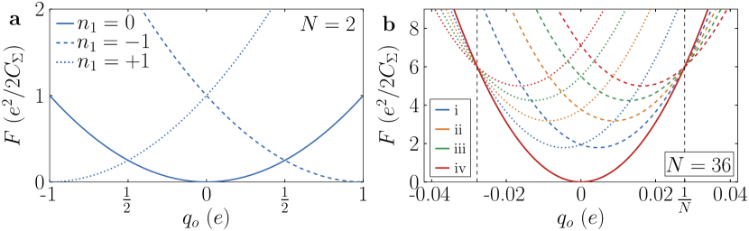
This result has important consequences to the charge degeneracy of the device. The well-known charge degeneracy condition of in case of a single island changes to for an array of tunnel junctions, where the total electrostatic energy of an empty chain is equal to the energy when a single excess electron is present on any of the islands. We illustrate this effect by plotting at as a function of in the case of and excess charge in the case of (Fig. 2a) and (Fig. 2b), where different positions of the excess charge are shown, all intersecting at . This result shows that in the low temperature regime, we should expect the highest conductance of a CBT array at this offset charge corresponding to minimal Coulomb blockade [29].
III Numerical model
We now introduce the numerical method leading to the voltage-dependent differential conductance of a CBT array at an arbitrary temperature. We base our calculations on the Markov chain Monte Carlo (MCMC) method [30, 31], which allows us to investigate arbitrary array sizes, offset-charge configurations, and variations in the parameters of the tunnel junctions.
Here the system is described by a chain of randomly selected single charge tunneling events altering to , which is written in a matrix form for :
| (8) |
The first (last) columns describe the forward (backward) tunneling of one charge quantum. Next we evaluate the resulting potentials in a concise form and calculate the associated free energy change for a single electron hopping through junction [30]:
| (9) |
Here, and at a bias voltage (Fig. 1b). We note that for a homogeneous array with , the above expressions lead to , which was also used to find the analytic high temperature curve for the case [5]. Based on , we calculate the forward and backward tunneling rates through junction with a resistance :
| (10) |
The tunneling current is a result of the single charge tunneling events. Following standard Monte Carlo methods, we consider the current charge configuration and evaluate the corresponding values. Then, we randomly select the realized tunneling process with a probability proportional to the corresponding tunneling rate. In addition, we follow the variance reduction method introduced by [31, 32] to calculate . Here, we make use of the current conservation along the tunnel junction chain, and express the total current as using [32]:
| (11) |
| (12) |
where the Monte Carlo step runs in the range of , which we set to reach a relative error less than , typically achieved with . We numerically acquire the differential conductance as , where . Finally, we recover the asymptotic tunnel conductance at high bias voltages as .
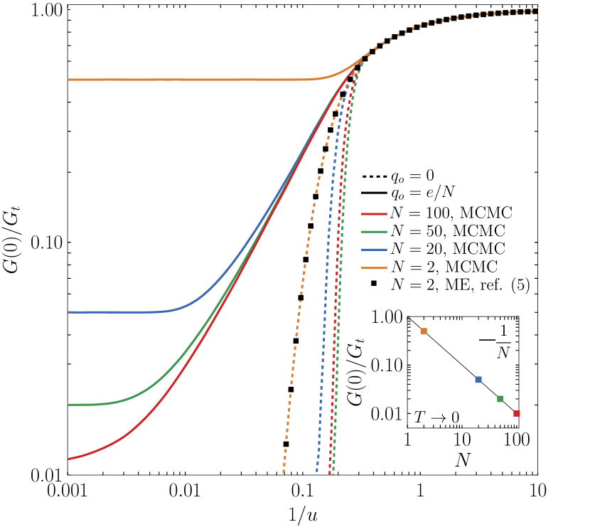
First, we discuss the dimensionless zero bias conductance , which we plot in Fig. 3 for various values and for the two limiting cases in homogeneous offset charge, (dashed lines) and (solid lines). We benchmark our numerical MCMC results in the well-studied high temperature regime, where . Here, we recover the earlier results [5, 29] that the conductance collapses onto a single curve independent of and . The conductance in this limit has been calculated earlier by writing a master equation for forward and backward tunneling processes for a single island device with . Here, the conductance suppression follows a series expansion in [5, 29]:
| (13) |
In the low temperature limit, we find that the conductance depends on , and the case corresponding to strong Coulomb blockade results in an exponential suppression of the conductance. However, at minimal blockade, , our results yield a low temperature saturation conductance corresponding to (see inset of Fig. 3), which is the extension of the case discussed earlier [29].
We understand this result based on the charging energy expression summarized in Fig. 2, where all possible states with a single excess electron and the empty chain have the same electrostatic energy if . Since all other charge configurations are higher in energy, only these states are occupied at zero temperature, with an equal probability of . Taking the limit of Eq. (10), we find
| (14) |
if (forward tunneling) and otherwise. We calculate the current as through any of the tunnel junctions. At low bias, where , we get , which yields . With and , we arrive to the dimensionless conductance
| (15) |
corresponding to the numerically acquired result. This conductance and its exponentially suppressed counterpart at demonstrates the increasing sensitivity of a CBT to the offset charge as the temperature is lowered below . Furthermore, in this regime, the commonly used analytical master equation model with fails to predict regardless of , underlining the importance of MCMC numerics for low temperature Coulomb blockade thermometry.
Next, we perform the analysis of the finite bias curves, which is commonly used for primary calibration in the universal regime. Here, the full width at half minimum [5, 28]
| (16) |
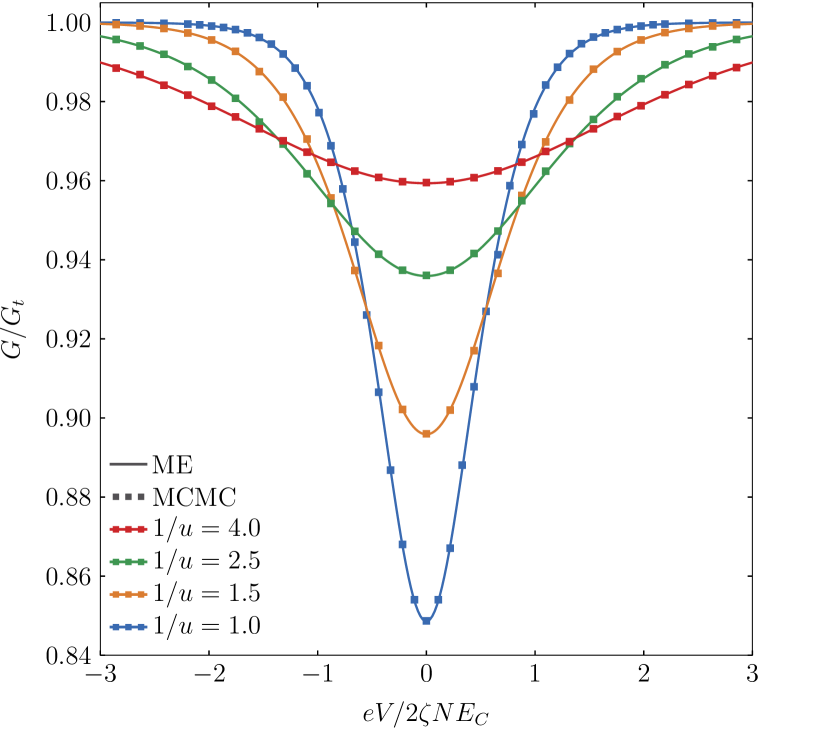
with enables primary thermometry if or the characterization of for secondary thermometry with using Eq. (13). We first demonstrate that MCMC calculations reproduce the master equation conductance traces in the universal regime and yield the same (Fig. 4).
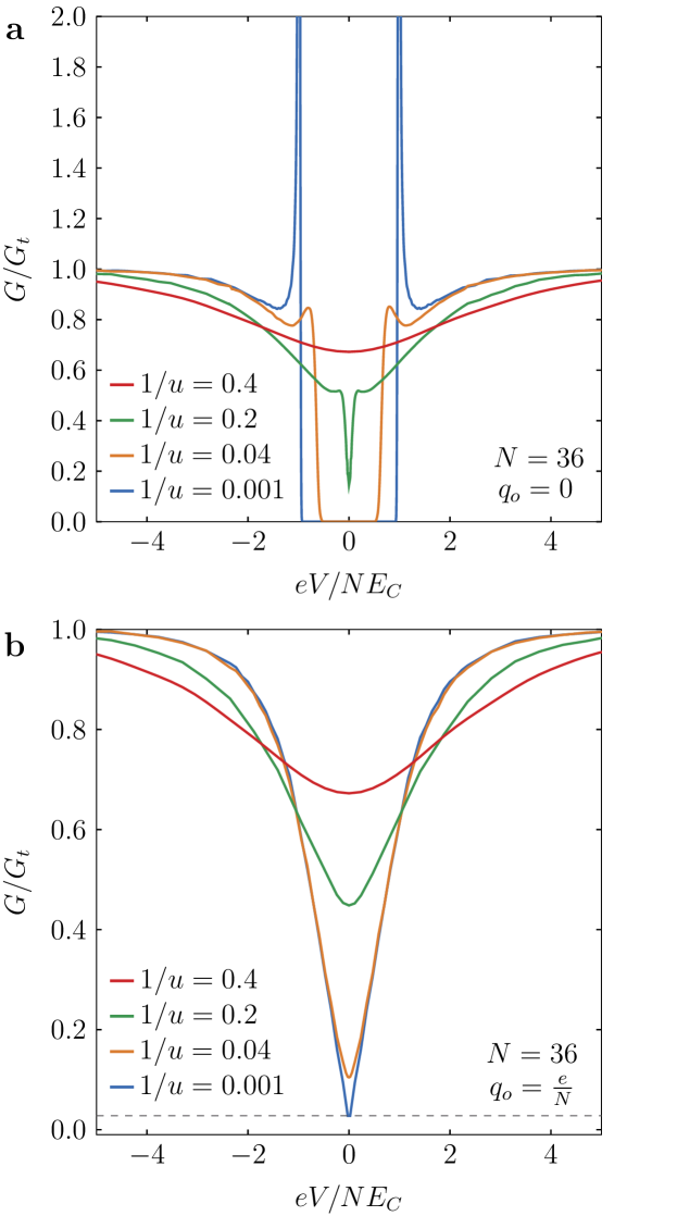
In the low temperature regime, we observe that depends on the offset charge (Fig. 5). The case displayed in Fig. 5a was discussed earlier in the context of charge soliton propagation on tunnel junction chains, where the threshold voltage was found to be at [33, 34], in agreement with our numerical results. In contrast, the case shown in Fig. 5b exhibits a gapless behavior, with no well-defined threshold voltage. However, in agreement with the zero bias conductance data displayed in Fig. 3, a conductance suppression is observed which reaches in the zero temperature limit.
IV The role of random offset charges
Thus far, we considered a uniform offset charge applied on all islands of the CBT. In the absence of externally controlled gate electrodes, the offset charge is randomized by the electrostatic environment [35], which is typically described as an ensemble of two-level charge fluctuators embedded in tunnel barriers or material interfaces [22, 23, 36]. Here, we assume that any rearrangement of offset charges happens much slower than the conductance measurement timescale, which is in the order of a second, so that we can consider a fixed set for a MCMC calculation run, and can average the resulting conductance values to acquire the offset charge-averaged conductance at a given temperature and bias voltage.
Typical charge trap densities exceed m-2 on Si-SiO2 interfaces [37] and in the oxidized surfaces of metal thin layers [36], which, together with a typical metallic surfaces areas exceeding m2 of a single island [18], results in offset charges many orders of magnitude larger than . In a CBT device, where the islands are tunnel coupled to electrodes, this charge will be reduced by tunneling until a stable offset charge configuration is reached. In the single island case () this results in an offset charge uniformly distributed in the range of , since any offset charge outside of this interval would enable a free energy decrease by tunneling of a charge . While the same range is often assumed in the case of long arrays, the system can be trapped in a local minimum of the electrostatic energy with tunneling events towards the global energy minimum being inhibited over realistic timescales in the low temperature regime.
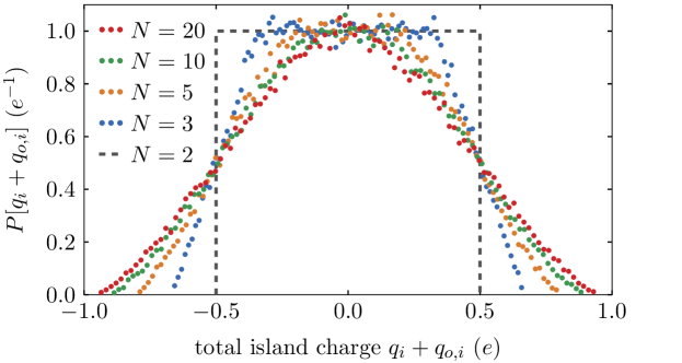
We demonstrate the presence of such charge configurations by initializing arrays of different with a random uniformly distributed with a width of , and a stable offset charge configuration is calculated by minimizing the free energy by a Markov chain of randomly selected tunneling events. The final charge configuration is recorded when all possible tunneling events out of this state increase the electrostatic free energy of the array. We show the resulting probability densities in Fig. 6 with taking the case as a reference. Notably, the resulting offset charges always fall into the window, however we find an increasing probability of being outside of with increasing array size. Based on this numerical result, we follow the above initialization procedure for all MCMC calculations, instead of selecting the offset charge uniformly between as it was done earlier [38].
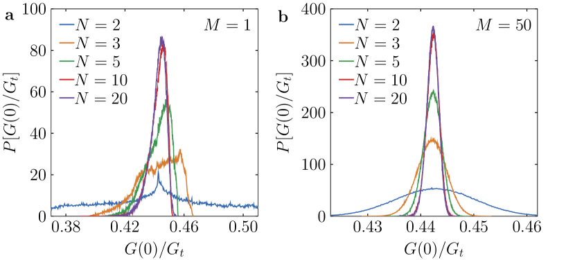
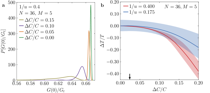
We showcase the statistical variations of due to the random offset charges in Fig. 7a for different array lengths. Remarkably, the resulting distribution narrows with increasing . This is in contrast with the uniform offset charge case shown in Fig. 3, where the difference between the maximum and minimum conductance increases as a function of owing to the strong exponential suppression of fully blockaded arrays.
We note that the width of the conductance distribution further decreases in the typical CBT geometry, where several junction series are connected in parallel in order to increase the device conductance. Assuming an independent offset charge distribution for all arrays, the standard deviation of the conductance is expected to decrease with for an CBT device. We demonstrate this effect by plotting the probability density functions of the sum of randomized conductance values in Fig. 7b.
Both for and , we also observe a saturating distribution when increasing . This defines the long array limit, where the statistical temperature error of the CBT does not depend on the array length. To simplify further analysis and comparison with our previously acquired experimental data [18, 19], we use henceforth, which falls in the long array limit in our temperature regime of interest, . We also note that several other experiments in the millikelvin regime were performed with CBTs of a similar or larger array lengths [14, 15, 17].
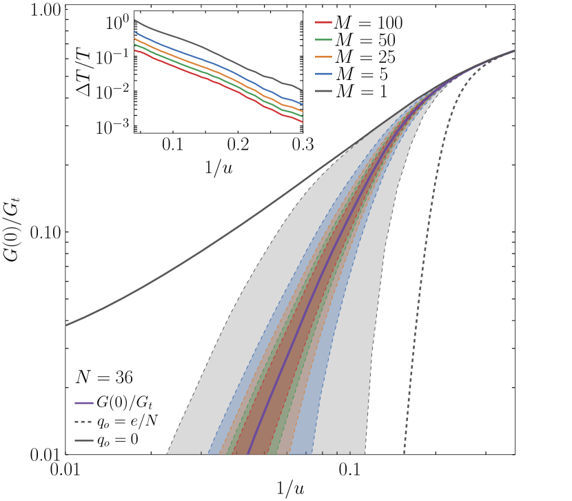
Next, we evaluate the offset-charge averaged conductance as a function of the temperature in a demonstration of Coulomb blockade thermometry beyond the universal temperature regime. Here, we plot the expectation value of as a function of the dimensionless temperature (Fig. 8). Remarkably, the confidence intervals corresponding to remain much narrower than the full conductance window defined by (dashed line) and (solid line). Importantly for thermometry applications, we can evaluate the resulting temperature error , and find that even for , reliable temperature measurements with are possible if , in contrast with the limit calculated earlier for [29]. Furthermore, CBT devices with several junction series in parallel are even more suitable in the low temperature regime: a realistic CBT with reaches the same temperature error at demonstrating the possibility of precision low temperature electron thermometry by using scalable fabrication of large arrays.
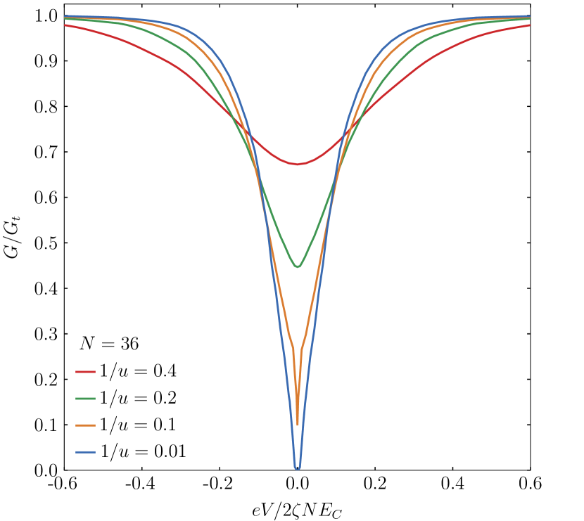
We display the calculated finite bias conductance curves of the same device in Fig. 9, which is the low temperature extension of the results presented in Fig. 4. Remarkably, the full conductance traces remain sensitive to the temperature even when , which allows for a primary calibration of the CBT in the low temperature regime, despite the absence of offset-charge control on the individual islands.
V Disorder in the tunnel junction parameters
Previously we argued that the effect of random offset charges can be mitigated by using devices with large and . However, for realistic device modeling, we also have to consider the non-uniformity in the tunnel junction resistance and island coupling capacitance values. These variations can be due to lithographic inaccuracies as well as thin film thickness variations. Previous studies addressed this error source assuming that the junction area inhomogenity of in-situ created AlOx tunnel barriers dominates [7, 28], equivalent to a constant . However, recent studies demonstrated the spatial variations in the oxide layer thickness [39] and new fabrication techniques utilizing ex-situ via tunnel junctions were developed [18, 40], requiring a separate evaluation of the effects of the capacitance and resistance variations on the CBT accuracy.
We first discuss the effect of the capacitance disorder by calculating a conductance histogram of an and device with a uniform distribution of junction capacitances, (Fig. 10a). Here, corresponds to a homogeneous array, where the conductance distribution is governed by the random offset charges. Increasing results in a broadening of the conductance histogram as well as a quadratic drop in the expectation value of , which translates to a decrease in the inferred temperature (see Fig. 8). We note that we kept constant for different values, using the expectation value in Eq. (5). We show in Fig. 10b that the impact of on thermometry depends on the temperature by displaying the relative temperature error defined as the confidence intervals as a function of at different values. Our results indicate that in the low temperature regime, and realistic capacitance variations of a few percent, the measurement error is dominated by the randomness of the offset charges.
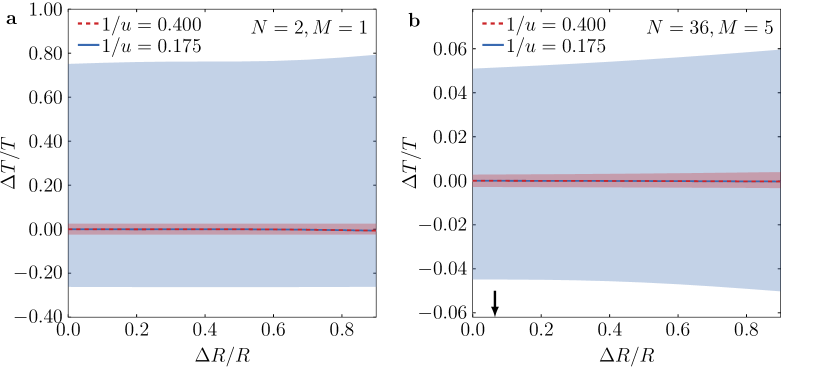
Next, we evaluate the case of variations in the individual tunnel junction resistances, and perform the MCMC simulations with a uniform distribution of with a width of (Fig. 11). The resistance variations cause a weak quadratic decrease in the expectation value of the temperature, however even the extreme case of yields a smaller systematic and statistical error than the capacitance disorder in the regime. When comparing the and (Fig. 11a) single island CBT with the and case (Fig. 11b), we find a marked reduction in the statistical temperature error for the long array, further attesting to the importance of large array devices for low-temperature thermometry.
VI Comparison with experimental data
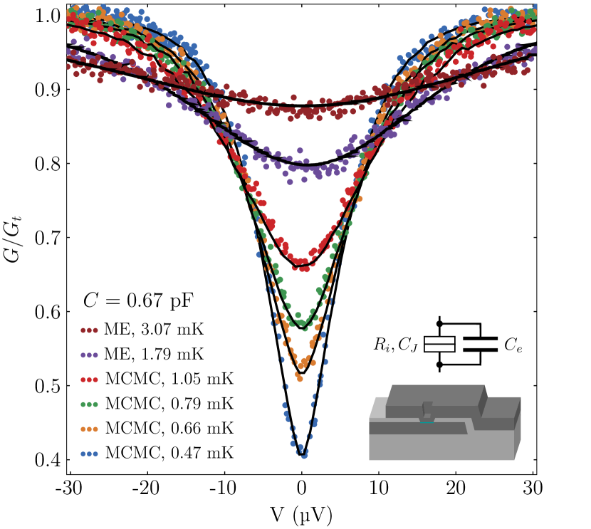
We now demonstrate the correspondence of the MCMC simulations with experimental data taken in the sub-millikelvin electron temperature regime. We fabricated our Coulomb blockade thermometers with ex-situ Al/AlOx/Al via tunnel junctions connecting adjacent Al islands separated by sputtered SiOx interlayer dielectric [18, 40]. This process, in contrast to the frequently used Dolan bridge technique [41], enables an independent tuning of the tunnel junction area and the capacitive coupling between the islands. Crucially for the applicability of our numerical model, our device fulfills the requirement with a large fraction of the island areas overlapping (see the inset of Fig. 12). Our device features tunnel junctions in series and rows in parallel. Electron cooling was performed by on- and off-chip nuclear refrigeration [16], using large volume electrodeposited indium fins. When the nuclear demagnetization was carried out on the device, we observed [19] that the measured electron temperature scales with the effective magnetic field , where is the applied magnetic field and mT is the internal magnetic field corresponding to the quadrupolar crystal field in indium, consistent with prior literature data [42]. We found that the distortion of because of self-heating [43] was negligible. The details of the device fabrication and measurement setup are published elsewhere [18, 19].
First, we measured our CBT in the universal regime, where the ME model provides a reliable calibration of the island capacitance, fF, which we will use as a fixed parameter for the rest of the analysis. In the universal regime, where , we can get reliable fits using the ME model (see the two uppermost curves in Fig. 12). Below this threshold, however, we first fit the temperature comparing the zero bias conductance with the MCMC model prediction (see Fig. 8), and then confirm the validity of the fit in the full voltage bias range (four lower curves in Fig. 12). With this procedure, we get an excellent agreement between our numerical simulations and experimental data down to K corresponding to , where we estimate a relative temperature error of (see Fig. 8). This result demonstrates that accurate Coulomb blockade thermometry is possible outside of the commonly considered universal regime.
Finally, we discuss the temperature error associated with the variations in the tunnel junction parameters and compare the resulting temperature error with the previous result. Based on the maximum alignment error of nm of the laser lithography used to fabricate our device, we infer a relative error in overlap and in the island capacitance (see vertical arrow in Fig. 10b), which in our temperature of interest contributes with less than to the relative temperature error. We characterized our tunnel junctions to exhibit an areal resistance [18], corresponding to (see vertical arrow in Fig. 11b), which has a negligible effect on the temperature error. Our analysis attests to the insensitivity of CBTs to realistic fabrication inaccuracies in the low temperature regime, in agreement with similar numerical studies in the universal regime [5, 7, 20, 32].
VII Corrections with a finite gating capacitance
We now turn to the case where the island gating capacitance is finite, but still much less than the capacitances between the islands (Fig. 1). First, we establish the validity of this limit by estimating the self-capacitance of the islands in our experiments [18, 19], which is assumed to be dominated by the indium cooling fins [18] with linear dimensions of m3. To provide an estimate, we use the self-capacitance of a cube [44] with m side yielding fF and .
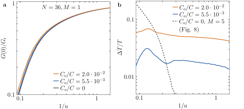
We use the numerical model discussed in Section 3 using the capacitance matrix (see Eq. [2]) with a modified . As we demonstrated in Fig. 10 and Fig. 11, the leading term in statistical variations is caused by the random offset charges, therefore we evaluate the offset-charge averaged zero bias conductance curves as a function of temperature for finite ratios while keeping constant with no disorder in the capacitance values and tunnel junction resistances. Similarly to our other calculations, we set to enable a direct comparison with our experiments.
We summarize our calculations in Fig. 13, where we display the temperature dependence of the normalized zero bias conductance (Fig. 13a) for a ratio of and , which we compare to the model also shown in Fig. 8. We recover the high temperature, universal regime, where the curves merge, however we find an increasing systematic deviation when lowering the temperature to the the intermediate [29] and to the low temperature limit. In Fig. 13b, we characterize the resulting relative temperature error resulting from using the model in case of these two finite ratios. We note that , thus neglecting yields an overestimate of the device temperature. Our numerical results show that this error is of the order of in our temperature regime of interest, and it increases with the ratio of the device, demonstrating the importance of the specific CBT device design for ulta-low temperature thermometry.
We conclude this analysis by comparing this systematic deviation to the statistical uncertainty caused by the random offset charges for , relevant for our device. We find that in the low temperature limit , the statistical uncertainty dominates. This is in contrast to the intermediate regime , where the finite ratio plays a more important role. Our numerical results demonstrate that CBT devices with large area overlaps between neighboring islands [15, 18] are preferred in the intermediate regime to devices with shadow-evaporated tunnel junctions [20] and large surface area cooling fins [16] featuring higher ratios.
VIII Conclusions
Using Markov-chain Monte Carlo simulations, we demonstrated that Coulomb blockade thermometry can be extended beyond the universal regime. Our results show that long arrays with many islands in series benefit from the narrowing total conductance distribution even in the case of random offset charges, and the statistical temperature errors are further reduced by adding several junctions series in parallel, which is a typical geometry for practical CBTs. These contributions lead up to a factor of four increase in the usable temperature range of a CBT with a realistic number of tunnel junctions, impacting precision thermometry applications. We demonstrated the applicability of the numerical results to experimental data taken in the sub-millikelvin temperature regime. These temperatures fall outside of the universal regime for a CBT featuring a charging energy exceeding mK, which is necessary to perform a primary calibration at electron temperatures in the range of mK attainable in commercial dilution refrigerators. Finally, we showed that at sub-millikelvin temperatures, device designs yielding a low gate capacitance ratio are necessary to suppress systematic temperature errors stemming from a finite .
Data availability
Raw datasets and computer code are available at the Zenodo repository [45].
Acknowledgements.
The authors thank J. Pekola for fruitful discussions. This work was supported by the Netherlands Organization for Scientific Research (NWO) and by the European Research Council under the European Union’s Horizon 2020 research and innovation programme, grant number 804988.Conflict of interest
The authors declare no conflict of interest.
References
- [1] D.V. Averin, K.K. Likharev, Single electronics: A correlated transfer of single electrons and Cooper pairs in systems of small tunnel junctions (Elsevier, 1991), chap. 6, pp. 173–272
- [2] H. Grabert, M.H. Devoret, Single Charge Tunneling: Coulomb Blockade Phenomena In Nanostructures (Springer US, 1992)
- [3] M. Field, C.G. Smith, M. Pepper, D.A. Ritchie, J.E.F. Frost, G.A.C. Jones, D.G. Hasko, Phys. Rev. Lett. 70, 1311 (1993)
- [4] T.A. Fulton, G.J. Dolan, Phys. Rev. Lett. 59, 109 (1987)
- [5] J.P. Pekola, K.P. Hirvi, J.P. Kauppinen, M. Paalanen, Phys. Rev. Lett. 73, 2903 (1994)
- [6] J.P. Pekola, J. Toppari, J. Kauppinen, K. Kinnunen, A. Manninen, A. Jansen, Journal of Applied Physics 83(10), 5582 (1998)
- [7] O. Hahtela, M. Meschke, A. Savin, D. Gunnarsson, M. Prunnila, J. Penttilä, L. Roschier, M. Heinonen, A. Manninen, J. Pekola, in AIP Conference Proceedings, vol. 1552 (AIP, 2013), vol. 1552, pp. 142–147
- [8] T. Bergsten, T. Claeson, P. Delsing, Journal of Applied Physics 86(7), 3844 (1999)
- [9] T. Bergsten, T. Claeson, P. Delsing, Applied Physics Letters 78(9), 1264 (2001)
- [10] M. Meschke, J. Engert, D. Heyer, J. Pekola, International Journal of Thermophysics 32(7-8), 1378 (2011)
- [11] O. Hahtela, E. Mykkänen, A. Kemppinen, M. Meschke, M. Prunnila, D. Gunnarson, L. Roschier, J. Penttilä, J. Pekola, Metrologia 54, 69 (2017)
- [12] T. Knuuttila, K. Nummila, W. Yao, J. Kauppinen, J. Pekola, Physica E: Low-dimensional Systems and Nanostructures 3(4), 224 (1998)
- [13] J.P. Pekola, T. Holmqvist, M. Meschke, Phys. Rev. Lett. 101, 206801 (2008)
- [14] L. Casparis, M. Meschke, D. Maradan, A.C. Clark, C.P. Scheller, K.K. Schwarzwälder, J.P. Pekola, D. Zumbühl, Rev. Sci. Instr. 83(8), 083903 (2012)
- [15] D. Bradley, R. George, D. Gunnarsson, R. Haley, H. Heikkinen, Y. Pashkin, J. Penttilä, J. Prance, M. Prunnila, L. Roschier, M. Sarsby, Nature communications 7, 10455 (2016)
- [16] M. Palma, C. Scheller, D. Maradan, A. Feshchenko, M. Meschke, D. Zumbühl, Appl. Phys. Lett. 111(25), 253105 (2017)
- [17] D. Bradley, A. Guénault, D. Gunnarsson, R. Haley, S. Holt, A. Jones, Y.A. Pashkin, J. Penttilä, J. Prance, M. Prunnila, L. Roschier, Scientific Reports 7, 45566 (2017)
- [18] N. Yurttagül, M. Sarsby, A. Geresdi, Phys. Rev. Applied 12, 011005 (2019)
- [19] M. Sarsby, N. Yurttagül, A. Geresdi, Nature Communications 11(1), 1492 (2020)
- [20] M. Meschke, A. Kemppinen, J. Pekola, Phil. Trans. R. Soc. A 374, 20150052 (2016)
- [21] L. Geerligs, V. Anderegg, J. Mooij, Physica B: Condensed Matter 165-166, 973 (1990). LT-19
- [22] G. Zimmerli, T.M. Eiles, R.L. Kautz, J.M. Martinis, Applied Physics Letters 61(2), 237 (1992)
- [23] N.M. Zimmerman, J.L. Cobb, A.F. Clark, Phys. Rev. B 56, 7675 (1997)
- [24] F. Giazotto, T.T. Heikkilä, A. Luukanen, A.M. Savin, J.P. Pekola, Rev. Mod. Phys. 78, 217 (2006)
- [25] G. Pickett, C. Enss, Nat. Rev. Mater. 3, 18012 (2018)
- [26] A.T. Jones, C.P. Scheller, J.R. Prance, Y.B. Kalyoncu, D.M. Zumbühl, R.P. Haley, Journal of Low Temperature Physics 201(5), 772 (2020)
- [27] G.L. Ingold, Y.V. Nazarov, Charge Tunneling Rates in Ultrasmall Junctions (Springer US, Boston, MA, 1992), pp. 21–107
- [28] K.P. Hirvi, J.P. Kauppinen, A.N. Korotkov, M.A. Paalanen, J.P. Pekola, Applied Physics Letters 67(14), 2096 (1995)
- [29] A. Feshchenko, M. Meschke, D. Gunnarsson, M. Prunnila, L. Roschier, J. Penttilá, J. Pekola, Journal of Low Temperature Physics 173(1-2), 36 (2013)
- [30] N. Bakhvalov, G. Kazacha, K. Likharev, S. Serdyukova, Sov. Phys. JETP 68(3), 581 (1989)
- [31] C. Wasshuber, Computational Single-Electronics, 1st edn. (Springer, 2001)
- [32] K. Hirvi, M. Paalanen, J. Pekola, J. Appl. Phys. 80(1), 256 (1996)
- [33] M. Amman, E. Ben-Jacob, K. Mullen, Phys. Lett. A 142(6), 431 (1989)
- [34] G.Y. Hu, R.F. O’Connell, Phys. Rev. B 49, 16773 (1994)
- [35] P. Dutta, P.M. Horn, Rev. Mod. Phys. 53, 497 (1981)
- [36] N.M. Zimmerman, W.H. Huber, B. Simonds, E. Hourdakis, A. Fujiwara, Y. Ono, Y. Takahashi, H. Inokawa, M. Furlan, M.W. Keller, Journal of Applied Physics 104(3), 033710 (2008)
- [37] Y. Cheng, Progress in Surface Science 8, 181 (1977)
- [38] J. Johansson, D. Haviland, Phys. Rev. B 63, 014201 (2000)
- [39] L.J. Zeng, S. Nik, T. Greibe, P. Krantz, C.M. Wilson, P. Delsing, E. Olsson, Journal of Physics D: Applied Physics 48(39), 395308 (2015)
- [40] M. Prunnila, M. Meschke, D. Gunnarson, S. Enouz-Vedrenne, J. Kivioja, J. Pekola, Journal of Vacuum Science and Technology B 28, 1026 (2010)
- [41] G.J. Dolan, Applied Physics Letters 31(5), 337 (1977)
- [42] Y. Tang, E. Adams, K. Uhlig, D. Bittner, J. Low Temp. Phys. 60, 352 (1985)
- [43] R.L. Kautz, G. Zimmerli, J.M. Martinis, Journal of Applied Physics 73(5), 2386 (1993)
- [44] C.O. Hwang, M. Mascagni, Journal of Applied Physics 95(7), 3798 (2004)
- [45] N. Yurttagül, M. Sarsby, A. Geresdi. Coulomb blockade thermometry beyond the universal regime, raw data and software. URL http://dx.doi.org/10.5281/zenodo.3831241