Intrinsic piezoelectricity in monolayer (X=Ti, Zr, Hf, Cr, Mo and W)
Abstract
Motived by experimentally synthesized (\textcolor[rgb]0.00,0.00,1.00Science 369, 670-674 (2020)), the intrinsic piezoelectricity in monolayer (X=Ti, Zr, Hf, Cr, Mo and W) are studied by density functional theory (DFT). Among the six monolayers, the has the best piezoelectric strain coefficient of 1.24 pm/V, and the second is 1.15 pm/V for . Taking as a example, strain engineering is applied to improve . It is found that tensile biaxial strain can enhance of , and the at 4% can improve by 107% with respect to unstrained one. By replacing the N by P or As in , the can be raise substantially. For and , the is as high as 4.93 pm/V and 6.23 pm/V, which is mainly due to smaller and very small minus or positive ionic contribution to piezoelectric stress coefficient with respect to . The discovery of this piezoelectricity in monolayer enables active sensing, actuating and new electronic components for nanoscale devices, and is recommended for experimental exploration.
pacs:
71.20.-b, 77.65.-j, 72.15.Jf, 78.67.-n Email:sandongyuwang@163.comI Introduction
Piezoelectric materials can convert mechanical energy into electrical energy and vice versa, and the piezoelectricity of two-dimensional (2D) materias has been widely investigatedq4 in recent years. Experimentally, the existence of piezoelectricity of q5 ; q6 , MoSSeq8 and q8-1 has significantly promoted development of the piezoelectricity of 2D materials. It has been reported that a large number of 2D materials have significant piezoelectric coefficients, such as transition metal dichalchogenides (TMD), Janus TMD, group IIA and IIB metal oxides, group-V binary semiconductors and group III-V semiconductorsq7 ; q7-1 ; q7-2 ; q7-3 ; q7-4 ; q9 ; q10 ; q11 ; q12 ; qr , the monolayer SnSe, SnS, GeSe and GeS of which possess giant piezoelectricity, as high as 75-251 pm/Vq10 . Due to different crystal symmetry, a only in-plane piezoelectricity, both in-plane and out-of-plane piezoelectricity, or a pure out-of-plane piezoelectricity can exit, and the corresponding example is TMD monolayersq9 , many 2D Janus materialsq7 ; q7-3 and penta-grapheneq7-4 . The strain-tuned piezoelectric response of r1 , AsPq7-1 , SnSeq7-1 and Janus TMD monolayersr3 have been performed by the first-principle calculations, and it is proved that strain can improve the piezoelectric strain coefficients.
Recently, the layered 2D has been synthesized by chemical vapor deposition (CVD)msn . Many other 2D materials with a general formula of have been predicted by DFT calculationsmsn , where X represents an early transition metal (W, V, Nb, Ta, Ti, Zr, Hf, or Cr), Y is Si or Ge, and M stands for N, P, or As. In this work, the piezoelectric properties of monolayer (X=Ti, Zr, Hf, Cr, Mo and W) are studied by using density functional perturbation theory (DFPT)pv6 . The independent in-plane piezoelectric constants is predicted to be 0.777 pm/V to 1.241 pm/V, which are smaller than ones of many other 2D materialsq7 ; q7-3 ; q9 ; q10 ; q11 . Using as a example, strain engineering is proposed to produce improved piezoelectric properties. It is found that increasing strain can improve due to reduced - and enhanced , and the band gap decreases. Calculated results show that and have more better than (X=Ti, Zr, Hf, Cr, Mo and W), which is mainly because they are more softer, and their ionic parts have very small minus contribution () or positive contribution () to . Our calculations show that the (X=Ti, Zr, Hf, Cr, Mo or W; Y=Si or Ge; and M=N, P or As) materials may be promising candidates for piezoelectric applications.
| Name | - | |||||||
|---|---|---|---|---|---|---|---|---|
| 2.931 | 6.908 | 1.629 | 1.628 | 0.033 | 326.239 | 2.712 | 0.831 | |
| 3.032 | 7.035 | 1.629 | 1.625 | 0.056 | 287.008 | 2.229 | 0.777 | |
| 3.022 | 7.000 | 1.802 | 1.789 | 0.183 | 303.898 | 3.199 | 1.053 | |
| 2.844 | 6.869 | 0.498 | 0.499 | 0.063 | 358.021 | 4.442 | 1.241 | |
| 2.909 | 7.004 | 1.747 | 1.746 | 0.130 | 383.982 | 4.398 | 1.145 | |
| 2.912 | 7.014 | 2.083 | 2.074 | 0.399 | 403.227 | 3.138 | 0.778 |
II Computational detail
We perform DFT calculations1 using the projector-augmented wave method as implemented in the plane-wave code VASPpv1 ; pv2 ; pv3 . For the structural relaxation and the calculations of the elastic and piezoelectric tensors, we use the popular generalized gradient approximation of Perdew, Burke and Ernzerhof (GGA-PBE)pbe as the exchange-correlation functional. For energy band calculations, the spin orbital coupling (SOC) is also taken into account. A cutoff energy of 500 eV for the plane wave basis set is used to ensure an accurate DFT calculations. A vacuum spacing of more than 32 is adopted to reduce the interactions between the layers, which is key to attain accurate . The total energy convergence criterion is set to eV, and the Hellmann-Feynman forces on each atom are less than 0.0001 . The coefficients of the elastic stiffness tensor are calculated by using strain-stress relationship (SSR), and the piezoelectric stress coefficients are attained by DFPT methodpv6 . The Brillouin zone sampling is done using a Monkhorst-Pack mesh of 15151 for , and 9161 for . The 2D elastic coefficients and piezoelectric stress coefficients have been renormalized by the length of unit cell along z direction (): = and =.
III Symmetry Analysis
The relaxed-ion piezoelectric stress tensors and strain tensor , from the sum of ionic and electronic contributions , is defined as:
| (1) |
and
| (2) |
where , and are polarization vector, strain and stress, respectively. The and are related via the elastic stiffness tensor . Monolayer belongs to the point group. Employing the Voigt notation, if we only consider in-plane strain componentsq7 ; q9 ; q10 ; q11 ; q12 for 2D materials, the , and become into:
| (3) |
| (4) |
| (5) |
Here, the only in-plane is derived by =:
| (6) |
IV Main calculated results
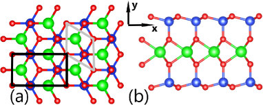
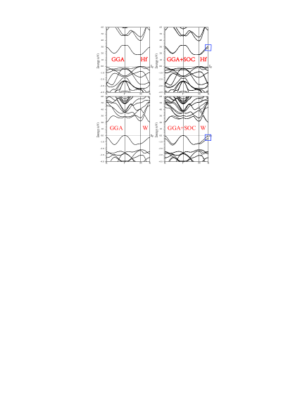
The geometric structures of the monolayer are plotted in Figure 1, which consist of seven atomic layers of N-Si-N-X-N-Si-N (a layer sandwiched between two Si-N bilayers). The optimized structural parameters of (X=Ti, Zr, Hf, Cr, Mo and W) (in Table 1) agree well with the previous calculated resultsmsn . The electronic band structures of these monolayers are also calculated using GGA and GGA+SOC, and the representative and monolayers are shown in Figure 2. The energy bands of (X=Ti, Zr, Cr, Mo) are plotted in Fig.1 and Fig.2 of supplementary materials. Compared to (X=Ti, Zr, Hf), additional two electrons are added for (X=Cr, Mo and W), and then the first two conduction bands are filled. Their corresponding gaps (GGA and GGA+SOC) and spin-orbital splitting at K point are summarized in Table 1. It is clearly seen that the difference of gap between GGA and GGA+SOC is very little. Calculated results show that the magnitude of spin-orbital splitting accords with the atomic mass of X.
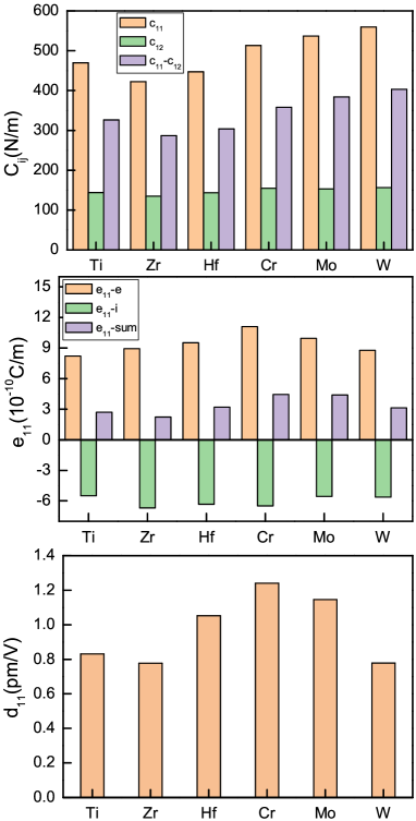
Due to hexagonal symmetry, the two independent elastic stiffness coefficients ( and ) are calculated by SSR, and all calculated elastic coefficients satisfy the Born stability criteriaela . The elastic stiffness coefficients (, and -) are show in Figure 3. These elastic constants are larger than ones of most 2D materials, like TMD, metal oxides, and III-V semiconductor materialsq9 ; q11 , indicating that these 2D monolayers are more rigid than other 2D materials. The piezoelectric stress coefficients of monolayer are calculated by DFPT, using the rectangle supercell. Based on Equation 6, the piezoelectric strain coefficients are attained. The piezoelectric coefficients and , and the ionic contribution and electronic contribution to are plotted in Figure 3. Some key data are also listed in Table 1. For all six monolayers, it is clearly seen that the ionic contribution and electronic contribution to is opposite. The entire range of calculated is from 2.229 C/m to 4.442 C/m, while the ranges from 0.777 pm/V to 1.241 pm/V. Their are smaller than ones of TMD monolayers (2.12 pm/V to 13.45 pm/V)q9 ; q11 . For example, the of (4.442 C/m) and (4.398 C/m) are larger than one of (3.64 C/m), but their (1.241 pm/V and 1.145 pm/V) are smaller than one of (3.73 pm/V)q9 ; q11 , which is due to larger -. Among all studied six monolayers, the monolayer has the best .
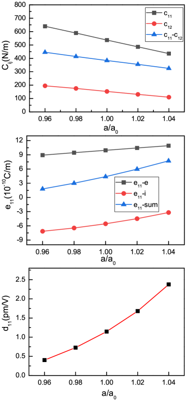
The of monolayer is very small, and strain engineering is proposed to enhance their piezoelectric properties, which has been proved to a very effective wayr1 ; q7-1 ; r3 . Here, we use experimentally synthesized as an example to study the strain effects on piezoelectric properties. Due to symmetry, biaxial strain can not induce polarization, not like uniaxial strain. We only consider biaxial strain effects on piezoelectric properties of , and the elastic constants -, piezoelectric coefficients and , and the ionic contribution and electronic contribution to of monolayer as a function of biaxial strain are plotted in Figure 4. When the strain varies from -4% to 4%, the - decreases, and the increases, which gives rise to improved based on Equation 6. At 4% strain, the is 2.375 pm/V, which is more than twice as large as unstrained one (1.145 pm/V). Similar biaxial strain-improved can be found in monolayer g- and gsd . It is found that both ionic contribution and electronic contribution to have positive influence to improve of monolayer , which is different from monolayer g- and gsd .

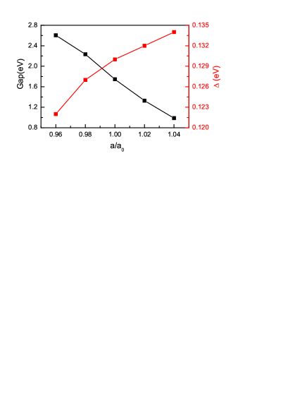
At applied strain, the monolayer exhibits piezoelectricity, which should have a band gap. The gap and spin-orbital splitting at K point as a function of strain are plotted in Figure 5, and the strain-related energy bands of are plotted in Fig.3 of supplementary materials. It is found that the gap decreases from 2.605 eV (-4%) to 0.988 eV (4%), while the increases from 0.122 eV to 0.134 eV. The position of conduction band minimum (CBM) do not change from -4% to 4%, but the position of valence band maximum (VBM) changes from K point to point. The valence bands convergence can be observed at about -2% strain due to almost the same energy between K point and point, which is in favour of better p-type Seebeck coefficient. Similar strain-induced bands convergence can be observed in many 2D materials like gsd1 .
To further enhance piezoelectric properties, using elements of group IVA and elements of group VA to replace the Si and N elements in experimentally synthesized , the monolayer , and are proved to be stablemsn . The elastic constants -, piezoelectric coefficients and , and the ionic contribution and electronic contribution to of monolayer , , and are plotted in Figure 6. It is clearly seen that monolayer and have very higher than , and they are 4.93 pm/V and 6.23 pm/V, which are comparable to one of most TMD monolayersq9 . One reason of the high for monolayer and is that monolayer and have more smaller and than , which leads to smaller -. Another reason is that the minus of the ionic contribution to of monolayer is very small, and the ionic contribution is positive for monolayer . The of monolayer is 1.83 pm/V. which is close to one of .
V Conclusion
Significant progress has been achieved in synthetizing monolayer with a non-centrosymmetric structure, which allows it to be piezoelectric. Here, the piezoelectric properties of monolayer (X=Ti, Zr, Hf, Cr, Mo and W) are studied by using first-principles calculations. In the considered six materials, the is predicted to have the best of 1.24 pm/V, and the second is 1.15 pm/V for experimentally synthesized . It is found that strain engineering can improve of , and the at 4% biaxial strain can improve by 107%. Compared to monolayer (X=Ti, Zr, Hf, Cr, Mo and W), the monolayer , and have more higher , and the of is as high as 6.23 pm/V. Owing to the recent CVD growth in monolayer , it is expected that these monolayers (X=Ti, Zr, Hf, Cr, Mo or W; Y=Si or Ge; and M=N, P or As) may be put to a wide practical piezoelectric use in the future.
Acknowledgements.
This work is supported by the Natural Science Foundation of Shaanxi Provincial Department of Education (19JK0809). We are grateful to the Advanced Analysis and Computation Center of China University of Mining and Technology (CUMT) for the award of CPU hours and WIEN2k/VASP software to accomplish this work.References
- (1) W. Wu and Z. L. Wang, Nat. Rev. Mater. 1, 16031 (2016).
- (2) W. Wu, L. Wang, Y. Li, F. Zhang, L. Lin, S. Niu, D. Chenet, X. Zhang, Y. Hao, T. F. Heinz, J. Hone and Z. L. Wang, Nature 514, 470 (2014).
- (3) H. Zhu, Y. Wang, J. Xiao, M. Liu, S. Xiong, Z. J. Wong, Z. Ye, Y. Ye, X. Yin and X. Zhang, Nat. Nanotechnol. 10, 151 (2015).
- (4) A. Y. Lu, H. Zhu, J. Xiao, C. P. Chuu, Y. Han, M. H. Chiu, C. C. Cheng, C. W. Yang, K. H. Wei, Y. Yang, Y. Wang, D. Sokaras, D. Nordlund, P. Yang, D. A. Muller, M. Y. Chou, X. Zhang and L. J. Li, Nat. Nanotechnol. 12, 744 (2017).
- (5) M. Dai, Z. Wang, F. Wang, Y. Qiu, J. Zhang, C. Y. Xu, T. Zhai, W. Cao, Y. Fu, D. Jia, Y. Zhou, and P. A. Hu, Nano Lett. 19, 5416 (2019).
- (6) L. Dong, J. Lou and V. B. Shenoy, ACS Nano, 11, 8242 (2017).
- (7) S. D. Guo, X. S. Guo, Y. Y. Zhang and K. Luo, J. Alloy. Compd. 822, 153577 (2020).
- (8) Y. Xu, Z. Q. Li, C. Y. He, J. Li, T. Ouyang, C. X. Zhang, C. Tang and J. X. Zhong Appl. Phys. Lett. 116, 023103 (2020).
- (9) S. D. Guo, X. S. Guo, Z. Y. Liu and Y. N. Quan, J. Appl. Phys. 127, 064302 (2020).
- (10) S. D. Guo and S. Q. Wang, J. Phys. Chem. Solids 140, 109375 (2020).
- (11) M. N. Blonsky, H. L. Zhuang, A. K. Singh and R. G. Hennig, ACS Nano, 9, 9885 (2015).
- (12) R. X. Fei, We. B. Li, J. Li and L. Yang, Appl. Phys. Lett. 107, 173104 (2015)
- (13) K. N. Duerloo, M. T. Ong and E. J. Reed, J. Phys. Chem. Lett. 3, 2871 (2012).
- (14) Y. Chen, J. Y. Liu, J. B. Yu, Y. G. Guo and Q. Sun, Phys. Chem. Chem. Phys. 21, 1207 (2019).
- (15) Y. G. Guo, H. Q. Zhu and Q. Wang, ACS Appl. Mater. Interfaces 11, 1033 (2019).
- (16) N. Jena, Dimple, S. D. Behere and A. D. Sarkar, J. Phys. Chem. C 121, 9181 (2017).
- (17) Dimple, N. Jena, A. Rawat, R. Ahammed, M. K. Mohanta and A. D. Sarkar, J. Mater. Chem. A 6, 24885 (2018).
- (18) Y. L. Hong, Z. B. Liu, L. Wang et al., Science 369, 670 (2020).
- (19) X. Wu, D. Vanderbilt and D. R. Hamann, Phys. Rev. B 72, 035105 (2005).
- (20) P. Hohenberg and W. Kohn, Phys. Rev. 136, B864 (1964); W. Kohn and L. J. Sham, Phys. Rev. 140, A1133 (1965).
- (21) G. Kresse, J. Non-Cryst. Solids 193, 222 (1995).
- (22) G. Kresse and J. Furthmller, Comput. Mater. Sci. 6, 15 (1996).
- (23) G. Kresse and D. Joubert, Phys. Rev. B 59, 1758 (1999).
- (24) J. P. Perdew, K. Burke and M. Ernzerhof, Phys. Rev. Lett. 77, 3865 (1996).
- (25) R. C. Andrew, R. E. Mapasha, A. M. Ukpong and N. Chetty, Phys. Rev. B 85, 125428 (2012).
- (26) S. D. Guo, W. Q. Mu and Y. T. Zhu, in preparation.
- (27) S. D. Guo, J. Mater. Chem. C, 4, 9366 (2016).