Prediction of Tunable Spin-Orbit Gapped Materials for Dark Matter Detection
Abstract
New ideas for low-mass dark matter direct detection suggest that narrow band gap materials, such as Dirac semiconductors, are sensitive to the absorption of meV dark matter or the scattering of keV dark matter. Here we propose spin-orbit semiconductors – materials whose band gap arises due to spin-orbit coupling – as low-mass dark matter targets owing to their band gaps. We present three material families that are predicted to be spin-orbit semiconductors using Density Functional Theory (DFT), assess their electronic and topological features, and evaluate their use as low-mass dark matter targets. In particular, we find that that the tin pnictide compounds are especially suitable having a tunable range of meV-scale band gaps with anisotropic Fermi velocities allowing directional detection. Finally, we address the pitfalls in the DFT methods that must be considered in the ab initio prediction of narrow-gapped materials, including those close to the topological critical point.
I Introduction
New models of dark matter (DM) offer the tantalizing possibility that direct detection is within the realms of short and modestly scaled experiments.Battaglieri et al. (2017) Recent models assigning DM mass to the sub-GeV range have incentivized the design of detection experiments that push the bounds of mass sensitivity. The observation of the small energy depositions associated with light masses requires creative materials solutions, with recently proposed targets including scintillators, Dirac materials, superconductors, polar materials and superfluid helium.Derenzo et al. (2017); Hochberg et al. (2018, 2016a, 2016b); Knapen et al. (2018, 2017); Trickle et al. (2020); Griffin et al. (2020)
Charge-based detectors rely on scattering or absorption events to excite charge carriers across an energy gap that is tailored to the expected energy deposition.Hochberg et al. (2017); Essig et al. (2016) Semiconductors with meV-scale band gaps are therefore suitable for the absorption of DM with meV mass and scattering of DM with keV mass due to the meV magnitude kinetic energy. Although the energy gap imposes a threshold on the detectable DM mass, a finite gap is necessary for decoupling a DM signal from thermal noise.Hochberg et al. (2016b) Therefore, semiconductors with ultra-narrow band gaps are sought to maximize the reach of direct detection experiments. Narrow band gap semiconductors are also desired for infrared radiation detection, especially for sensitivity to long wavelengths.Baker (2017) Furthermore, small band gaps are often linked to high-performance of conventional thermoelectric materials.Shi et al. (2016)
A special class of small band gap compounds, (gapped) Dirac materials, have been identified as promising DM detection targets providing high sensitivity for absorption events.Hochberg et al. (2018) For maximal DM scattering rate, the target material should have a Fermi velocity kinematically matched to the DM velocity, which is serendipitously of the order of , similar to the ranges reported in Dirac materials.Hochberg et al. (2018)
Several candidates for low-mass DM detection based on low band gap, Dirac-like dispersions have been explored,Geilhufe et al. (2018, 2020); Sánchez-Martínez et al. (2019) with topological ZrTe5 emerging as a leading candidate.Hochberg et al. (2018) ZrTe5 possesses Dirac nodes that are gapped out to 20 meV when spin-orbit coupling (SOC) is included in calculations.Nair et al. (2018) However, ZrTe5 is difficult to obtain in large single-crystal form as it is a layered van der Waals material, and in addition, its electronic properties have been shown to strongly depend on structure, synthesis conditions and temperature.Xu et al. (2018); Monserrat and Narayan (2019) Therefore, alternative low-band gap materials which can be synthesized reliably in single-crystal form are needed for next-generation low mass dark matter experiments.
However, any computational searches for such low band gap materials will be mired with the well-documented band gap problem of standard Density Functional Theory (DFT) methods. Semilocal DFT exchange-correlation functionals include a spurious self-interaction in the occupied states, resulting in the over-delocalization of charge densities; in addition, semilocal functionals do not feature a discontinuity in the potential with change in particle number, resulting in significant underestimation of band gaps.Perdew and Levy (1983); Perdew (1986); Mori-Sánchez et al. (2008) In many materials the electron delocalization is better treated with a screened hybrid functional, which can improve the description due to a reduction in the self-interaction error, and open the band gap.Krukau et al. (2006) Hybrid functionals have a greater computational cost than semilocal DFT, but are considerably cheaper than the more chemically accurate GW methods, whilst providing comparable results.Garza and Scuseria (2016); Crowley et al. (2016)
In this work we propose an alternative method to circumvent this common failure of DFT in band gap prediction. Here we propose to search instead for ‘spin-orbit semiconductors’ – these would-be metals are metallic without SOC and are gapped out upon the inclusion of SOC. A familiar example occurs in graphene which is a Dirac semimetal when SOC is not included, opening up to a gap of tens of eV with SOC. In fact, the concept of a spin-orbit gap, that is a band gap that is opened only when SOC interactions are included, is closely related to the topological quantum phase transition, whereby a topological material, such as a Dirac semimetal, can become a trivial insulator by manipulation of the symmetry of the crystal potential. Such spin-orbit gaps can be predicted by DFT calculations by simply comparing band structures with SOC included and not included. Band gaps are of the order of the strength of spin-orbit coupling, hence in the meV range suitable for low-mass dark matter detector candidates.
In this work, we examine the use of a spin-orbit gap, as predicted by DFT, for selecting candidate materials for dark matter detection targets. We choose three materials predicted to have a spin-orbit gap and evaluate their electronic structure, using generalized gradient approximation (GGA) and hybrid functional levels of theory, and their closeness to the topological point. Following the computational methodology, the results and discussion are divided into three sections: A. Candidate Materials, B. Suitability as Dark Matter Targets and C. Theoretical Predictions of Spin-Orbit Gapped Materials.
II Computational Methodology
First-principles calculations based on Density Functional Theory (DFT) were performed using the Vienna Ab initio Simulation Package (vasp)Kresse and Hafner (1993, 1994); Kresse and Furthmüller (1996a, b) with projector augmented wave (PAW) pseudopotentials.Blöchl (1994); Kresse and Joubert (1999) For each element, the states included as valence were s and p for alkali metals, alkaline earth metals, metalloids and non-metals, and s, p and d for transition and post-transition metals. Energy cutoff and k-point convergence testing was carried out on each material and parameters were chosen for a convergence of at least 1 meV per formula unit. These parameters are given in SI Table 1. The convergence criteria for the electronic self-consistent loop was set to eV. Structural optimizations were done using the Perdew-Becke-Ernzerhof (PBE)Perdew et al. (1996) exchange-correlation functional until the residual forces on the ions were less than .
Electronic density of states and band structures were calculated with both the PBE functional and the HSE06 hybrid functionalHeyd et al. (2003, 2006) on top of the PBE optimized structures. Band structures were calculated both with and without spin-orbit coupling interactions, which were included self-consistently.Steiner et al. (2016) The software sumo was used to plot the electronic structures.M Ganose et al. (2018)
III Results and discussion
III.1 Candidate Materials
We used an existing data set of materialspri (2019) which had electronic transport properties calculated by DFT, using the PBE functional, to select three candidate materials which were metallic (zero gap) without including SOC, and opened up a finite gap with SOC included: \ceCuInTe2, \ceSrSn2As2 and \ceLi6Bi2O7. We ensured that these compounds contained at least one element with a sizable spin-orbit coupling magnitude and had a calculated energy above hull less than 0.02 eV. We also investigated materials which were isostructural to these three candidates, with cation and anion substitutions chosen to vary the spin-orbit interaction strength. In a spin-orbit gapped material, substitutions of heavier elements would be expected to widen the band gap due to the increase in SOC-strength with atomic mass.Herman et al. (1963) We report the trends in electronic structure with these substitutions and their effectiveness in tuning the band gap and hence sensitivity to various DM masses.
III.1.1 Copper indium chalcogenides
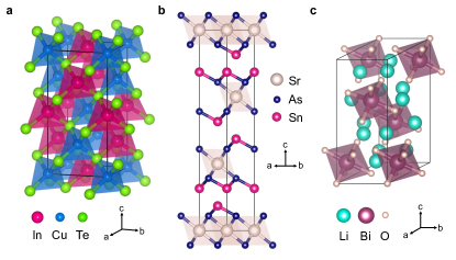
Structural details: Copper indium ditelluride, \ceCuInTe2, has the chalcopyrite crystal structure (space group I2d, number 122), shown in Figure 1a, which can be described as the zinc blende structure doubled in the c-direction due to the alternating Cu+ and In3+ sites. Each Cu and In is tetrahedrally coordinated with Te, forming a checkerboard corner-sharing network. Substituting Se or S onto the Te sites yields \ceCuInSe2 and \ceCuInS2 which are also known to exist in the chalcopyrite structure.Rincón and Ramírez (1992); Hwang et al. (1978) The calculated lattice parameters of the three copper indium chalcogenides are well matched to reported experimental values (given in SI Table 2). The chalcopyrite family have previously been considered for light-harvesting devices including solar cells, solar fuel cells and photodetectors,Kazmerski and Shieh (1977); Neumann (1986); Rockett and Birkmire (1991); Yoshino et al. (2001); Bi et al. (2012); Frick et al. (2018) and \ceCuInTe2 has also been suggested as a promising thermoelectric.Liu et al. (2012)
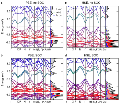
Electronic structure: The electronic band structures and density of states (DOS) of \ceCuInTe2 as calculated with the PBE functional with SOC both included and not included are shown in Figure 2a-b. The orbital-resolved DOS reveals the valence band to be mainly Cu 3d and Te 5p character, while the conduction band contains a fraction of In 5s states, as shown in the orbital projections in Figure 2. With SOC not included, at there are two doubly-degenerate bands at the Fermi level and two doubly-degenerate bands very close to the Fermi level, as shown in Figure 3a. The effect of SOC is to lift these degeneracies and introduce further spin splitting throughout the band structure. In addition, the band gap (Eg) with PBE, which is zero when SOC is not included, is opened to 6 meV with SOC. This is more clearly seen in Figure 3a-b, which shows the band structure magnified around the Fermi level at and projected onto the different spin channels. For the band structures without SOC included, the spin-up and spin-down channels are degenerate. When SOC is included, the spin projection onto the x-direction reveals the degeneracy to be lifted by spin component. This Dresselhaus spin splitting results from the lack of inversion symmetry in the structure of \ceCuInTe2 and presence of spin-orbit coupling. In fact, the Dresselhaus effect was originally proposed for zinc blende structures from which the chalcopyrite structure of \ceCuInTe2 is derived.Dresselhaus (1955)
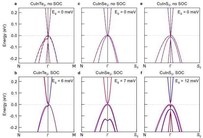
For the \ceCuInSe2 and \ceCuInS2 structures, Eg is also zero when SOC is not included, and Eg is opened to 7 meV and 12 meV respectively when SOC is included, also shown in Figure 3. Different band structure paths are shown due to the position of the valence band maximum (VBM) and conduction band minimum (CBM): for \ceCuInTe2 with SOC, the VBM and CBM are slightly away from in the M direction, whereas \ceCuInSe2 and \ceCuInS2 have the VBM along and the CBM at with no SOC, and the VBM along N and the CBM at with SOC included. Contrary to what is expected for SOC-mediated band inversion where heavier ions would result in greater Eg, here we find that Eg decreases with increasing anion mass (SSeTe). In this case, the Eg differences are a result of higher energy p-orbitals hybridizing more strongly with metal d-orbitals and forming a more disperse valence band. Furthermore there is no evidence of band inversion seen in the orbital projections on the bands given in SI Figure 1. However, the enhanced spin-splitting effect is clearly seen in the spin-projected bands (Figure 3) and in comparison of the full band structures of the materials series (SI Figure 1).
The generalized gradient approximation on which the PBE functional is based is well-known to underestimate band gaps. Therefore, the band structures were also calculated with the hybrid functional HSE06, which has been shown to perform better for Eg in semiconductors.Krukau et al. (2006) Eg of \ceCuInTe2 is opened to 0.74 eV without SOC, and the effect of SOC is much larger - reducing Eg to 0.54 eV as shown in Figure 2c-d. The band gaps of \ceCuInSe2 and \ceCuInS2 without (and with) SOC included are 0.62 eV (0.56 eV) and 1.08 eV (1.08 eV) respectively. The differences in band gaps show the diminishing effect of SOC through the series as lighter elements have smaller relativistic effects.Herman et al. (1963) This can also be seen in the reduction in spin-splitting across the band structures calculated with HSE06, which are given in SI Figure 2.
III.1.2 Tin pnictides
Structural details: Next we turn to \ceSrSn2As2, shown in Figure 1b, which belongs to the tin pnictide family (space group Rm, number 166). The crystal structure consists of layers of edge-sharing \ceSrAs6 octahedra alternating with layers of Sn. The tin pnictides recently gained interest when \ceNaSn2As2 and Na1-xSn2P2 were found to be superconductors with TC 1.3 K and 2.0 K respectively.Goto et al. (2017, 2018) Unlike the exotic superconductivity present in the stoichiometrically similar Fe-pnictide compounds (e.g. BaFe2As2) with the Fmmm space group, \ceNaSn2As2 has been classified as a phonon-mediated conventional superconductor.Ishihara et al. (2018)
The tin pnictides are also isostructural to the topological insulator \ceBi2Te2Se, consisting of layers of \ceSeBi6 octahedra alternating with layers of Te.Xiong et al. (2012); Bland and Basinski (1961) \ceSrSn2As2 itself has been theoretically predicted to be an enforced 3D-Dirac semimetal lying naturally close to the topological critical point.Gibson et al. (2015) Experimental evidence of a topological insulating state in \ceSrSn2As2 from angle-resolved photoemission spectroscopy has been reported by Rong et al., although interpretation of these results was not clear-cut and the band gap of the structure was not measured.Rong et al. (2017) They also note from their DFT calculations that the topological state was sensitive to the choice of exchange-correlation functional.
To investigate the role of SOC and ion sizes, we fully substituted isovalent ions on both the Sr and As sites. For the Sr site, we considered other alkali earth metals with \ceMgSn2As2, \ceCaSn2As2 and \ceBaSn2As2. For the As site we substituted in P, resulting in \ceSrSn2P2. The optimized calculated lattice parameters are compared to experimental values in SI Table 3. There are limited measurements of the lattice parameters reported for these compounds, and in some cases we have estimated the lattice parameter by extrapolating from the available experimental lattice parameters of mixed cation compounds according to Vegard’s law. Taking this into consideration, the calculated lattice parameters compare favourably with reported structures.Asbrand et al. (1995) Both lattice parameters a and c increase with increasing cation mass (MgCaSrBa) and anion mass (PAs).
| Eg PBE (eV) | Eg HSE06 (eV) | |||
| Material | Without SOC | With SOC | Without SOC | With SOC |
| \ceMgSn2As2 | 0 | 0 | – | – |
| \ceCaSn2As2 | 0 | 0 | 0 | 0 |
| \ceSrSn2As2 | 0 | 0.057 | 0.029 | 0.070 |
| \ceBaSn2As2 | 0 | 0.054 | 0.049 | 0.112 |
| \ceSrSn2P2 | 0.028 | 0.016 | 0.181 | 0.198 |
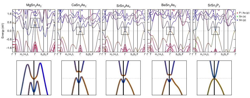
Electronic structure: The calculated PBE+SOC orbital projected band structures are shown in Figure 4. All four of the As-compounds exhibit band inversion at the high-symmetry point with avoided band-crossings appearing at several places across all five band structures. This indicates a strong degree of spin-orbit interaction, as many of these avoided crossings are not observed, or occur to a lesser degree, in the band structures calculated without SOC (see SI Figure 3). Calculated band gaps are shown in Table 1, with \ceMgSn2As2 and \ceCaSn2As2 being metallic, \ceSrSn2As2 and \ceBaSn2As2 having a small and indirect band gap, and \ceSrSn2P2 having a small and direct band gap with PBE. The trend in Eg with ion mass PAs is reversed when SOC is or is not included suggesting that Eg is strongly dependent on SOC in this structure.
The compounds \ceCaSn2As2, \ceSrSn2As2, \ceBaSn2As2 and \ceSrSn2P2 were further investigated by calculations with HSE06. The band gaps are given in Table 1 and the HSE06+SOC band structures in SI Figure 4. Aside from \ceCaSn2As2, which remains a semimetal, we find that with HSE06 the band gap opens up, and when including SOC the band gap opens further. This latter effect is greatest in \ceBaSn2As2, which contains the heaviest elements, then \ceSrSn2As2, and finally \ceSrSn2P2, the lightest compound considered. Despite this, the band gaps calculated by HSE06+SOC remain at the meV order of magnitude.
Finally, we address the qualitative difference between the band structures at the Fermi level between \ceMgSn2As2 and the other tin pnictide compounds considered. The orbital-resolved DOS of \ceSrSn2As2 and \ceMgSn2As2, shown in SI Figure 5, reveals states near the top of the valence band and near the bottom of the conduction band to have a mixture of mainly As 4p, Sn 5s and Sn 5p character. This indicates hybridization between Sn and As orbitals within the SnAs bilayers, as is also reported in other tin arsenide layered compounds.Arguilla et al. (2016, 2017) However, in the Mg case, there are also Mg s states at the Fermi level, which cause a spectral weight redistribution resulting in a much greater DOS at the Fermi level, and a shift upwards of the nodal crossing.
| Without SOC | With SOC | ||
| Material | Classification | Position | Classification |
| \ceMgSn2As2 | HSLSM | F-S- | TI |
| \ceCaSn2As2 | HSLSM | F-S- | TI |
| \ceSrSn2As2 | HSLSM | F-S- | TI |
| \ceBaSn2As2 | HSLSM | F-S- | TI |
| \ceSrSn2P2 | Trivial | – | Trivial |
Topological characterization: As the tin pnictides studied here are charge-balanced, the Dirac point is symmetry allowed but dependent on the energy levels and band dispersions.Gibson et al. (2015) Hence, the critical point varies with the constituent elements and the calculation parameters. With the PBE+SOC level of theory, the band inversion resulting in indirect band gaps of \ceSrSn2As2 and \ceBaSn2As2 suggest they are topologically nontrivial, whereas the direct band gap without band inversion of \ceSrSn2P2 suggests it to be a trivial insulator. We screen the topological properties of the five candidate pnictides using the symtopo package which calculates the compatibility conditions of the band representations along high symmetry lines in the Brillouin zone (BZ).He et al. (2019) Violations of these conditions indicates a symmetry-protected crossing which is then labelled with the crossing’s position in the BZ. Finally, for gapped cases, symmetry-based indicators are used to distinguish topological insulators and topological crystalline insulators. We summarize our results of topological classification in Table 2 both with and without SOC. We find all of the Sn-As compounds to be high-symmetry-line semimetals (HSLSMs) without SOC, with the crossing occurring along the F-S- high-symmetry line. Including SOC causes the HSLSM to gap out and result in a topological insulator (TI). However, for \ceSrSn2P2, both cases with and without SOC result in a trivial phase.
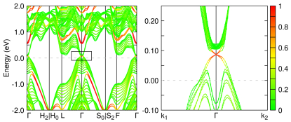
We further investigate the topological properties of a representative Sn-As compound, \ceSrSn2As2, by calculating the topological invariants and surface states with WannierTools. We confirm the nontrivial topology by calculating the topological invariant Z2. For \ceSrSn2As2 with PBE+SOC, (v0;v1v2v3) is (1;000) indicating a strong topological insulator. Furthermore, the calculated surface band structure shown in Figure 5 reveals a surface Dirac cone in the bulk band gap at . We also observe some bending of the surface bands, which is unsurprising due to the small band gap.
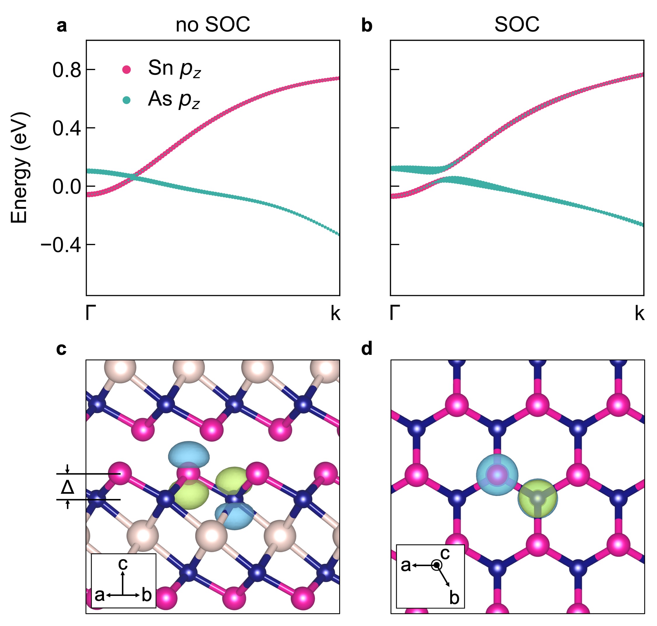
We further analyze a detail of the \ceSrSn2As2 band structure at a SOC-mediated gap opening close to and near in Figure 6 to elucidate the origins of the critical point. Orbital decomposition of the bands reveals that one is composed of mostly Sn states and the other of As states. Without SOC (Figure 6a), the bands cross resulting in a Dirac point, whereas when SOC is included (Figure 6b), the bands hybridize, exchange character and a gap opens. Wannier functions of the corresponding Sn and As orbitals, shown in Figure 6c, reveal that the orbitals align perpendicular to the layers of the structure. A top down view reveals a honeycomb structure within the Sn–As bilayer, Figure 6d, which provides the symmetry protection for the Dirac crossing, as in the Kane—Mele model.Kane and Mele (2005) Buckling of the bilayer allows overlap between the bonds despite the long Sn–As bond length compared to graphene. As the cation size decreases from Ba to Mg, the buckling of the Sn–As bilayer increases, with a corresponding increase in bilayer height ( indicated in Figure 6c). We find that the bilayer height has a linear relationship with the group velocity at the band crossing shown in Figure 6a, ranging from 3.7 eVÅ in \ceBaSn2As2 to 5.1 eVÅ in \ceMgSn2As2 (SI Table 4).
All three compounds \ceSrSn2As2, \ceBaSn2As2 and \ceSrSn2P2 are trivial insulators when calculated by HSE06+SOC, as the hybrid functional unwinds the bands past the critical point and the band gap opens up. The dependency of topological order on choice of functional indicates that these compounds lie naturally close to the critical point. This suggests the possibility of tuning the topological order by other degrees of freedom such as strain. For example, as we vary the composition CaSrBa the HSE06 band gap increases and this coincides with increasing Sn–As bond length. Therefore, the band structure, and hence band gap, can be manipulated towards the critical point by reducing the interlayer distance with a compressive strain.
III.1.3 \ceLi6Bi2O7
Structural details: The structure of \ceLi6Bi2O7 in the Materials Project databasePersson (2016) is in the space group P21/c (number 14) and consists of \ceBiO6 octahedra that are both corner- and edge-sharing (shown in Figure 1c). Li resides in channels between these octahedra. However, this compound has not been reported by experiment. Upon closer inspection of the composition, we note that the stoichiometry corresponds to Bi being in the +4 oxidation state, although Bi+4 is unstable against disproportionation into Bi+3 and Bi+5 ions.Mazin et al. (1995) Accordingly, a charge-ordered Li6Bi+3Bi+5O7 structure is expected, which would manifest in a difference in bonding on two Bi sites.Cox and Sleight (1976) The P21/c structure does not capture this, having equivalent bond lengths on every Bi site, with average Bi–O bond length , and equal polyhedral volumes of 14.90 Å3. We therefore predict that the compound will not exist in the structure given in the database. However, we here examine the given structure and will address the possibility of a lower symmetry, charge-ordered structure in a following work.
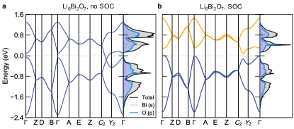
Electronic structure: The data set from which the materials were selected predicted that a band gap opened when spin-orbit coupling was included with the PBE functional. However, our PBE calculations which were performed with the converged set of parameters given in SI Table 1 predict the material to be metallic both with and without SOC. When the hybrid functional HSE06 is used, however, a spin-orbit gap does open up. Figure 7a shows the electronic band structure and orbital-resolved density of states calculated with HSE06 when SOC is not included, showing band crossing just below the Fermi level. Including SOC, Figure 7b shows a degree of spin splitting and separation of the valence and conduction bands resulting in an indirect band gap of 78 meV. The density of states has a majority O 2p and Bi 6s character in the region around the Fermi level, indicating that the electronic properties are determined by the hybridization between these two orbitals with the SOC-driven gap resulting from the heavy Bi ion. We conclude that this hypothetical structure indeed fulfils the criteria of a spin-orbit gapped semiconductor, but will not be stable in nature.
III.2 Suitability as Dark Matter Targets
The indium chalcogenide compounds \ceCuInTe2, \ceCuInSe2 and \ceCuInS2 have SOC-induced small band gaps under the generalized gradient approximation. However, the larger band gap predicted by hybrid functionals is in better agreement with the experimentally measured values, as expected for regular semiconductors.Frick et al. (2018); Neumann (1986); Yoshino et al. (2001) Including SOC worsens the prediction of Eg in comparison to experiment (\ceCuInTe2 has an optical band gap of 0.9 eV; HSE06 predicts 0.74 eV without SOC and 0.54 eV with SOC), but the effects are needed to reveal features of the experimentally measured band structure such as splitting of the valence band.Frick et al. (2018); Neumann (1986) Regardless, the band gaps of the compounds have been comprehensively determined by experiment, and, being of the order of an eV, are too large for our desired absorption of DM with meV masses or scattering of DM with keV masses.
The tin pnictides have an electronic structure that is strongly influenced by SOC due to the topological nature of the compounds. At the PBE level of theory, the structures exhibited band inversion such that even when the hybrid functional was used, the band gaps opened up as expected but remained at the meV scale. With this change in functional, \ceSrSn2As2 and \ceBaSn2As2 pass through the topological critical point, resulting in direct band gaps of 70 and 112 meV respectively. \ceSrSn2P2 is a trivial insulator in both cases, and the change in functional causes a larger gap opening to 198 meV. These three materials can offer improved sensitivity to light dark matter interactions over traditional semiconducting compounds with eV scale band gaps. The 70-200 meV range predicted by HSE06 provides multiple options for precisely targeted and tunable light DM masses. Additionally, as the composition is varied by changing the cation, the Sn–As bilayer height is modulated which has the effect of also tuning the group velocity. For \ceCaSn2As2, \ceSrSn2As2 and \ceBaSn2As2, this band crossing is close to the Fermi level, such that the Fermi velocity () is varied from 4.3 to 3.7 eVÅ. To maximize the DM-scattering rate, should be the same as the velocity of DM, which is .Hochberg et al. (2018) The tin pnictides are close to an ideal match: \ceCaSn2As2 = , \ceSrSn2As2 = , \ceBaSn2As2 = . These values are comparable to \ceZrTe5 ( = , = , = ) which provides an excellent DM reach.Hochberg et al. (2018) Like \ceZrTe5, the tin pnictides also have anisotropic velocities, which will enable directional detection for capturing daily or annual modulation of a DM signal, distinguishing it uniquely from background signals. For example, the group velocities vary by two orders of magnitude: = and = for \ceSrSn2As2.
The band gap and Fermi velocity of the target material determine the lower bound of the mass sensitivity and its cross section with DM respectively. Anisotropic Fermi velocities can provide directional targets whereby the incoming DM wind gives a directional dependence – the ‘smoking gun’ of DM detection. Therefore, being able to tune these two critical parameters within one family of materials offers substantial benefits for the design of detection experiments. Furthermore, there is the possibility to expand this range further than considered here by varying the composition through different combinations of cation and pnictogen. Crucially, solid solutions have already been experimentally realized, and mixtures on either cation or anion sites could provide fine tuning of the band gap.Asbrand et al. (1995) In fact, for certain DM interactions a direct band gap is preferred over an indirect band gap, as the higher probability of a direct excitation improves the target sensitivity.
The \ceLi6Bi2O7 compound also has an meV scale band gap predicted by HSE06+SOC, however the structure examined here is likely to be unstable and any symmetry lowering is likely to affect the band gap. More specifically, charge disproportionation is likely to lead to a lowering of the symmetry of the structure, leading to a reduction in orbital overlap and increase of the band gap. This compound has not been reported previously, and there are no experimental measurements available.
III.3 Theoretical Predictions of Spin-Orbit Gapped Materials
The analysis presented here highlights some of the drawbacks of a DFT-based search for low band gap materials. Of the three materials families which had a spin-orbit gap predicted by PBE, two did not maintain meV-scale band gaps under closer investigation. Some of these shortcomings have been discussed previously in relation to predicted topological materials,Vidal et al. (2011); Vergniory et al. (2013); Zunger (2019); Malyi et al. (2020) however there is no one method that will give reliable predictions in all cases.
The most important consideration for detector applications is the structural stability, and hence experimental realization of the predicted target. If a compound has not previously been synthesized, then its thermodynamic stability can be estimated by phonon analysis or energy above the convex hull, if necessary identifying competing phases using structure prediction tools. In the case of \ceLi6Bi2O7, even though a stable energy above hull was predictedPersson (2016) (within calculation error), the insufficient treatment of charge localization by PBE failed to capture a structural distortion stemming from charge disproportionation. While the prediction of experimentally unfeasible structures is not unique to the field of topological materials, the symmetry requirements of non-trivial topology mean that any symmetry-breaking structural changes can invalidate a topological analysis. More generally, the close structure-property relationship of spin-orbit band gaps implies that even small changes in geometry will have a large effect.
A second drawback of DFT-led searches for low band gap materials is the underestimation of trivial band gaps by standard DFT approximations; this has the opposite effect of overestimation of gaps with band inversion, which can lead to false positive topological materials and incorrect band dispersions.An et al. (2014); Förster et al. (2015, 2016) This has remained a caveat for high-throughput computational searches of topological insulators.Yang et al. (2012); Olsen et al. (2019) Going beyond DFT, the GW approximation is the most accurate method for predicting electronic properties without parameterization, improving upon both the bulk and surface electronic structure of topological insulators and giving results consistent with experimental photoemission, optical and EELS spectra.Aguilera et al. (2015, 2019) However, quasiparticle self-consistent GW (QSGW) is known to systematically overestimate band gaps,Svane et al. (2011) which can lead to false negative topological classifications of small band gap materials. Furthermore, given the many variations of GW available, electronic properties are sensitive to computational choices such as the number of self-consistent steps, whether SOC is included directly or as a perturbation, and the ad-hoc correction of the hybrid QSGW scheme. These can cause gap variations greater than 1 eV.Garza and Scuseria (2016) For materials close to the topological critical point, these choices can result in qualitatively different topological classifications.Svane et al. (2011); Aguilera et al. (2013a, b)
Importantly, depending on the system size and properties of interest, calculations with GW approximations can be prohibitively expensive. The hybrid density functionals, which eliminate much of the self-interaction error of DFT by including a fraction of exact Hartree-Fock exchange, have been extremely successful as a mid-cost level of theory that can give GW-quality results for topological materials.Vidal et al. (2011); Crowley et al. (2015); Malyi et al. (2020) However, the screened hybrid functionals, such as the HSE06 functional used here, rely on fixed parameters for screening length and percentage of exact exchange, and predicted band gaps are dependent on these parameters. A single hybrid functional with a fixed amount of exact exchange cannot accurately describe small and large band gap materials simultaneously, and the settings that have been benchmarked for general use will tend to overestimate the band gaps of narrow-gapped materials.Garza and Scuseria (2016) In topological insulators, this could lead to underestimations of inverted band gaps and false negative topological classifications. Therefore, if parameterization via experimental results is not possible, hybrid functionals are not necessarily more accurate than PBE.Li et al. (2014) In the case of the topological semimetal GaGeTe, HSE overestimated the band gap and predicted a trivial gap, whilst PBE gave a closer match to the measured band gap and supported the topological classification from experiment, although the nature of the indirect gap was not captured by either HSE or PBE.Haubold et al. (2019) The family of tin pnictides shown here is one example of a topological classification that is dependent on the choice of PBE or hybrid exchange correlation functional, and there are other examples in literature.Vidal et al. (2011); Sun et al. (2011) Aside from the treatment of charge localization, even small differences in geometry from different functionals can affect the topological classification.Reid et al. (2020) In these edge cases, careful consideration of the electronic structure can be taken on a case-by-case basis, however, experimental verification is always necessary.
Conclusions
Three materials, \ceCuInTe2, \ceSrSn2As2 and \ceLi6Bi2O7, predicted by DFT to have band gaps induced by spin-orbit coupling interactions, were investigated for their electronic and topological properties. These materials and a range of isostructural compounds were evaluated for their suitability as low-mass dark matter detection targets.
The band gaps of \ceCuInTe2, \ceCuInSe2 and \ceCuInS2 predicted by HSE06+SOC were found to be in good agreement with experiment, but are too large to be sensitive to light dark matter. Likewise with \ceLi6Bi2O7, using HSE06+SOC led to an increased prediction of the band gap compared to PBE, but structural distortions associated with charge disproportionation must be further investigated, and synthesis routes explored.
The family of tin pnictides, however, has several properties making them promising as targets for light DM detection. Firstly, direct band gaps ranging from 70-200 meV are predicted across the three compounds \ceSrSn2As2, \ceBaSn2As2 and \ceSrSn2P2 and can be tuned by alloying, making them sensitive to sub-GeV DM candidates. Secondly, the tunable Fermi velocity suggests that these compounds can be kinematically matched with DM to optimize the cross section between DM and electrons in the target, additionally providing a route for directional direction. Finally, some of the family have already been synthesized in crystal form and found to lie close to a topological critical point. However, further experimental studies are needed to fully characterize the structure-property phase space in addition to further variations on composition for tuning of the band gap both within and beyond the range presented here.
Acknowledgements
We thank Anubhav Jain for discussions and help generating the spin-orbit coupling data set used by this work. We also thank Junsoo Park for helpful discussions regarding Wannier functions. S.G. and K.I. were supported by the Laboratory Directed Research and Development Program of LBNL under the U.S. Department of Energy (DoE) Contract No. DE-AC02-05CH11231. Computational resources were provided by the National Energy Research Scientific Computing Center and the Molecular Foundry, DoE Office of Science User Facilities supported by the Office of Science of the U.S. Department of Energy under Contract No. DE-AC02-05CH11231. The work performed at the Molecular Foundry was supported by the Office of Science, Office of Basic Energy Sciences, of the U.S. Department of Energy under the same contract. A.F. was funded by the DOE Basic Energy Sciences program—the Materials Project—under Grant No. KC23MP.
References
- Battaglieri et al. (2017) M. Battaglieri, A. Belloni, A. Chou, P. Cushman, B. Echenard, R. Essig, J. Estrada, J. L. Feng, B. Flaugher, P. J. Fox, et al., US Cosmic Visions: New Ideas in Dark Matter 2017: Community Report, Tech. Rep. (2017).
- Derenzo et al. (2017) S. Derenzo, R. Essig, A. Massari, A. Soto, and T.-T. Yu, Physical Review D 96, 016026 (2017).
- Hochberg et al. (2018) Y. Hochberg, Y. Kahn, M. Lisanti, K. M. Zurek, A. G. Grushin, R. Ilan, S. M. Griffin, Z. F. Liu, S. F. Weber, and J. B. Neaton, Physical Review D 97, 015004 (2018).
- Hochberg et al. (2016a) Y. Hochberg, M. Pyle, Y. Zhao, and K. M. Zurek, Journal of High Energy Physics 57 (2016a).
- Hochberg et al. (2016b) Y. Hochberg, T. Lin, and K. M. Zurek, Physical Review D 94, 015019 (2016b).
- Knapen et al. (2018) S. Knapen, T. Lin, M. Pyle, and K. M. Zurek, Physics Letters B 785, 386 (2018).
- Knapen et al. (2017) S. Knapen, T. Lin, and K. M. Zurek, Physical Review D 95, 056019 (2017).
- Trickle et al. (2020) T. Trickle, Z. Zhang, K. M. Zurek, K. Inzani, and S. M. Griffin, Journal of High Energy Physics 2020, 36 (2020), arXiv:1910.08092 .
- Griffin et al. (2020) S. M. Griffin, K. Inzani, T. Trickle, Z. Zhang, and K. M. Zurek, Physical Review D 101, 055004 (2020), arXiv:1910.10716 .
- Hochberg et al. (2017) Y. Hochberg, T. Lin, and K. M. Zurek, Physical Review D 95, 023013 (2017).
- Essig et al. (2016) R. Essig, M. Fernandez-Serra, J. Mardon, A. Soto, T. Volansky, and T.-T. Yu, Journal of High Energy Physics 46 (2016).
- Baker (2017) I. M. Baker, in II-VI Narrow Bandgap Semiconductors: Optoelectronics, Springer Handbook of Electronic and Photonic Materials (Springer International Publishing, Cham, 2017).
- Shi et al. (2016) X. Shi, L. Chen, and C. Uher, International Materials Reviews 61, 379 (2016).
- Geilhufe et al. (2018) R. M. Geilhufe, B. Olsthoorn, A. D. Ferella, T. Koski, F. Kahlhoefer, J. Conrad, and A. V. Balatsky, Physica Status Solidi (RRL)–Rapid Research Letters 12, 1800293 (2018).
- Geilhufe et al. (2020) R. M. Geilhufe, F. Kahlhoefer, and M. W. Winkler, Physical Review D 101, 055005 (2020).
- Sánchez-Martínez et al. (2019) M.-Á. Sánchez-Martínez, I. Robredo, A. Bidaurrazaga, A. Bergara, F. de Juan, A. G. Grushin, and M. G. Vergniory, Journal of Physics: Materials 3, 014001 (2019).
- Nair et al. (2018) N. L. Nair, P. T. Dumitrescu, S. Channa, S. M. Griffin, J. B. Neaton, A. C. Potter, and J. G. Analytis, Physical Review B 97, 041111 (2018).
- Xu et al. (2018) B. Xu, L. X. Zhao, P. Marsik, E. Sheveleva, F. Lyzwa, Y. M. Dai, G. F. Chen, X. G. Qiu, and C. Bernhard, Phys. Rev. Lett. 121, 187401 (2018).
- Monserrat and Narayan (2019) B. Monserrat and A. Narayan, Phys. Rev. Research 1, 033181 (2019).
- Perdew and Levy (1983) J. P. Perdew and M. Levy, Physical Review Letters 51, 1884 (1983).
- Perdew (1986) J. P. Perdew, International Journal of Quantum Chemistry: Quantum Chemistry Symposium 19, 497 (1986).
- Mori-Sánchez et al. (2008) P. Mori-Sánchez, A. J. Cohen, and W. Yang, Physical Review Letters 100 (2008).
- Krukau et al. (2006) A. V. Krukau, O. A. Vydrov, A. F. Izmaylov, and G. E. Scuseria, The Journal of Chemical Physics 125, 224106 (2006).
- Garza and Scuseria (2016) A. J. Garza and G. E. Scuseria, Journal of Physical Chemistry Letters 7, 4165 (2016), arXiv:1608.04796 .
- Crowley et al. (2016) J. M. Crowley, J. Tahir-Kheli, and W. A. Goddard, Journal of Physical Chemistry Letters 7, 1198 (2016).
- Kresse and Hafner (1993) G. Kresse and J. Hafner, Physical Review B 47, 558 (1993).
- Kresse and Hafner (1994) G. Kresse and J. Hafner, Physical Review B 49, 14251 (1994).
- Kresse and Furthmüller (1996a) G. Kresse and J. Furthmüller, Computational Materials Science 6, 15 (1996a).
- Kresse and Furthmüller (1996b) G. Kresse and J. Furthmüller, Physical Review B 54, 11169 (1996b).
- Blöchl (1994) P. Blöchl, Physical Review B 50, 17953 (1994).
- Kresse and Joubert (1999) G. Kresse and D. Joubert, Physical Review B 59, 1758 (1999).
- Perdew et al. (1996) J. P. Perdew, K. Burke, and M. Ernzerhof, Physical Review Letters 77, 3865 (1996).
- Heyd et al. (2003) J. Heyd, G. E. Scuseria, and M. Ernzerhof, Journal of Chemical Physics 118, 8207 (2003).
- Heyd et al. (2006) J. Heyd, G. E. Scuseria, and M. Ernzerhof, Journal of Chemical Physics 124 (2006).
- Steiner et al. (2016) S. Steiner, S. Khmelevskyi, M. Marsmann, and G. Kresse, Physical Review B 93, 224425 (2016).
- M Ganose et al. (2018) A. M Ganose, A. J Jackson, and D. O Scanlon, Journal of Open Source Software 3, 717 (2018).
- He et al. (2019) Y. He, Y. Jiang, T. Zhang, H. Huang, C. Fang, and Z. Jin, Chinese Physics B 28, 087102 (2019).
- Wu et al. (2018) Q. Wu, S. Zhang, H.-F. Song, M. Troyer, and A. A. Soluyanov, Computer Physics Communications 224, 405 (2018).
- Pizzi et al. (2020) G. Pizzi, V. Vitale, R. Arita, S. Blügel, F. Freimuth, G. Géranton, M. Gibertini, D. Gresch, C. Johnson, T. Koretsune, et al., Journal of Physics: Condensed Matter 32, 165902 (2020).
- pri (2019) “Private correspondance with Anubhav Jain.” (2019).
- Herman et al. (1963) F. Herman, C. D. Kuglin, K. F. Cuff, and R. L. Kortum, Physical Review Letters 11, 541 (1963).
- Rincón and Ramírez (1992) C. Rincón and F. J. Ramírez, Journal of Applied Physics 72, 4321 (1992).
- Hwang et al. (1978) H. Hwang, C. Sun, C. Leu, C. Cheng, and C. Tu, Revue de Physique Appliquée 13, 745 (1978).
- Kazmerski and Shieh (1977) L. L. Kazmerski and C. C. Shieh, Thin Solid Films 41, 35 (1977).
- Neumann (1986) H. Neumann, Solar Cells 16, 317 (1986).
- Rockett and Birkmire (1991) A. Rockett and R. W. Birkmire, Journal of Applied Physics 70, R81 (1991).
- Yoshino et al. (2001) K. Yoshino, T. Ikari, S. Shirakata, H. Miyake, and K. Hiramatsu, Applied Physics Letters 78, 742 (2001).
- Bi et al. (2012) W. Bi, M. Zhou, Z. Ma, H. Zhang, J. Yu, and Y. Xie, Chemical Communications 48, 9162 (2012).
- Frick et al. (2018) J. J. Frick, A. Topp, S. Klemenz, M. Krivenkov, A. Varykhalov, C. R. Ast, A. B. Bocarsly, and L. M. Schoop, The Journal of Physical Chemistry Letters 9, 6833 (2018).
- Liu et al. (2012) R. Liu, L. Xi, H. Liu, X. Shi, R. Liu, and L. Chen, Chemical Communications 48, 3818 (2012).
- Dresselhaus (1955) G. Dresselhaus, Physical Review 100, 580 (1955).
- Goto et al. (2017) Y. Goto, A. Yamada, T. D. Matsuda, Y. Aoki, and Y. Mizuguchi, Journal of the Physical Society of Japan 86, 19 (2017).
- Goto et al. (2018) Y. Goto, A. Miura, C. Moriyoshi, Y. Kuroiwa, T. D. Matsuda, Y. Aoki, and Y. Mizuguchi, Scientific Reports 8, 12852 (2018).
- Ishihara et al. (2018) K. Ishihara, T. Takenaka, Y. Miao, O. Tanaka, Y. Mizukami, H. Usui, K. Kuroki, M. Konczykowski, Y. Goto, Y. Mizuguchi, and T. Shibauchi, Physical Review B 98, 1 (2018).
- Xiong et al. (2012) J. Xiong, A. Petersen, D. Qu, Y. Hor, R. Cava, and N. Ong, Physica E: Low-dimensional Systems and Nanostructures 44, 917 (2012).
- Bland and Basinski (1961) J. A. Bland and S. J. Basinski, Canadian Journal of Physics 39, 1040 (1961).
- Gibson et al. (2015) Q. D. Gibson, L. M. Schoop, L. Muechler, L. S. Xie, M. Hirschberger, N. P. Ong, R. Car, and R. J. Cava, Physical Review B 91, 205128 (2015).
- Rong et al. (2017) L.-Y. Rong, J.-Z. Ma, S.-M. Nie, Z.-P. Lin, Z.-L. Li, B.-B. Fu, L.-Y. Kong, X.-Z. Zhang, Y.-B. Huang, H.-M. Weng, T. Qian, H. Ding, and R.-Z. Tai, Scientific Reports 7, 6133 (2017).
- Asbrand et al. (1995) M. Asbrand, B. Eisenmann, and J. Klein, Zeitschrift für anorganische und allgemeine Chemie 621, 576 (1995).
- Arguilla et al. (2016) M. Q. Arguilla, J. Katoch, K. Krymowski, N. D. Cultrara, J. Xu, X. Xi, A. Hanks, S. Jiang, R. D. Ross, R. J. Koch, S. Ulstrup, A. Bostwick, C. Jozwiak, D. W. McComb, E. Rotenberg, J. Shan, W. Windl, R. K. Kawakami, and J. E. Goldberger, ACS Nano 10, 9500 (2016).
- Arguilla et al. (2017) M. Q. Arguilla, N. D. Cultrara, Z. J. Baum, S. Jiang, R. D. Ross, and J. E. Goldberger, Inorganic Chemistry Frontiers 4, 378 (2017).
- Kane and Mele (2005) C. L. Kane and E. J. Mele, Physical Review Letters 95, 1 (2005), arXiv:0411737 [cond-mat] .
- Persson (2016) K. Persson, “Materials Data on Li6Bi2O7 (SG:14) by Materials Project,” (2016).
- Mazin et al. (1995) I. I. Mazin, A. I. Liechtenstein, and O. V. Ivanov, Ferroelectrics 164, 169 (1995).
- Cox and Sleight (1976) D. Cox and A. Sleight, Solid State Communications 19, 969 (1976).
- Vidal et al. (2011) J. Vidal, X. Zhang, L. Yu, J. W. Luo, and A. Zunger, Physical Review B - Condensed Matter and Materials Physics 84, 1 (2011).
- Vergniory et al. (2013) M. G. Vergniory, M. A. Marques, S. Botti, M. Amsler, S. Goedecker, E. V. Chulkov, A. Ernst, and A. H. Romero, Physical Review Letters 110, 129701 (2013).
- Zunger (2019) A. Zunger, Nature 566, 447 (2019).
- Malyi et al. (2020) O. I. Malyi, G. M. Dalpian, X. G. Zhao, Z. Wang, and A. Zunger, Materials Today 32, 35 (2020), arXiv:1812.10573 .
- An et al. (2014) W. An, F. Wu, H. Jiang, G.-S. Tian, and X.-Z. Li, The Journal of Chemical Physics 141, 084701 (2014).
- Förster et al. (2015) T. Förster, P. Krüger, and M. Rohlfing, Physical Review B 92, 201404 (2015).
- Förster et al. (2016) T. Förster, P. Krüger, and M. Rohlfing, Physical Review B 93, 205442 (2016).
- Yang et al. (2012) K. Yang, W. Setyawan, S. Wang, M. Buongiorno Nardelli, and S. Curtarolo, Nature Materials 11, 614 (2012).
- Olsen et al. (2019) T. Olsen, E. Andersen, T. Okugawa, D. Torelli, T. Deilmann, and K. S. Thygesen, Physical Review Materials 3, 1 (2019).
- Aguilera et al. (2015) I. Aguilera, I. A. Nechaev, C. Friedrich, S. Blügel, and E. V. Chulkov, in Many-Body Effects in the Electronic Structure of Topological Insulators, Topological Insulators (Wiley-VCH Verlag GmbH & Co. KGaA, Weinheim, Germany, 2015) pp. 161–189.
- Aguilera et al. (2019) I. Aguilera, C. Friedrich, and S. Blügel, Physical Review B 100, 155147 (2019).
- Svane et al. (2011) A. Svane, N. E. Christensen, M. Cardona, A. N. Chantis, M. Van Schilfgaarde, and T. Kotani, Physical Review B - Condensed Matter and Materials Physics 84, 1 (2011).
- Aguilera et al. (2013a) I. Aguilera, C. Friedrich, and S. Blügel, Physical Review B 88, 165136 (2013a).
- Aguilera et al. (2013b) I. Aguilera, C. Friedrich, G. Bihlmayer, and S. Blügel, Physical Review B 88, 045206 (2013b).
- Crowley et al. (2015) J. M. Crowley, J. Tahir-Kheli, and W. A. Goddard, Journal of Physical Chemistry Letters 6, 3792 (2015).
- Li et al. (2014) C. Li, T. Winzer, A. Walsh, B. Yan, C. Stampfl, and A. Soon, Physical Review B 90, 075438 (2014), arXiv:1408.5188 .
- Haubold et al. (2019) E. Haubold, A. Fedorov, F. Pielnhofer, I. P. Rusinov, T. V. Menshchikova, V. Duppel, D. Friedrich, R. Weihrich, A. Pfitzner, A. Zeugner, A. Isaeva, S. Thirupathaiah, Y. Kushnirenko, E. Rienks, T. Kim, E. V. Chulkov, B. Büchner, and S. Borisenko, APL Materials 7 (2019).
- Sun et al. (2011) Y. Sun, X. Q. Chen, C. Franchini, D. Li, S. Yunoki, Y. Li, and Z. Fang, Physical Review B - Condensed Matter and Materials Physics 84, 1 (2011), arXiv:1105.5841 .
- Reid et al. (2020) T. K. Reid, S. Pamir Alpay, A. V. Balatsky, and S. K. Nayak, Physical Review B 101, 1 (2020).