Hyper Resolution Two Photon Direct Laser Writing using ENZ Nano-Cavity
Abstract
A novel technique is reported to improve the resolution of two-photon direct laser writing lithography. Thanks to the high collimation enabled by extraordinary (near-zero) metamaterial features, ultra-thin dielectric hyper resolute nanostructures are within reach. With respect to the standard direct laser writing approach, a size reduction of and , in height and width respectively, is achieved with the height of the structures adjustable between 5nm and 50nm. The retrieved 2D fabrication parameters are exploited for fabricating hyper resolute 3D structures. In particular, a highly detailed dielectric bas-relief (500 nm of full height) of Da Vinci’s ”Lady with an Ermine” has been realized. The proof-of-concept result shows intriguing cues for the current and trendsetting research scenario in anti-counterfeiting applications, flat optics and photonics.
I Introduction
A variety of wavelengths of the electromagnetic spectrum are typically involved in the fabrication of structures with details ranging from micro- to nano-scale exploiting a plethora of techniques including holography, laser ablation and UV lithography Infusino et al. (2012); Sahin, Simsek, and Akturk (2014); Sze and Devices (1985). Large area () and features of hundreds of nanometers are at hand in systems like microfluidic channels, optical devices, MEMs, and transistors, just to name a few Leclerc, Sakai, and Fujii (2004); Psaltis, Quake, and Yang (2006). Pushing the resolution to nanometric scale requires a different approach like nanoimprinting and electron beam lithography, albeit at the expense of reduced work area and time-consuming procedure Ferraro et al. (2018); Sze and Devices (1985). In the last decades, the new frontier of nanometric fabrication is embodied by two photon direct laser writing (TP-DLW) lithography. By exploiting a nonlinear two-photon absorption process, the involved photoresin is cured only in the focal point of the used laser, the voxel (short for volume pixel), thus sensibly increasing the resolution of realized nanostructures. However, nanotechnology still moves forward seeking hyper-resolution and recent years have witnessed a very large number of attempts to further increase the fabrication performance. Among them, chemical reagents have been involved to improve the photoresin capabilities Zhang et al. (2010), or complex reaction procedures, as modification of initiation and termination polymerization phases by means of a gain medium have been considered. In the latter case, a resolution of has been achieved Li et al. (2009). Results are also achieved in the TP-DLW technique in terms of 3D micro scale structures Zhang et al. (2010), for improving as example fiber tip fabrication Bratton et al. (2006) and high resolution of 3D systems in hydrogels Xing et al. (2015). In the last decade, in terms of achieved resolution, a limit was possible with the use of radical quenchers in femtosecond laser direct writing Lee et al. (2008), of by using an activation beam Li et al. (2009), of and using the scan speed manipulation and self-smoothing effect Tan et al. (2007); Wu et al. (2010), or using photosensitive sol-gels Passinger et al. (2007). Finally, a technical expedient, like changing the interface height, can limit the single line width and height to around Park, Yang, and Lee (2009). A completely different approach involves optical epsilon-near-zero () nano-cavities in the metal/insulator/metal/insulator (MIMI) configuration Lio et al. . These systems pave the way for the realization of very versatile devices with unusual optical features. In this manuscript, the extraordinary self-collimation of light enabled by a MIMI plasmonic metamaterial is proposed as a ground-breaking possibility to improve the resolution of TP-DLW lithography. In particular, nanostructures with typical sizes of few tens of nanometers are within reach in few minutes writing time. In the following, it is shown how the metamaterial is exploited to successfully fabricate 1D gratings with a height adjustable from to and a nanometric 3D bas-relief of Da Vinci’s portrait ”Lady with an Ermine” with the dimension of with its full height divided in slices of thickness each. The proposed approach is characterized by a very fast patterning process, able to realize dielectric nanometric structures with almost any shape/form as ultra-thin diffractive optical elements Chen et al. (2013, 2018). Moreover, the proposed MIMI can be also realized directly over the objective of the TP-DLW apparatus enabling the nanafabrication on different substrates. These results are extremely important for industrial applications in several fields such as anti-counterfeiting, flat optics.
II Principle and Materials of Hyper Resolute Two Photon Lithography
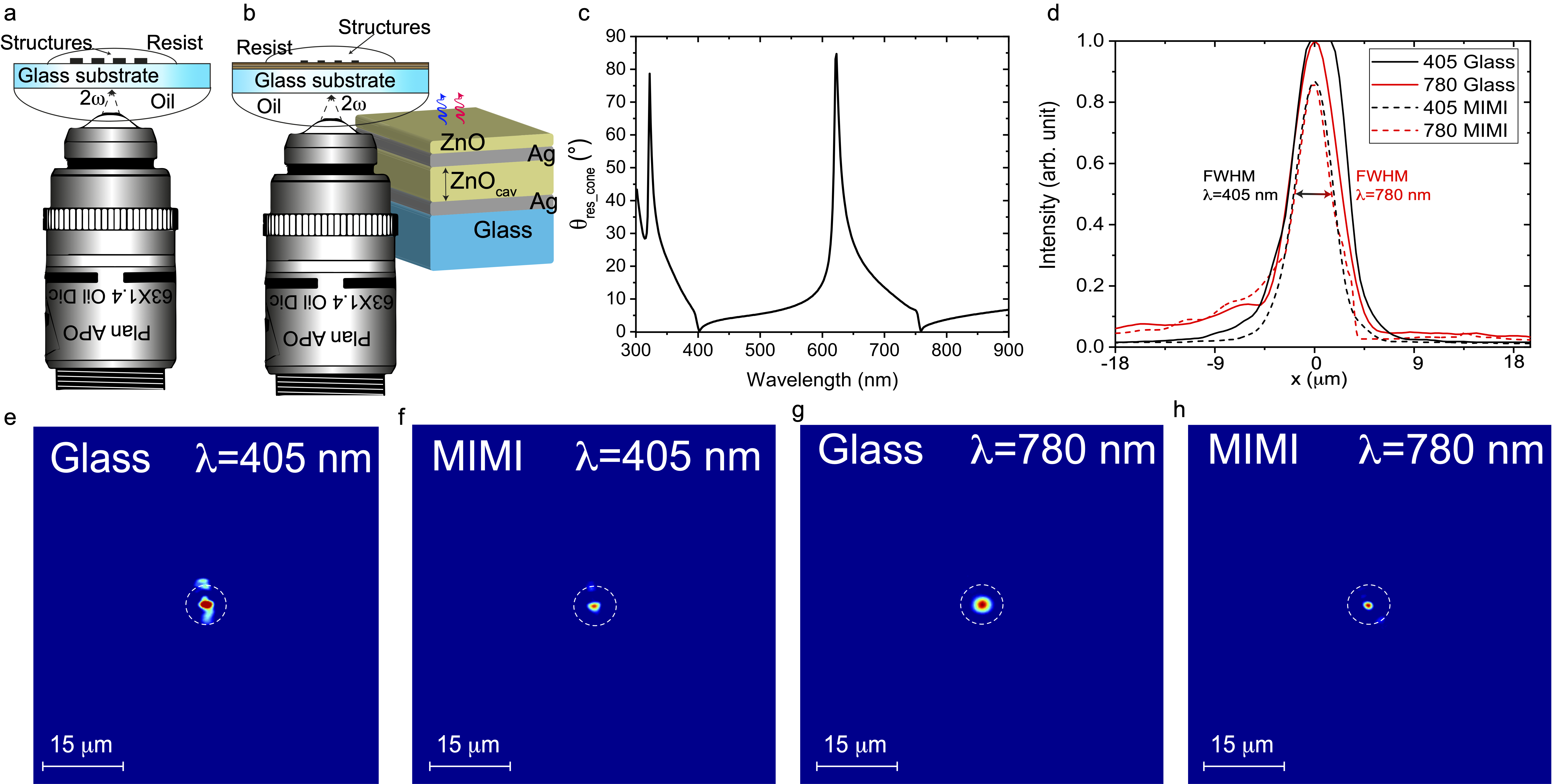
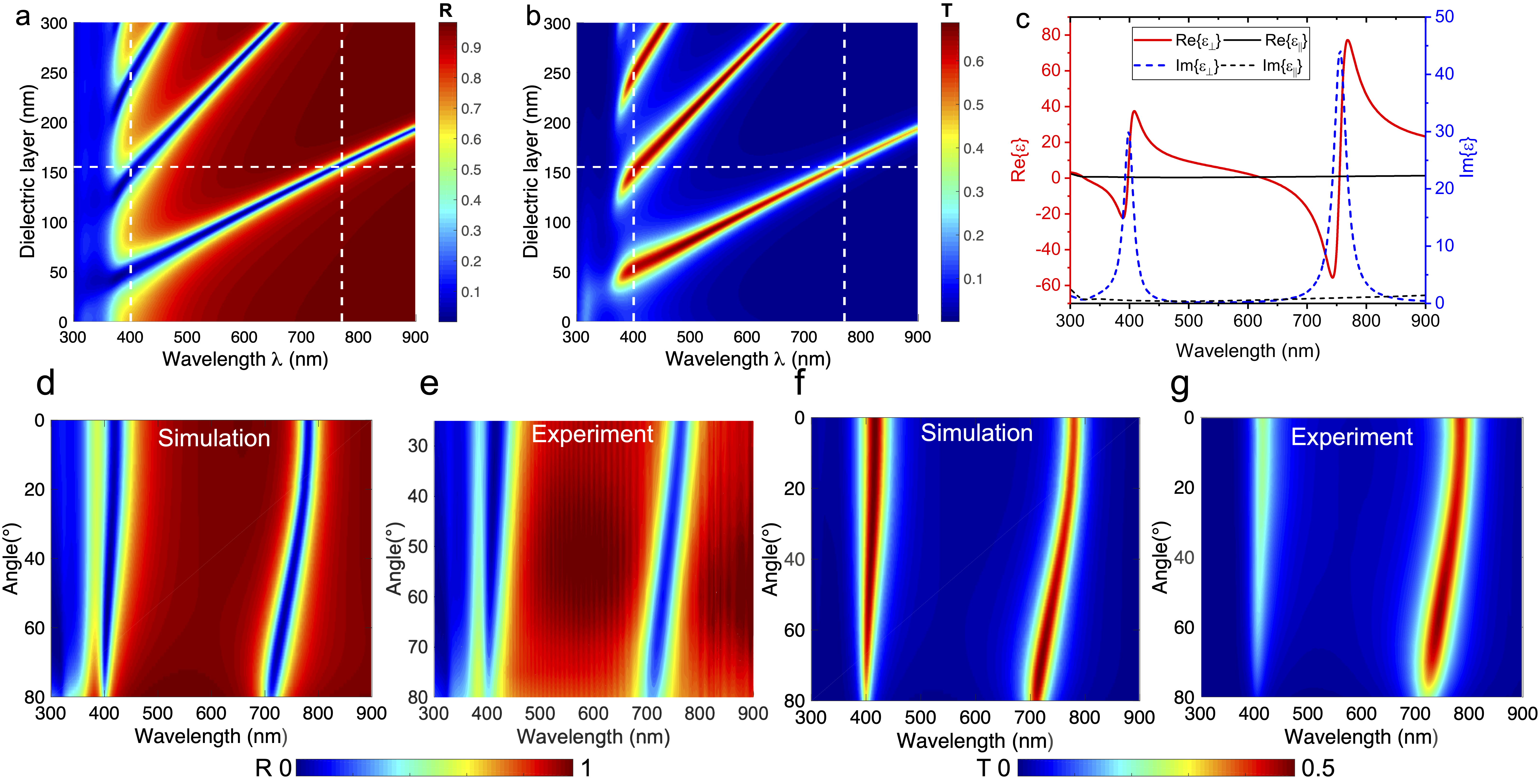
The TP-DLW apparatus used in this work exploits a femtosecond Ti:Sapphire laser () connected to an inverted microscope. The laser beam is focused on the sample through a objective, with 1.4 numerical aperture (NA). 2D and 3D structures can be fabricated through the glass by diving the objective in the photoresist (Fig. 1a). Since the writing process occurs plane by plane, to create the highest reliefs of a structures, the laser beam is attenuated during the travel through the objects already fabricated, generating smaller effective voxels. As illustrated in Fig. 1b, it is possible to drastically increase the resolution in terms of voxel sizes by using a MIMI directly deposited on a classical substrate used for the TP-DLW. The inset reports a schematic view of the MIMI constituted of a silver layer with thickness , a thicker ZnO layer working as an optical nano-cavity (), another silver layer with the same () thickness and a final thin ZnO layer (). In order to obtain a hyper-resolute TP-DLW process, it is necessary that selected wavelengths ( and ) are let through the MIMI device. By using a Finite Element Method (FEM) model, based on numerical ellipsometer analysis (NEA)Lio et al. (2019), and by varying the thickness of the dielectric nano-cavity (), it is possible to retrieve the thickness value to obtain the minimum in reflectance and the maximum in transmittance for a normally incident wave at the two above mentioned wavelengths. In our case, the optimal cavity thickness is that actually supports the plasmonic resonant modes marked with dashed white lines in the reflectance and transmittance maps reported in Figure S1a and b, respectively. A further validation of the occurrence of double modes is provided by a modified effective medium theory (EMT), taking into account the dielectric constant and the thickness of each layer Zeng et al. (1988); Rousselle et al. (1993). This analysis shows the double NZ behavior of the proposed MIMI device presenting the zero crossing point between the real perpendicular and parallel dielectric constant respectively for the two resonant wavelengths (Figure S1c in supplementary material). In case of off-normal light incidence on the same MIMI ( varying from to ) reflectance and transmittance curves are reported in Figures S1d-g. Experimental curves are measured by analyzing the fabricated MIMI by means of a W-VASE ellipsometer, while the numerical analysis is performed again by the NEA model. The quite reliable agreement between numerical and experimental results confirms the possibility to exploit the MIMI for TP-DLW with a focused () laser beam at normal incidence. As reported in past studies Mocella et al. (2009); Pollès et al. (2011); Di Caprio et al. (2012); Arlandis et al. (2012), metamaterials have the remarkable ability to collimate light.
The propagation of light within these metamaterials can be rigorously described by means of the dyadic Green’s function Potemkin et al. (2012). Such an analysis confirms that light emitted in the direction of the extraordinary axis from a localized source placed on the top of metamaterials, propagates within the medium in the so-called resonance cone Newman, Cortes, and Jacob (2013). The resonance cone is visible as two lobes propagating through the medium, separated by a semi-angle , which is calculated as follows Shekhar, Atkinson, and Jacob (2014):
| (1) |
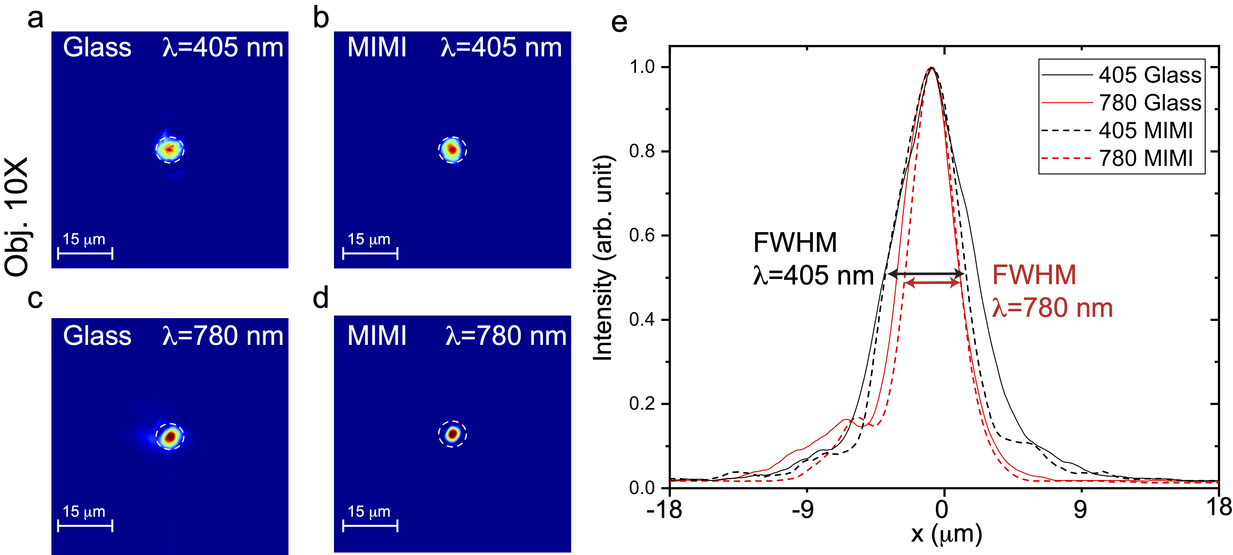
For the considered MIMI device the has been calculated using the parallel and perpendicular dielectric constant retrieved with the EMT. As reported in Figure 1c, the MIMI device presents two points where the resonant cone angle is zero meanimg that, for and , the light passing through the MIMI remains completely collimated. Due to the incident angle independency in the EMT and calculation, the mismatch in terms of desired and evaluated wavelengths is not worrisome. The and the beam behavior is experimentally confirmed by the use of a homebuilt confocal setup (details reported in Figure S2). Each spot has been collected using a beam profiler (Thorlabs BC106N-VIS spectral range from to ). The MIMI is compared with a standard glass (glass coverslip ) used in TP-DLW, the produced focalized spot is measured in order to estimate the beam shrinking by the point spread function (PSF) as illustrated in Figure 1d. The intensity maps are reported in Figures 1e-h. The beam with wavelength of and passing through the MIMI presents a reduction of the initial full width at half maximum (FWHM) of and about , respectively, which corresponds to a reduction of when collected with a 50x objective. In case of a 10x objective, the beam reduction that occurs is about as detailed in the field maps and PSF reported in Figure S3.
III Sample Fabrication and Characterization
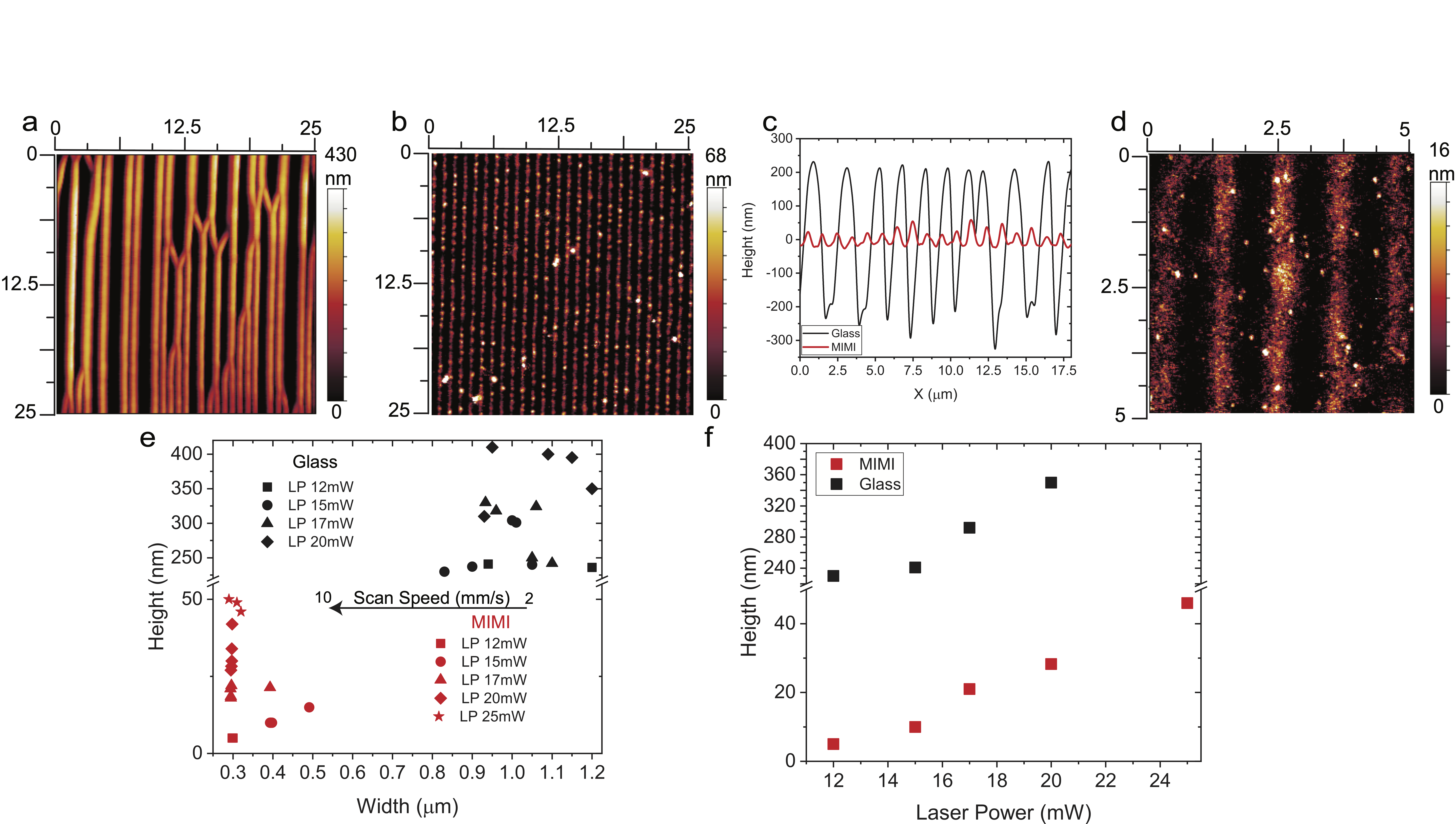
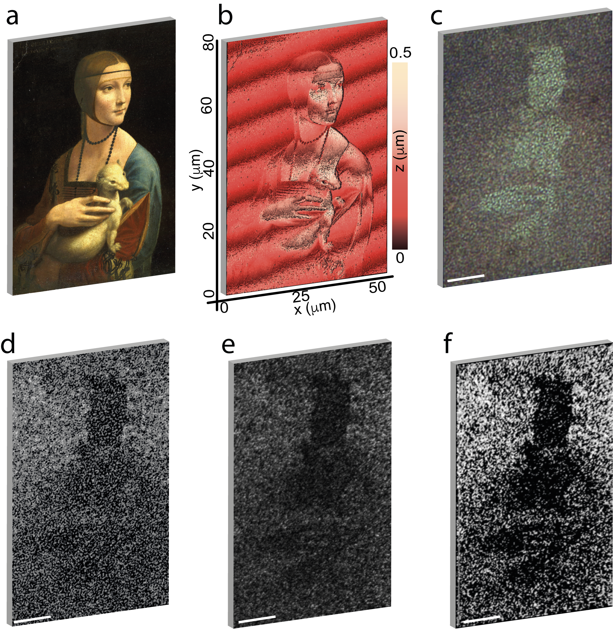
To demonstrate the hyper resolution in a TP-DLW process induced by the presence of a MIMI, an array of 1D gratings has been fabricated on top of the MIMI previously deposited on a glass coversplip substrate. In the latter case, the interface selected to begin the laser writing process is established between the resin and the glass; while in presence of the MIMI, the chosen interface is between the first silver layer and the glass. The use of an array permits to characterize each elements as a function of the laser power , which varies from to , and the scan speed which varies from to . The topography analysis conducted using an atomic force microscope (AFM) with high precision tips (see details in the methods section) ensures to collect very high quality data. A comparison between the AFM measurements performed on the structures realized through a simple glass coverslip and through the MIMI is shown in the Figure 2. The difference between the standard process and through the MIMI stands out immediately offering the possibility to clearly trace straight lines without defects (Figures 2a and b). A comparison between two fabricated gratings, using and , has been done based on the raw images of the AFM profile. As illustrated in Figure 2c, a remarkable difference in terms of height and width of each grating element is present, with a height for the grating made trough glass and an average and and same value for the half width of the MIMI. In Figure 2d, a grating image is reported realized using the lowest laser power and the fastest scan speed producing an and a width . In order to complete and better understand the comparison on both substrates, the size of each grating element contained in the test array have been collected and reported in the graph shown in Figure 2e. The latter evidences an interesting and remarkable difference between the grating sizes produced through the glass and the MIMI. In fact, the resolution is improved in percentage by and in terms of height and width respectively. A further validation has been done by comparing the produced element height at different laser powers. The trend is similar for both substrate maintaining equal the difference that occurs between them as presented in Figure 2f. The proof of concept of the reliability of the proposed technique, able to force the beam self-collimation during writing, is the fabrication of particularly complex three-dimensional TP-DLW tests. The MIMI functionality has been challenged in producing a polymer bas-relief version of the famous Da Vinci’s portrait ”Lady with an Ermine” (Figure 3a). The choice to realize a bas-relief has been done considering that the process involves a 3D lithography and this portrait also contains very tiny details only reproducible in presence of hyper resolution. The first step is create a computer-aided design (CAD) of the portrait image to be used in the TP-DLW process. The obtained design is shown in Figure 3b. The full height of the portrait is chosen as that is divided in slices of thickness each. The optical microscopy image collected by using unpolarized white light and a objective clearly underlines the contours of the portrait and details like face, dress, hand, ermine and necklace (Figure 3c). This high quality optical image is also the consequence of the self-collimation of the microscope impinging light passing through the sample and reaching the objective experimenting the lens effect of the metamaterial as demonstrated in previous worksFang and Zhang (2002); Liu et al. (2007); Casse et al. (2010); Zhao et al. (2011); Kim and Rho (2015). The collection of the whole bas-relief (Figure 3d-e) is obtained by means of a fluorescence confocal microscopy analysis (details in the methods section) performed with a slicing of along the z-axis . This imaging method allows to easily recognize at the minimum height the silhouette of the ”Lady” (Figure 3d). Then by increasing the , the frame shows the details present on top of the sample, as illustrated in Figure 3e. Finally, once the z-stack is completed, by using the proprietary software is possible to recombine all acquired images producing their full overlap and the final picture reported in Figure 3f. The preliminary test highlights the reliability of the hyper resolute 3D TP-DLW with slice distance of and an high level of details reproduced in a very small volume. This technique is foreseen as a valuable possibility to realize anti-counterfeiting tags in the recent research framework of physical unclonable functions.
IV Conclusions
In this work, a novel technique is presented to sensibly improve the performance, in terms of writing resolution, of a generic two-photon direct laser writing process. The diffraction-free ability of an metamaterial enables an extraordinary collimation of the writing laser light and hence the hyper resolution of the TP-DLW. In fabricating test structures like 1D gratings, a reduction of the voxel size of about and , for height and slit width respectively, is observed corresponding for the height of the grating to a reduction from to . The proposed technique gives its best when more complex 3D structures are considered. An hyper-resolute bas-relief version of the famous Da Vinci’s portrait ”Lady with an Ermine” with a full height of only divided in slices of thickness each. These new frontier results find immediate application in the trendsetting scenario of physical unclonable functions and flat-optics.
Methods
Sample fabrication The MIMI substrate is realized by DC sputtering deposition on glass substrate (thickness ), Then, the substrate is placed inside the two-photon lithography apparatus which is able to define the grating pattern or the desired shape in a drop of photo-resine placed on top of the MIMI device. Finally, the sample is developed in a bath of propylene glycol methyl ether acetate (PGMEA) for 25 minutes, then in a bath of isopropanol alcohol (IPA) for other 5 minutes. During all the development process, the sample is soaked.
AFM characterization has been done using a confocal microscope Zeiss LSM 780 equipped with an AFM head-stage. The AFM measurements are performed with high resolute tips with precision of . Each scan has been collected at high resolution of 1024x1024 px in order to reduce any background noise.
Fluorescence Confocal 3D image in fluorescence (see Figures 3) has been acquired using a confocal microscope equipped with a 3D piezoelectric scanner. A 488 nm laser was focused on the cover-slip through a 40x air objective, which allows a spatial resolution of 200 nm, and a z-resolution of 10 nm. The emitted light collected by the objective is sent to a beam-splitter and filtered with a MBS T80/R20. Finally it passes through a pin-hole and is collected by a 580-600 nm detector.
Contributions
G.E.L. conceived the idea. G.E.L., T.R. and A.F. fabricated and fully characterized the structures. G.E.L. and A.F. performed the measurements and analyzed the data. R.C, A.DL. and M.G. devised the experiments and supervised the work. G.E.L. and A.F prepared and wrote the manuscript with input from all authors.
Acknowledgements
The authors thank the Infrastructure “BeyondNano” (PONa3-00362) of CNR-Nanotec for the access to research instruments. They also thank the “Area della Ricerca di Roma 2”, Tor Vergata, for the access to the ICT Services (ARToV-CNR).
References
- Infusino et al. (2012) M. Infusino, A. Ferraro, A. De Luca, R. Caputo, and C. Umeton, “Polycryps visible curing for spatial light modulator based holography,” JOSA B 29, 3170–3176 (2012).
- Sahin, Simsek, and Akturk (2014) R. Sahin, E. Simsek, and S. Akturk, “Nanoscale patterning of graphene through femtosecond laser ablation,” Applied Physics Letters 104, 053118 (2014).
- Sze and Devices (1985) S. Sze and S. Devices, “Physics and technology,” (1985).
- Leclerc, Sakai, and Fujii (2004) E. Leclerc, Y. Sakai, and T. Fujii, “Microfluidic pdms (polydimethylsiloxane) bioreactor for large-scale culture of hepatocytes,” Biotechnology progress 20, 750–755 (2004).
- Psaltis, Quake, and Yang (2006) D. Psaltis, S. R. Quake, and C. Yang, “Developing optofluidic technology through the fusion of microfluidics and optics,” nature 442, 381–386 (2006).
- Ferraro et al. (2018) A. Ferraro, D. C. Zografopoulos, M. A. Verschuuren, D. K. de Boer, F. Kong, H. P. Urbach, R. Beccherelli, and R. Caputo, “Directional emission of fluorescent dye-doped dielectric nanogratings for lighting applications,” ACS applied materials & interfaces 10, 24750–24757 (2018).
- Zhang et al. (2010) Y.-L. Zhang, Q.-D. Chen, H. Xia, and H.-B. Sun, “Designable 3d nanofabrication by femtosecond laser direct writing,” Nano Today 5, 435–448 (2010).
- Li et al. (2009) L. Li, R. R. Gattass, E. Gershgoren, H. Hwang, and J. T. Fourkas, “Achieving /20 resolution by one-color initiation and deactivation of polymerization,” Science 324, 910–913 (2009).
- Bratton et al. (2006) D. Bratton, D. Yang, J. Dai, and C. K. Ober, “Recent progress in high resolution lithography,” Polymers for Advanced Technologies 17, 94–103 (2006).
- Xing et al. (2015) J. Xing, L. Liu, X. Song, Y. Zhao, L. Zhang, X. Dong, F. Jin, M. Zheng, and X. Duan, “3d hydrogels with high resolution fabricated by two-photon polymerization with sensitive water soluble initiators,” Journal of Materials Chemistry B 3, 8486–8491 (2015).
- Lee et al. (2008) K.-S. Lee, R. H. Kim, D.-Y. Yang, and S. H. Park, “Advances in 3d nano/microfabrication using two-photon initiated polymerization,” Progress in Polymer Science 33, 631–681 (2008).
- Tan et al. (2007) D. Tan, Y. Li, F. Qi, H. Yang, Q. Gong, X. Dong, and X. Duan, “Reduction in feature size of two-photon polymerization using scr500,” Applied physics letters 90, 071106 (2007).
- Wu et al. (2010) D. Wu, S.-Z. Wu, L.-G. Niu, Q.-D. Chen, R. Wang, J.-F. Song, H.-H. Fang, and H.-B. Sun, “High numerical aperture microlens arrays of close packing,” Applied physics letters 97, 031109 (2010).
- Passinger et al. (2007) S. Passinger, M. S. Saifullah, C. Reinhardt, K. R. Subramanian, B. N. Chichkov, and M. E. Welland, “Direct 3d patterning of tio2 using femtosecond laser pulses,” Advanced Materials 19, 1218–1221 (2007).
- Park, Yang, and Lee (2009) S.-H. Park, D.-Y. Yang, and K.-S. Lee, “Two-photon stereolithography for realizing ultraprecise three-dimensional nano/microdevices,” Laser & Photonics Reviews 3, 1–11 (2009).
- (16) G. E. Lio, A. Ferraro, M. Giocondo, R. Caputo, and A. De Luca, “Color gamut behavior in epsilon near-zero nanocavities during propagation of gap surface plasmons,” Advanced Optical Materials , 2000487.
- Chen et al. (2013) X. Chen, L. Huang, H. Mühlenbernd, G. Li, B. Bai, Q. Tan, G. Jin, C.-W. Qiu, T. Zentgraf, and S. Zhang, “Reversible three-dimensional focusing of visible light with ultrathin plasmonic flat lens,” Advanced Optical Materials 1, 517–521 (2013).
- Chen et al. (2018) W. T. Chen, A. Y. Zhu, V. Sanjeev, M. Khorasaninejad, Z. Shi, E. Lee, and F. Capasso, “A broadband achromatic metalens for focusing and imaging in the visible,” Nature nanotechnology 13, 220–226 (2018).
- Lio et al. (2019) G. E. Lio, G. Palermo, R. Caputo, and A. De Luca, “A comprehensive optical analysis of nanoscale structures: From thin films to asymmetric nanocavities,” RSC advances 9, 21429–21437 (2019).
- Zeng et al. (1988) X. Zeng, D. Bergman, P. Hui, and D. Stroud, “Effective-medium theory for weakly nonlinear composites,” Physical Review B 38, 10970 (1988).
- Rousselle et al. (1993) D. Rousselle, A. Berthault, O. Acher, J. Bouchaud, and P. Zerah, “Effective medium at finite frequency: Theory and experiment,” Journal of Applied Physics 74, 475–479 (1993).
- Mocella et al. (2009) V. Mocella, S. Cabrini, A. Chang, P. Dardano, L. Moretti, I. Rendina, D. Olynick, B. Harteneck, and S. Dhuey, “Self-collimation of light over millimeter-scale distance in a quasi-zero-average-index metamaterial,” Physical review letters 102, 133902 (2009).
- Pollès et al. (2011) R. Pollès, E. Centeno, J. Arlandis, and A. Moreau, “Self-collimation and focusing effects in zero-average index metamaterials,” Optics express 19, 6149–6154 (2011).
- Di Caprio et al. (2012) G. Di Caprio, P. Dardano, G. Coppola, S. Cabrini, and V. Mocella, “Digital holographic microscopy characterization of superdirective beam by metamaterial,” Optics letters 37, 1142–1144 (2012).
- Arlandis et al. (2012) J. Arlandis, E. Centeno, R. Pollès, and A. Moreau, “From zero-average index metamaterials to zero-dispersion curvature photonic crystal superlattices for self-collimation of light,” in Photonic Crystal Materials and Devices X, Vol. 8425 (International Society for Optics and Photonics, 2012) p. 842510.
- Potemkin et al. (2012) A. S. Potemkin, A. N. Poddubny, P. A. Belov, and Y. S. Kivshar, “Green function for hyperbolic media,” Physical Review A 86, 023848 (2012).
- Newman, Cortes, and Jacob (2013) W. D. Newman, C. L. Cortes, and Z. Jacob, “Enhanced and directional single-photon emission in hyperbolic metamaterials,” JOSA B 30, 766–775 (2013).
- Shekhar, Atkinson, and Jacob (2014) P. Shekhar, J. Atkinson, and Z. Jacob, “Hyperbolic metamaterials: fundamentals and applications,” Nano convergence 1, 14 (2014).
- Fang and Zhang (2002) N. Fang and X. Zhang, “Imaging properties of a metamaterial superlens,” in Proceedings of the 2nd IEEE Conference on Nanotechnology (IEEE, 2002) pp. 225–228.
- Liu et al. (2007) Z. Liu, H. Lee, Y. Xiong, C. Sun, and X. Zhang, “Far-field optical hyperlens magnifying sub-diffraction-limited objects,” science 315, 1686–1686 (2007).
- Casse et al. (2010) B. Casse, W. Lu, Y. Huang, E. Gultepe, L. Menon, and S. Sridhar, “Super-resolution imaging using a three-dimensional metamaterials nanolens,” Applied Physics Letters 96, 023114 (2010).
- Zhao et al. (2011) Y. Zhao, A. A. Nawaz, S.-C. S. Lin, Q. Hao, B. Kiraly, and T. J. Huang, “Nanoscale super-resolution imaging via a metal–dielectric metamaterial lens system,” Journal of Physics D: Applied Physics 44, 415101 (2011).
- Kim and Rho (2015) M. Kim and J. Rho, “Metamaterials and imaging,” Nano Convergence 2, 22 (2015).
Supplementary material
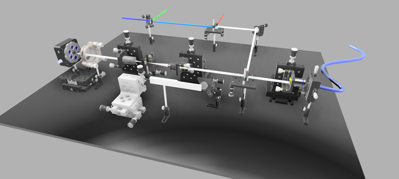
IV.1 Optical Setup
The optical setup for the Point Spread Function (PSF) characterization is composed as following. A collimation line for the white light that is produced by from a Xenon lamp is realized with a 40X objective and a fiber coupler mounted on a 3-axis stage. The collimated in sent to the main confocal line. On the same optical path, it has been placed another 3-axis stage with a 10x objective used only to detect the metalenses on the sample, in fact during the measurements it is moved backward in order to maintain only the collimated light that impinges on the metalens sample. Then, a 32x objective collects the signal from the sample and collimates it into the detector that is represented by a beam profiler (BP) Thorlabs BC106N-VIS spectral range from to mounted on a double-axis stage. A lens collects the signal from the objective and sent it on the BP ccd. In the middle of this path there is the sample mounted on a holder stage that allows controlling micrometer movement. The sample is moved forward and backward along Z in order to collect the beam divergence. Between the fiber collimator and the first objective it has been placed a beam splitter that sends the light from lamp or from the lasers in the main path. The laser line is composed by different lasers. For example a blue laser impinges on a dichroic mirror (DM1) that reflects the green and leads both lasers on a beam splitter (BS1) that collects the red laser and sent all lasers on the second beam splitter (BS2). In order to measure the input power a flip mirror is placed before the 10X objective and the signal is sent on a Thorlabs power meter head (model S130VC). The whole described setup is depicted in Figure S2