Spatially shaping waves to penetrate deep inside a forbidden gap
Abstract
It is well known that waves incident upon a crystal are transported only over a limited distance - the Bragg length - before being reflected by Bragg interference. Here, we demonstrate how to send waves much deeper into crystals, by studying light in exemplary two-dimensional silicon photonic crystals. By spatially shaping the optical wavefronts, we observe that the intensity of laterally scattered light, that probes the internal energy density, is enhanced at a tunable distance away from the front surface. The intensity is up to enhanced compared to random wavefronts, and extends as far as the Bragg length. Our novel steering of waves inside a forbidden gap exploits the transport channels induced by unavoidable deviations from perfect periodicity, here unavoidable fabrication deviations.
Completely controlling wave transport is a key challenge that is essential for a large variety of applications. For instance, classical transport of acoustic waves has enabled sensing, ultrasound imaging and navigation Fink et al. (2000); Cummer et al. (2016). In the quantum regime, control over electron and spin transport has led to major advances in the operation of nanoelectronic devices Neusser and Grundler (2009); Wagner et al. (2016); Klyukin et al. (2018). In photonics, control over light transport has been exploited both in the classical and quantum domain, which has led to rapid advances in science and technology such as solar cells, quantum light sources, optical memories, and micro to nanoscale storage cavities Aspelmeyer et al. (2014); Li and Fan (2018); Tandaechanurat et al. (2011); O’Brien et al. (2009); Kuramochi et al. (2014); Koenderink et al. (2015).
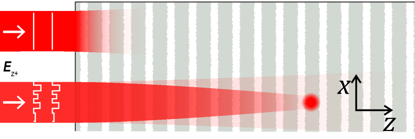
An important tool in wave control is to exploit gap formation as a result of periodic and aperiodic symmetry. The long range periodic order leads to a band structure in the dispersion relations of the waves. Forbidden frequency ranges, stop gaps, emerge in the band structure as a result of interference between the incident waves and Bragg diffracted waves Ashcroft and Mermin (1976); Joannopoulos et al. (2011). Bragg interference causes incident waves with a frequency in the stop gap to be exponentially attenuated, with a characteristic length scale called the Bragg length , as is shown in Fig. 1. The existence of gaps has led to exciting applications such as control of spontaneous emission, efficient light harvesting devices, and biosensing Wehrspohn and Üpping (2012); Inan et al. (2017).
Real crystals feature unavoidable disorder resulting in broken symmetry due to, e.g., thermal motion and phonons in atomic crystals at finite temperature, quantum motion down to zero temperature, or unavoidable structural disorder in assembled photonic or phononic structures Koenderink and Vos (2003). The disorder gives rise to new channels for wave transport due to the multiple scattering, which are typically uncontrolled and thus detrimental for the applications mentioned above. In a specific realization of a crystal the microscopic configuration of disorder is fixed Grishina et al. (2019) and hence the disorder-induced channels do not in themselves offer new control. In disordered media without gaps, however, it is known that spatially shaping the phases of incident waves serves to set interferences between channels that represent new control: wave front shaping Mosk et al. (2012); Vellekoop (2015); Rotter and Gigan (2017).
Therefore, in this paper we set out to demonstrate the tunable control of wave transport in real crystals. By spatially shaping the incident wavefronts as illustrated in Fig. 1, we steer the waves with frequencies within a gap to any desired location. The waves reach a remarkable depth of no less than with more than intensity enhancement. Remarkably, the shaped intensity at in the crystal is even higher than the incident intensity in absence of wave shaping, instead of being Bragg attenuated as is usual in periodic media. In our approach we employ wavefront shaping of light in photonic crystals that can be readily extended to electrons and acoustic waves, where analogous techniques have been demonstrated Harris et al. (2015); Xie et al. (2014).
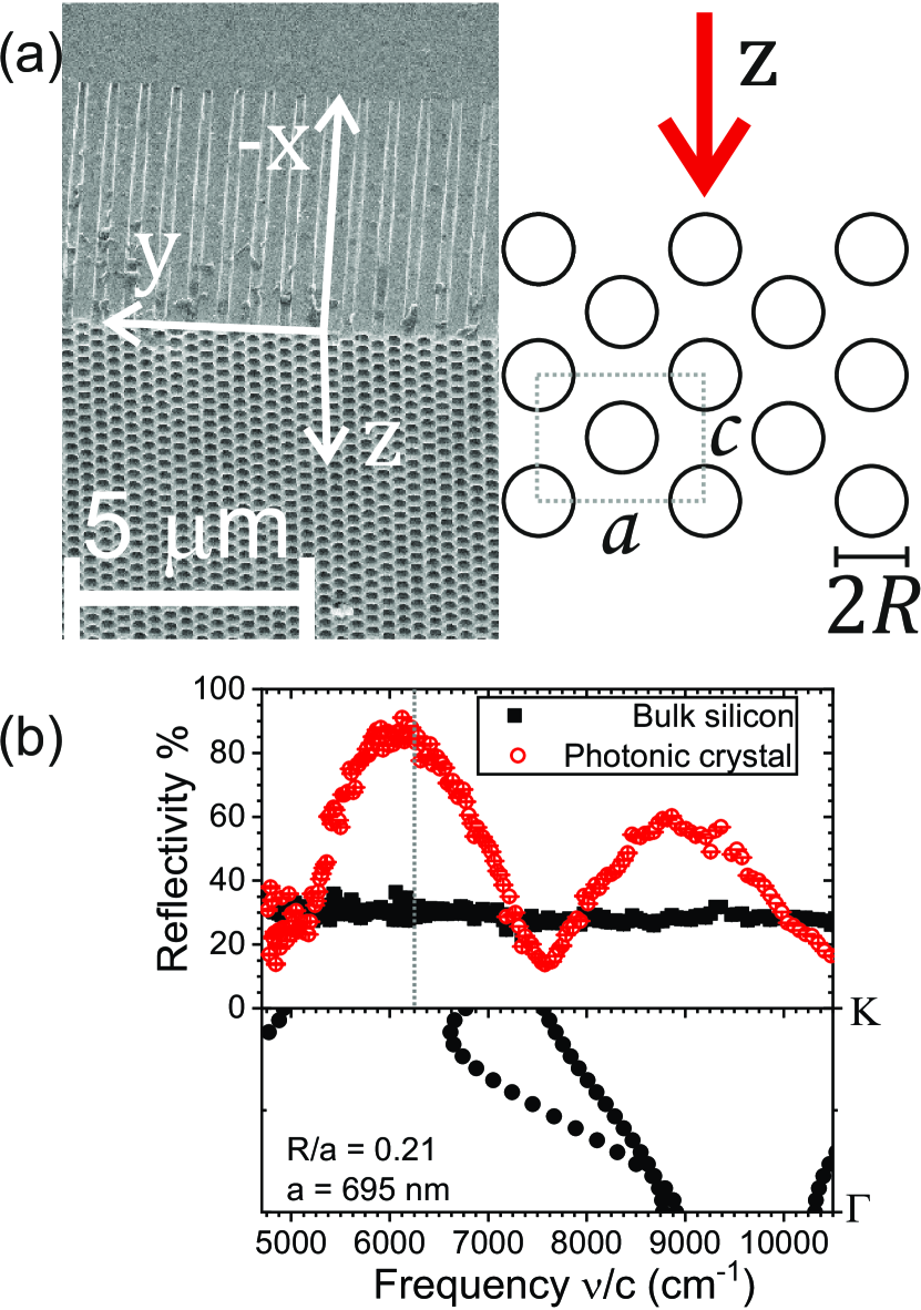
As exemplary waves, we study the propagation of light in two-dimensional (2D) photonic crystals that consist of large periodic arrays of pores etched in a silicon wafer Woldering et al. (2008); Huisman et al. (2012), see Figure 2(a). The pores are made by CMOS-compatible methods, employing deep reactive ion etching though an etch mask. The lateral -extent of the 2D crystal is 10 mm2 at the center of the wafer, much larger than the expected Bragg and scattering length scales. The fabricated pores are about m deep, sufficient for the focus to easily fit within the crystal. The wafers are cleaved in the -plane to expose the 2D photonic crystal to the incident light along the high-symmetry direction Huisman et al. (2012).
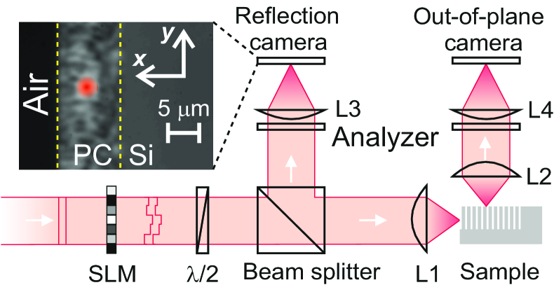
We developed a versatile experimental setup to perform optical wavefront shaping on silicon nanostructures, which operates in the near-infrared spectral range ( nm) where silicon absorption is avoided. The setup consists of three main components: 1) a broadband tunable coherent source, 2) a broadband wavefront shaper, and 3) a twin-arm imaging of reflected and lateral (-plane) scattered signal from the photonic crystal. The broadband tunable coherent source was realized by spectrally filtering the emission from a supercontinuum source using a monochromator. A long pass filter (cut-on wavelength: 850 nm) is used to reject the background from second-order diffraction of shorter wavelengths. The available optical frequencies range from to cm-1, corresponding to wavelengths nm, with a bandwidth of nm and a tuning precision better than nm. The filtered emission is collimated and expanded to a beam diameter of mm.
The wavefront of the collimated beam is then programmed employing a phase-only reflective spatial light modulator SLM (Meadowlark optics; AR coated: 850 – 1650 nm), see Fig. 3. The wavefront-programmed light is imaged to the back focal plane of the large numerical aperture () infrared apochromatic objective lens . The light reflected from the crystal is collected by the same objective. The lateral scattered light from the -plane of the crystal is collected using a long working distance apochromatic objective (). Light collected by either or can be imaged to an InGaAs camera for aligning the incident beam. The inset in Fig. 3 shows the image captured in reflection, where the air, photonic crystal, and the unstructured silicon regions can be clearly separated. The bright spot in the center of the photonic crystal is the focused laser beam when a constant phase () was programmed on the SLM.
Reflectivity from the 2D crystal was measured following the procedures described in Ref. Adhikary et al. (2020). TE-polarized reflectivity spectra shown in Fig. 2(b) reveal two prominent peaks that are identified to correspond to two stops gaps in the calculated band structures. We estimate the Bragg lengths for both gaps from the photonic strength using the relation Vos et al. (2014), where the strength is defined to be Vos et al. (1996). In the two stop bands at cm-1 and cm-1, respectively, the photonic strength is and , respectively, corresponding to Bragg lengths m that are nearly the same for both stop gaps (see Fig. 7 for details).
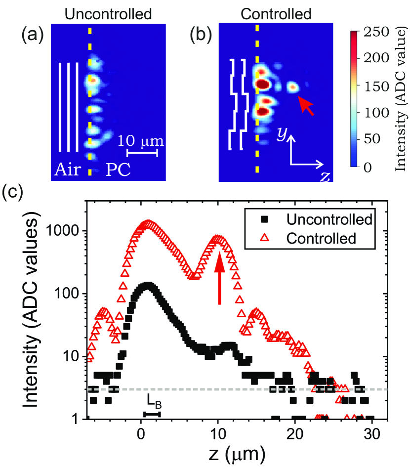
To demonstrate controlled transport of waves, we tune the frequency of the incident light to the center of the first stop gap at cm-1 (i.e. nm). The SLM was initialized with a phase pattern made up of 340 segments (each grouped from 3232 pixels) within the beam diameter, each assigned a random phase in the interval . The size of the segment was chosen to limit the illuminated area on the -plane of the sample to be confined within the photonic crystal. The image of the lateral scattered light collected using is shown in Fig. 4(a), which shows a rapid decay of light into the crystal. The input edge of the crystal is clearly discernible as the bright speckles (also marked by the dashed line).
We target a spot at a depth of m - or - in the crystal and sequentially change the phase of each segment on the SLM to maximize the intensity at the chosen spot. Figure 4(b) shows the image of the lateral scattered light at the end of the iteration over all the segments. A distinct and bright focus is clearly observed at the targeted location, thereby demonstrating the first ever steering of waves inside a crystal, far beyond the Bragg length. Figure 4(c) shows the intensity around the targeted spot before and after steering the light, which shows higher intensity with controlled transport.
In literature, it is common to characterize the quality of wavefront shaping by an enhancement that gauges the intensity increase at the target position Vellekoop and Mosk (2008); Popoff et al. (2014). The enhancement is commonly defined as , where is the optimized intensity in the target spot and is the intensity at the same spot that was ensemble-averaged over 100 random incident wavefront patterns. The intensity of the lateral scattered light is proportional to the energy density of the light that has scattered to a depth in the crystal. The enhancement at the target location inside the crystal is substantial, namely . Remarkably, the intensity at the target spot (depth ) after steering is even greater than the intensity at the front surface () before steering, in contrast to traditional Bragg attenuation of waves inside any periodic medium. The enhancements observed here are a key highlight of the steering of the waves, which takes advantage of the multiple scattering of waves in the crystal due to the deviations from perfect periodicity Koenderink et al. (2005).
Using wavefront shaping, we explore the maximum achievable depth inside the photonic crystal at which the intensity could be enhanced. Figure 5 shows the depth-dependent intensity enhancement at the center of the stop gap (at /c = 6250 cm-1). The error bars represent standard deviations of measured at 8 different spatial locations along at the same depth . An enhancement in excess of 80 was achieved at depths up to m, corresponding to . At a depth of more than , the measured enhancement is . We postulate that the decreasing enhancement with depth arises from the finite thickness of the photonic crystal that is limited by the pore depth. The finite thickness introduces surface losses that prevent the waves from reaching greater depths in the photonic crystal.
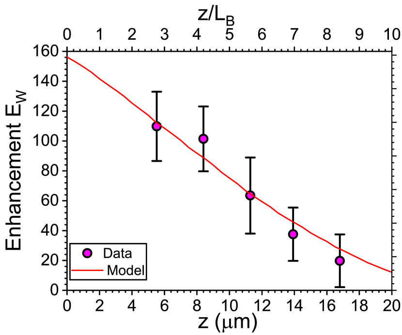
To interpret the intensity enhancement deep inside the crystal, we propose a new model that extends mesoscopic physics typical of random media Evers and Mirlin (2008); Rotter and Gigan (2017) to periodic crystals. The disorder-assisted multiple scattering of light inside the crystal is described using a transmission matrix over the transport channels. The transmission matrix can be decomposed as , where and are unitary matrices of size and is a diagonal matrix with values drawn from the DMPK distribution Dorokhov (1984); Mello et al. (1988); Evers and Mirlin (2008); Akbulut et al. (2016). The wavefront shaping enhancement is proportional to the largest eigenvalue of the matrix , with the proportionality constant set by the wavefront shaping method Vellekoop (2015). The presence of Bragg interference at frequencies within the stop gap and the surface losses result in the attenuation of the multiply scattered waves. This attenuation results in a reduction of the number of transport channels with increasing depth inside the crystal. Mathematically, the reduction in the number of transport channels is modeled as a truncation of the transmission matrix , i.e., a reduced matrix size Goetschy and Stone (2013); Hsu et al. (2015). The reduced number of channels with increasing depth in the crystal is modeled as , where is an amplitude attenuation constant Pendry et al. (1990). The depth-dependent enhancement is the maximum eigenvalue of the truncated transmission matrix. At a given and , we employ a numerical algorithm to generate an ensemble of random transmission matrices and compute the depth-dependent enhancement . The fit to the measured enhancement is shown in Fig. 5 with m-1 and , and is seen to agree very well with the data. To put our model in perspective, the number of control parameters (segments) on the SLM is , which agrees remarkably well with the number of channels in the model. The deviation could arise from the non-uniform intensity incident at each segment of the SLM due to the Gaussian profile of the incident beam. From an independent measurement of the attenuation within the crystal, we extract the intensity extinction length m (see Supplementary Material) arising from the multiple scattering of waves. The intensity attenuation length and the amplitude attenuation constant are related as . From the fit to in Fig. 5, we estimate m, which is smaller than the measured value. The underestimation of is expected as the model effectively accounts for the attenuation due to the Bragg interference and multiple scattering of waves within the crystal, while the measured value is only due to the multiple scattering of waves.
In summary, we have demonstrated controllable enhancement of wave propagation at much greater depths than a Bragg length, even at frequencies within a band gap. We take advantage of transport channels that are introduced in the crystal by unavoidable disorder, and address these by spatially shaping the wavefronts. The large depth to which waves are enhanced, even within a gap, broadens the range of applications feasible with photonic band gap crystals, both 2D and 3D. From the outset, photonic band gaps have been pursued for their radical control over spontaneous emission Lodahl et al. (2004); Fujita et al. (2005), lasing Tandaechanurat et al. (2011), shielding of vacuum noise for qubits Clerk et al. (2010), and for ultimate 3D waveguiding Rinne et al. (2008); Ishizaki et al. (2013). Based on our observations and modeling, light can be reconfigurably steered to resonant and functional features even inside a complete photonic band gap.
Recently, combinations of gaps and tailored disorder are enjoying a fast-growing attention Liew et al. (2011), notably in phononic and photonic quasicrystals Ledermann et al. (2006), and hyperuniform Man et al. (2013); Muller et al. (2017) and bio-mimetic structures Vignolini and Bruns (2018). It is intriguing to speculate whether our crystals may reveal extremal transmission near a Dirac point and pseudo-diffuse behavior as predicted by Sepkhanov et al. on 2D crystals Sepkhanov et al. (2007). Therefore our results open new avenues to increased wave control in many different classes of metamaterials Yves et al. (2017); Ozawa et al. (2019).
Appendix A Spatial resolution of lateral scattered light
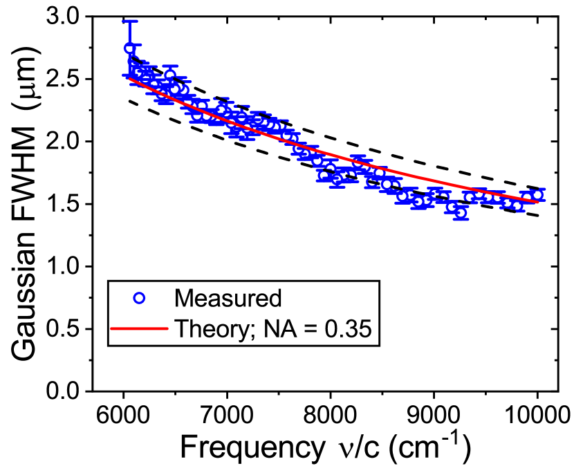
Structural disorder is known to result in a new length scale for wave transport, called extinction length that statistically quantifies the strength of the disorder Akkermans and Montambaux (2007); Wiersma (2013). The extinction length of light in the two-dimensional silicon photonic crystal was characterized by imaging the plane of the sample on a InGaAs camera with an effective optical magnification of 125. A constant phase of 0 rad was displayed on the SLM to focus the light on the sample to a diffraction-limited spot. The images of the lateral scattered light were captured at regular intervals (in nm wavelength steps) as the frequency of the incident light was varied from 6100 cm-1 to 10000 cm-1. The intensity images were integrated along the height, corresponding to the axis. This depth-dependent intensity inside the crystal exhibits an exponential decay convolved with a Gaussian instrument response function, which determines the optical resolution.
Since the precise estimation of the resolution of the lateral scattering imaging setup is important in correctly estimating the extinction length, we first turn to this issue. The peak at the input edge of the photonic crystal was fit with a Gaussian to extract the resolution. Figure 6 shows the Gaussian full-width at half-maximum (FWHM) extracted from the fit. We extract the numerical aperture for the collection arm to be NA = 0.35, which compares well with the nominal collection objective aperture NA = 0.42. It is reasonable that the effective aperture is slightly less than the nominal one, in view of some shadowing by the focusing objective at the input plane (the plane).
Appendix B Extinction length of light in two-dimensional photonic crystals
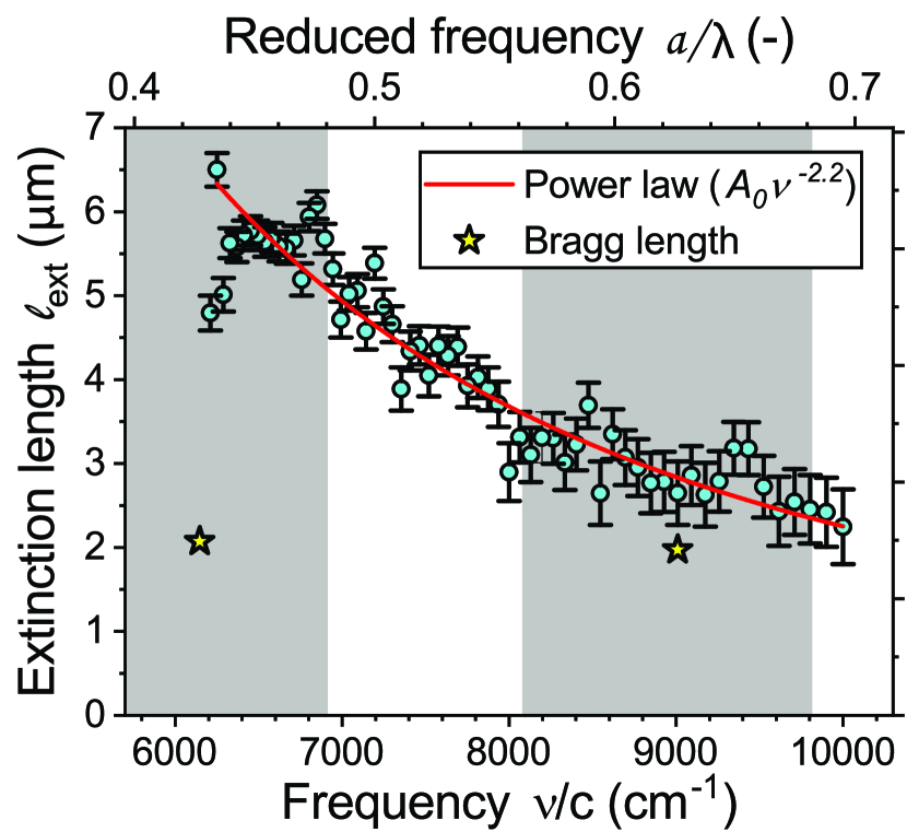
Using the data from Fig. 6, we are now in a position to deconvolve the lateral scattered light with the corresponding Gaussian function. The deconvolved data were matched to a single exponential model to extract the extinction length . Figure 7 shows the extracted (circles) as a function of frequency for TE polarized light incident on the photonic crystal. The error bars correspond to the 95% confidence bound of the fitted extinction length. The extinction length decreases with increasing frequency, as expected, from about m at the lowest frequencies in the first order stop band to about m at the highest frequency beyond the second stop band.
To put these observations in perspective, we compare to theoretical work. Koenderink et al. predicted a power-law dependence of the on the frequency Koenderink et al. (2005). For two-dimensional photonic crystals made of infinite long cylinders, the predicted dependence is , where is a scaling parameter that depends on the degree and nature of the disorder. We adjusted only the scaling parameter to the measured data in Fig. 7 and observe that the power-law dependence on frequency agrees very well with the measurements. The observed deviation at low frequencies in the first stop gap is attributed to our choice of limiting the model to a single exponential to describe the intensity inside the crystal. Inside the stop gap, Bragg interference leads to additional extinction of light with the Bragg length as the characteristic length scale, depicted as star markers in Fig. 7. The two length scales would thus require a bi-exponential model to the intensity attenuation within the crystal, which is at this time difficult to significantly model, given the limited dynamic range and signal to noise ratio of the data. At frequencies in the range of the second stop gap, the Bragg length is close to the extinction length, and thus it is not sensible to try to fit the data with a bi-exponential model.
Appendix C Wave front shaping of light in the photonic crystals
The error bars of the enhancements in Fig. 5 have nearly equal size, independent of the absolute magnitude of the enhancement. We surmise that the enhancement is Gaussian distributed, typical of independent observations, with a standard deviation given by the observed error bar. Conversely, the enhancement does not match with Poisson statistics, where the error bar would grow with magnitude.
Acknowledgements.
We thank Diana Grishina, Ad Lagendijk, Willemijn Luiten, Femi Ojambati, and Allard Mosk (Utrecht) for helpful comments and experimental help. We acknowledge support from NWO-FOM-program“Stirring of light!”, STW-Perspectief program “Free form scattering optics”, and MESA+ Institute section Applied Nanophotonics (ANP).References
- Fink et al. (2000) M. Fink, D. Cassereau, A. Derode, C. Prada, P. Roux, M. Tanter, J.-L. Thomas, and F. Wu, Rep. Progr. Phys. 63, 1933 (2000).
- Cummer et al. (2016) S. A. Cummer, J. Christensen, and A. Alù, Nat. Rev. Mater. 1, 16001 (2016).
- Neusser and Grundler (2009) S. Neusser and D. Grundler, Adv. Mater. 21, 2927 (2009).
- Wagner et al. (2016) K. Wagner, A. Kákay, K. Schultheiss, A. Henschke, T. Sebastian, and H. Schultheiss, Nat. Nanotechnol. 11, 432 (2016).
- Klyukin et al. (2018) K. Klyukin, L. L. Tao, E. Y. Tsymbal, and V. Alexandrov, Phys. Rev. Lett. 121, 056601 (2018).
- Aspelmeyer et al. (2014) M. Aspelmeyer, T. J. Kippenberg, and F. Marquardt, Rev. Mod. Phys. 86, 1391 (2014).
- Li and Fan (2018) W. Li and S. Fan, Opt. Express 26, 15995 (2018).
- Tandaechanurat et al. (2011) A. Tandaechanurat, S. Ishida, D. Guimard, M. Nomura, S. Iwamoto, and Y. Arakawa, Nat. Photonics 5, 91 (2011).
- O’Brien et al. (2009) J. L. O’Brien, A. Furusawa, and J. Vučković, Nat. Photonics 3, 687 (2009).
- Kuramochi et al. (2014) E. Kuramochi, K. Nozaki, A. Shinya, K. Takeda, T. Sato, S. Matsuo, H. Taniyama, H. Sumikura, and M. Notomi, Nat. Photonics 8, 474 (2014).
- Koenderink et al. (2015) A. F. Koenderink, A. Alù, and A. Polman, Science 348, 516 (2015).
- Ashcroft and Mermin (1976) N. W. Ashcroft and N. D. Mermin, Solid state physics (Holt, Rinehart, and Winston, New York, NY, 1976).
- Joannopoulos et al. (2011) J. D. Joannopoulos, S. G. Johnson, J. N. Winn, and R. D. Meade, Photonic crystals: molding the flow of light (Princeton University Press, Princeton, NJ, 2011).
- Wehrspohn and Üpping (2012) R. B. Wehrspohn and J. Üpping, J. Opt. 14, 024003 (2012).
- Inan et al. (2017) H. Inan, M. Poyraz, F. Inci, M. A. Lifson, M. Baday, B. T. Cunningham, and U. Demirci, Chem. Soc. Rev. 46, 366 (2017).
- Koenderink and Vos (2003) A. F. Koenderink and W. L. Vos, Phys. Rev. Lett. 91, 213902 (2003).
- Grishina et al. (2019) D. A. Grishina, C. A. M. Harteveld, A. Pacureanu, D. Devashish, A. Lagendijk, P. Cloetens, and W. L. Vos, ACS Nano 13, 13932 (2019).
- Mosk et al. (2012) A. P. Mosk, A. Lagendijk, G. Lerosey, and M. Fink, Nat. Photonics 6, 283 (2012).
- Vellekoop (2015) I. M. Vellekoop, Opt. Express 23, 12189 (2015).
- Rotter and Gigan (2017) S. Rotter and S. Gigan, Rev. Mod. Phys. 89, 015005 (2017).
- Harris et al. (2015) J. Harris, V. Grillo, E. Mafakheri, G. C. Gazzadi, S. Frabboni, R. W. Boyd, and E. Karimi, Nat. Phys. 11, 629 (2015).
- Xie et al. (2014) Y. Xie, W. Wang, H. Chen, A. Konneker, B.-I. Popa, and S. A. Cummer, Nat. Commun. 5, 1 (2014).
- Woldering et al. (2008) L. A. Woldering, W. R. Tjerkstra, H. V. Jansen, I. D. Setija, and W. L. Vos, Nanotechnology 19, 145304 (2008).
- Huisman et al. (2012) S. R. Huisman, R. V. Nair, A. Hartsuiker, L. A. Woldering, A. P. Mosk, and W. L. Vos, Phys. Rev. Lett. 108, 083901 (2012).
- Adhikary et al. (2020) M. Adhikary, R. Uppu, C. A. Harteveld, D. A. Grishina, and W. L. Vos, Opt. Express 28, 2683 (2020).
- Vos et al. (2014) W. L. Vos, A. Lagendijk, and A. P. Mosk, “Light propagation and emission in complex photonic media,” in Light Localisation and Lasing: Random and Quasi-random Photonic Structures, edited by M. Ghulinyan and L. Pavesi (Cambridge University Press, 2014) p. 1–12.
- Vos et al. (1996) W. L. Vos, R. Sprik, A. van Blaaderen, A. Imhof, A. Lagendijk, and G. H. Wegdam, Phys. Rev. B 53, 16231 (1996).
- Vellekoop and Mosk (2008) I. M. Vellekoop and A. P. Mosk, Phys. Rev. Lett. 101, 120601 (2008).
- Popoff et al. (2014) S. M. Popoff, A. Goetschy, S. F. Liew, A. D. Stone, and H. Cao, Phys. Rev. Lett. 112, 133903 (2014).
- Koenderink et al. (2005) A. F. Koenderink, A. Lagendijk, and W. L. Vos, Phys. Rev. B 72, 153102 (2005).
- Evers and Mirlin (2008) F. Evers and A. D. Mirlin, Rev. Mod. Phys. 80, 1355 (2008).
- Dorokhov (1984) O. N. Dorokhov, Solid State Commun. 51, 381 (1984).
- Mello et al. (1988) P. Mello, P. Pereyra, and N. Kumar, Ann. Phys. 181, 290 (1988).
- Akbulut et al. (2016) D. Akbulut, T. Strudley, J. Bertolotti, E. P. A. M. Bakkers, A. Lagendijk, O. L. Muskens, W. L. Vos, and A. P. Mosk, Phys. Rev. A 94, 043817 (2016).
- Goetschy and Stone (2013) A. Goetschy and A. Stone, Phys. Rev. Lett. 111, 063901 (2013).
- Hsu et al. (2015) C. W. Hsu, A. Goetschy, Y. Bromberg, A. D. Stone, and H. Cao, Phys. Rev. Lett. 115, 223901 (2015).
- Pendry et al. (1990) J. Pendry, A. MacKinnon, and A. Pretre, Physica A 168, 400 (1990).
- Lodahl et al. (2004) P. Lodahl, A. F. Van Driel, I. S. Nikolaev, A. Irman, K. Overgaag, D. Vanmaekelbergh, and W. L. Vos, Nature (London) 430, 654 (2004).
- Fujita et al. (2005) M. Fujita, S. Takahashi, Y. Tanaka, T. Asano, and S. Noda, Science 308, 1296 (2005).
- Clerk et al. (2010) A. A. Clerk, M. H. Devoret, S. M. Girvin, F. Marquardt, and R. J. Schoelkopf, Rev. Mod. Phys. 82, 1155 (2010).
- Rinne et al. (2008) S. A. Rinne, F. García-Santamaría, and P. V. Braun, Nat. Photonics 2, 52 (2008).
- Ishizaki et al. (2013) K. Ishizaki, M. Koumura, K. Suzuki, K. Gondaira, and S. Noda, Nat. Photonics 7, 133 (2013).
- Liew et al. (2011) S. F. Liew, J.-K. Yang, H. Noh, C. F. Schreck, E. R. Dufresne, C. S. O’Hern, and H. Cao, Phys. Rev. A 84, 063818 (2011).
- Ledermann et al. (2006) A. Ledermann, L. Cademartiri, M. Hermatschweiler, C. Toninelli, G. A. Ozin, D. S. Wiersma, M. Wegener, and G. Von Freymann, Nat. Mater. 5, 942 (2006).
- Man et al. (2013) W. Man, M. Florescu, E. P. Williamson, Y. He, S. R. Hashemizad, B. Y. Leung, D. R. Liner, S. Torquato, P. M. Chaikin, and P. J. Steinhardt, Proc. Natl. Acad. Sci. U.S.A. 110, 15886 (2013).
- Muller et al. (2017) N. Muller, J. Haberko, C. Marichy, and F. Scheffold, Optica 4, 361 (2017).
- Vignolini and Bruns (2018) S. Vignolini and N. Bruns, Adv. Mater. 30, 1801687 (2018).
- Sepkhanov et al. (2007) R. A. Sepkhanov, Y. B. Bazaliy, and C. W. J. Beenakker, Phys. Rev. A 75, 063813 (2007).
- Yves et al. (2017) S. Yves, R. Fleury, T. Berthelot, M. Fink, F. Lemoult, and G. Lerosey, Nat. Commun. 8, 16023 (2017).
- Ozawa et al. (2019) T. Ozawa, H. M. Price, A. Amo, N. Goldman, M. Hafezi, L. Lu, M. C. Rechtsman, D. Schuster, J. Simon, O. Zilberberg, and I. Carusotto, Rev. Mod. Phys. 91, 015006 (2019).
- Akkermans and Montambaux (2007) E. Akkermans and G. Montambaux, Mesoscopic physics of electrons and photons (Cambridge University Press, Cambridge, UK, 2007).
- Wiersma (2013) D. Wiersma, Nat. Photonics 7, 188 (2013).