Tuning Magnetic Properties of Penta-Graphene Bilayers Through Doping with Boron and Oxygen
Abstract
Penta-graphene (PG) is a carbon allotrope that has recently attracted the attention of the materials science community due to its interesting properties for renewable energy applications. Although unstable in its pure form, it has been shown that functionalization may stabilize its structure. A question that arises is whether its outstanding electronic properties could also be further improved using such a procedure. As PG bilayers present both sp2 and sp3 carbon planes, it consists of a flexible candidate for functionalization tuning of electromagnetic properties. In this work, we perform density functional theory simulations to investigate how the electronic and structural properties of PG bilayers can be tuned as a result of substitution doping. Specifically, we observed the emergence of different magnetic properties when boron was used as dopant species. On the other hand, in the case of doping with oxygen, the rupture of bonds in the sp2 planes does not induce a magnetic moment in the material.
Introduction
The interest in two-dimensional extended nanostructures was further highlighted after graphene was obtained by the Novoselov group [1, 2]. The properties of graphene are truly unique [3], and a wide range of applications have been predicted for this carbon allotrope [4]. Although the overall success of graphene, there are still some limitations to be overcome regarding its optoelectronic applications, the main being its null bandgap [5]. For that reason, other two-dimensional materials have been extensively tested. Among them, the transition metal dichalcogenides (TMDs) [6, 7, 8] and novel graphene-based allotropes [9, 10, 11] stand out. However, graphene allotropes still hold the important advantage over TMDs, for instance, of being formed only by carbon atoms, which makes it easier to synthesize on a large scale. Therefore, it would be ideal to conceive a material that, while presenting semiconducting properties would still be based on graphene.
Having such a goal in mind, several theoretical and experimental studies have been conducted to achieve alternative solutions to monolayer graphene [9, 10, 12, 13, 11, 14, 15, 16, 17]. For instance, studies concerning graphene bilayer have concluded that its structural properties can be altered from a suitable layer stacking engineering [18, 19, 20]. In one of these studies, it was obtained that the rotation of one graphene layer over another leads to the displacement of the Dirac cones, but no gap opening was observed [18]. The conclusion is that layer stacking still need to be associated with other procedure if a graphene-based system with semiconducting properties is to arise. So far, the main option relied on substitutional doping [21, 22, 23, 24] on graphene structure. Density functional theory calculations were performed to study the doping of boron (B) and nitrogen (N) in graphene bilayers [25]. The results revealed that for doping with B (N), a gap opening from 0.11 to 0.32 eV (0.09 and 0.30 eV) was obtained, being these values depend on the type of bilayers packing [25].
Another approach is to study other possible arrangements: different, and yet based on graphene. Among them are carbon nanotubes [26], nanoribbons [27], nanoscrolls [28], and novel graphene-based allotropes, such as popgraphene [11], phagraphene [10], and penta-graphene [9] (PG). In its pure form, the PG structure is meta-stable but presents an almost direct bandgap eV, which is interesting for optoelectronic applications. Its structure is similar to the pentagonal tiles of Cairo, where the carbon atoms occupy three types of planes: a plane of sp3 carbons sandwiched by two planes of sp2 carbons [9]. Such a structure allows more degrees of freedom for doping when contrasted to graphene. As a result, different ways of modulating its electronic properties can be obtained [29]. Particularly, it can be reasoned that the flexibility of such material makes it a promising candidate to fulfill the role of the carbon allotrope with semiconducting-like properties. This fact is especially true if one considers the two promising factors on PG: considering bilayers and substitutional doping.
It is well known that the PG bandgap increases with an increase in oxygen doping concentration [30, 31, 32]. Such a trend is attributed to the up-shift of the conduction band minimum during the oxidation process [30]. Since oxidized PG exhibits a large bandgap, it can be considered as a good alternative for the conception of new dielectric layers in electronic devices [31]. When it comes to doped carbon-based nanostructures, boron is the most often used dopant once its similar electronic structure and size to carbon allow its incorporation into the carbon-based substrate with minimal strain and changes in the lattice arrangement [33, 34, 35, 36, 37, 38]. Moreover, the boron-doped PG can effectively decompose H2 molecules into two H atoms, which is an interesting feature for energy conversion and storage applications [36]. In this sense, oxygen- and boron-doped PG systems must be further studied to propose new routes in developing PG-based devices.
Herein, motivated by the fact that PG has more degrees of freedom to modulate its electronic properties than graphene, we have explored its electronic properties in doped bilayers by carrying out state of art electronic structure calculations on the Density Functional Theory (DFT) level of theory. We studied the effects of boron and oxygen as substitutional dopants in the different hybridization planes of the PG structure. It was observed that the introduction of oxygen atoms in the sp2 plane leads to the breaking of bonds and subsequently no magnetic properties take place. Remarkably, boron doping in the sp3 plane, in turn, gives rise to a significant magnetization which was not observed for the cases in which this dopant was introduced in the sp2 plane. As mentioned above, PG packing allows us to have extra degrees of freedom for doping. This feature is interesting since in PG monolayers there are two sp2 planes that can interact with the external environment. This, in turn, creates another degree of freedom for doping and, consequently, for modulation of its electronic properties.
Results
We begin our discussions by presenting the structural properties and the charge localization profiles for the model doped PG bilayers studied here. In this sense, Figure 1 shows the schematic representation of optimized PG bilayers doped with boron and oxygen (top panels), the bond lengths on the neighboring of the doping sites (middle panels), and charge density distribution of the system (bottom panels). Figure 1(a) presents the optimized geometry of the two layers without defects, i.e. before the doping procedure took place. Figures 1(b-d) represent the substitutional doping with boron, whereas Figures 1(e-g) account for the oxygen-based functionalization. In the doping mechanism adopted here, the PG plane at the bottom is always pristine. The second PG layer on top receives the dopant in three distinct channels: (dopant-sp2-out) when the dopant is placed in the plane above the interlayer region interacting with the vacuum, (dopant-sp2-in) when the dopant is placed in the plane within the interlayer region interacting with the PG plane at the bottom, and (dopant-sp3) for the doping in the sp3 plane. For these nomenclatures, “dopant” stands for oxygen (O) or boron (B) atom. Importantly, some theoretical works have studied the structural stability of oxygen- and boron-doped PG layers [36, 39]. In a reactive molecular dynamics study, the results have revealed that oxygen-doped PG layers present remarkable enhancement in failure stress and strain when contrasted with pristine PG layers [39]. Moreover, it was recently demonstrated, by using DFT calculations, that boron-doped PG layers are structurally stable when concentrated with pristine PG layers [36].
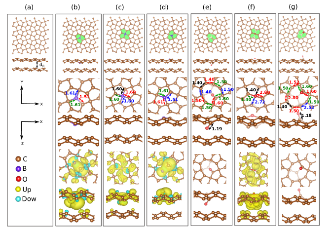
Figures 1(b), 1(c), and 1(d) illustrate the cases B-sp2-in, B-sp3, and B-sp2-out, respectively. One can observe that the bond lengths between slightly deviate from that of the bond length in the pristine monolayer, which is 1.57 Å. These bond lengths () assume minimum and maximum values of 1.51 to 1.61 Åfor all the cases of doping with B. As for the oxygen doping picture, represented by Figures 1(e-g), we observe a greater deformation around the doping site. Figures 1(e) and 1(g) show the result of doping the sp2 planes. It is possible to note a tendency of carbonyl formation with the elevation of the oxygen atom by the distance of 1.18 and 1.19 Åfrom the carbon atom in the respective sp3 plan. With the elevation of the oxygen from the sp2 plane, the formation of a vacancy is observed with bond lengths in the edges whose sizes vary from 1.40 to 1.60 Åfor the case O-sp2-in and O-sp2-out. In the case O-sp3 (Figure 1(f)), a tendency of the oxygen to leave the plane is also observed, as the bond length of 1.40 to 1.72 Åis achieved between the first neighbors of the dopant.
The bottom panels of Figure 1 provide a representation of the charge density wrapped around the dopant. The yellowish cloud stands for the density due to up spin electrons, whereas the blueish on of the down spin electrons. The net charge observed is responsible for the magnetic moment, which characterizes a magnetization due to the presence of the dopant. The values of the magnetic moment for each structure are listed in Table 1, to be discussed later. It is observed that this charge concentration is more effective in the case of doping with boron. On the other hand, no spontaneous magnetization was observed in the O-sp2-in and O-sp2-out cases. This behavior suggests that magnetization in the case of doping with oxygen is not a direct consequence of doping, but rather of the deformation of the geometry that the dopant produces. The sp3 plane has two dangling carbons with a distance of 2.80 and 2.72 Åfrom the oxygen atom. This distance makes the -electrons of these two atoms to contribute to the effective magnetization of the bilayer, whose magnetic moment is 2.00 Bohr Magneton. In the O-sp2-in and O-sp2-out cases, the non-concentration of charge in the oxygen atom, which makes two connections in the plane, suggests a double bonding with the carbon, which characterizes a carboxyl. The resulting bond configuration for the carbon atoms in the edge keeps the symmetry of the vacancy.
| B-sp2-in | B-sp3 | B-sp2-out | O-sp2-in | O-sp3 | O-sp2-out | |
|---|---|---|---|---|---|---|
| Eform (eV) | -9.54 | -9.55 | -9.39 | 9.60 | -9.59 | -9.41 |
| Ecoh (eV) | -8.38 | -8.37 | -8.37 | -8.42 | -8.48 | -8.42 |
| m () | 1.00 | 0.93 | 1.00 | 0.00 | 2.00 | 0.00 |
| d0 (Å) | 3.12 | 2.50 | 2.60 | 2.70 | 2.60 | 2.60 |
The first row of Table 1 presents the formation energy, which is defined as: , where is the total energy for each doped bilayer, the total energy of the monolayer without defect, and Emd total energy of the doped bilayer. One can observe that the energy cost for the formation of the bilayer is approximately the same for the two types of doping, i.e., -9.39 to -9.60 eV for boron and oxygen, respectively. In the second row of this table, we present the cohesion energy that is given by , where is the total energy of a carbon atom and is the number of carbon atoms of the bilayer. and are the total energies and number of doping atoms respectively, where stands for B or O. is the total number of atoms in the bilayers. The cohesion energy has values similar for all systems, suggesting the same level of cohesion for the two types of dopants. In the third row, we present the magnetic moment of each bilayer. One can realize that for the O-sp3 case, the value of the magnetic moment is zero, which is in agreement with what was already discussed of the net charge density. In the fourth row, the distances between the two layers are shown. After optimizing the geometry of the bilayers, these distances remained larger for the two both B-sp2-in and O-sp2-in doping cases, compared to the others that were between 2.50 and 2.60 Å, while for B-sp2-in and O-sp2-in is 3.12 and 2.70 Å, respectively. These results suggest that the dopant has a significant contribution to the interactions between the two layers.
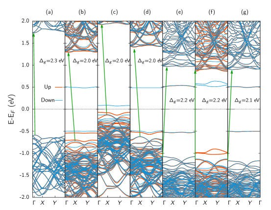
Figure 2 presents the band structure of the doped bilayer bands. For the pure bilayer (Figure 2(a)), one can note that an almost indirect gap of 2.3 eV takes place, a value approximately equal to that found for the PG monolayer [9]. In the case of doping with boron, we observe a reduction of the bandgap to 2.0 eV, which remained indirect. For the two cases of sp2 doping (Figures 2(b) and 2(d)), it occurs the emergence of states in the middle of the bandgap: a downstate above the Fermi level, one up and other down states, below the Fermi level. These states characterize the magnetization of the system. For the sp3 (Figure 2(c)), the two states in the middle of the bandgap are symmetrical, with spin up and down above and below the Fermi level, respectively. In the case of oxygen doping, we also observed the appearance of the states in the middle of the Fermi level: these states are symmetrical concerning the Fermi level and have no spin degeneration for the O-sp2-in and O-sp2-out cases (Figures 2(e) and 2(g)). In these configurations, the bandgap was reduced to 2.2 and 2.1 eV, respectively. For the O-sp3 case (Figure 2(f)), the bandgap is also 2.2 eV and with the two symmetrical states about the Fermi level, with spin up below and down above the Fermi Level.
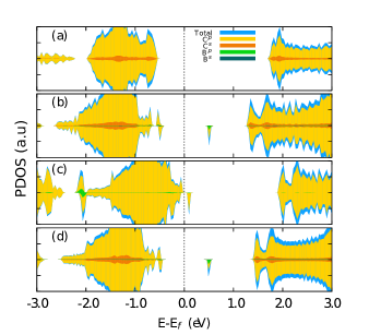
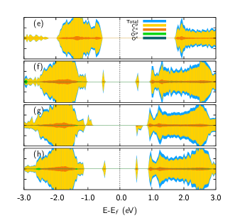
Finally, Figure 3 presents the projected density of states (PDOS). In the cases of boron doping, one can realize that for the pristine bilayer (Figure 3(a)) the most significant contribution to the formation of the bands is for the states of carbon atoms. The Fermi level is closer to the valence bands, which characterizes a -type semiconductor. As for the B-sp3 cases (Figures 3(b) and 3(d)), a slight contribution of orbitals of boron at the first peak in the middle of the bandgap (above the Fermi level) is observed. Still, for these two cases, we observed that the Fermi level is closer to the valence band, which characterizes a -type semiconductor. Regarding the B-sp3 case (Figure 3(c)), there is no significant contribution of boron to the states near the Fermi level and the structure behaves as a -type semiconductor, once the Fermi level is touching the top of the valence band. In the case of oxygen doping (Figures 3(e-h)), we did not observe any significant contribution from O atoms. In the O-sp2-in case (Figure 3(f)), the Fermi level is in the middle of the bandgap with peaks symmetrically localized regarding it for both spin channels, which characterizes the non-magnetization of this material. In the O-sp3 case (Figure 3(g)), we have observed that the Fermi level is slightly displaced towards the conduction states, which characterizes a -type semiconductor. It is also observed antisymmetric peaks in relation to the spin, which stands for a significant magnetic moment of this structure. For the O-sp2-out case (Figure 3(h)), a slight displacement of the Fermi level near the conduction band was also observed, characterizing a -type semiconductor. It is observed that the peaks closest to the Fermi level are symmetrical in relation to the spin states, proving the non-magnetic behavior of the material.
Methods
To investigate the electronic structure of doped PG bilayers, we used DFT calculations as implemented in the SIESTA software [40, 41]. It makes use of a numerical base to expand the wave functions of the many atoms system. In the present work, it was used the DZP basis set [42, 43]. As for the functional approximation, it was considered the generalized approximation of the gradient proposed by Perdew, Burke and Ernzerhof (GGA/PBE) + vDW [44], which is built from the expansion of the second-order density gradient. Pseudopotentials parameterized within the Troullier-Martins formalism are also considered [45]. This approximation is of fundamental importance for the description of the magnetic and electronic properties of materials composed of atoms with many electrons. All calculations were performed considering spin polarization. To calculate the bands and state densities, an MPK mesh of 15 x 15 x 1 is used [46]. A mesh cut of 200 Ry is chosen as a parameter for our calculations [47]. The forces converged until reaching a minimum value of 0.001 eV/Å. In order to ensure a good compromise between the accuracy of our results and the computational feasibility, the tolerance in the density of the matrix and in the total energy was set at 0.0001 and 0.00001 eV, respectively. Importantly, this set of parameters were used recently to study other carbon-based lattices [29, 48, 49, 50].
Conclusion
In summary, we carried out DFT calculations to investigate the influence of boron and oxygen doping on the electronic properties of PG bilayers. Our findings showed that the difference between dopant on the sp2 and sp3 planes have a significant impact on the magnetic properties of oxygen doping. As for the case of doping with boron, it was observed a spontaneous magnetization in the system. This is due to the fact that boron contains only one electron in the orbital valence , whereas the substituted carbon has a pair of electrons in this same orbital. Therefore, the bond results in a magnetic polarization due to electronic covalence, leading to the emergence of two electrons with the same spin and one electron with the opposite spin. This effect is characterized by three flat energy levels that appear in the middle of the bandgap for the case of boron doping in the sp2 planes. Such an effect is not observed in the case of doping with oxygen due to bond breaking. Regarding the effect on the pristine layer, there was no significant difference in its electronic properties. In the cases of boron doping, the resulting system characterizes a -type semiconductor. On the other hand, for the oxygen doping in the sp3 plane, we have observed that the Fermi level is slightly displaced towards the conduction states, which characterizes a 0-type semiconductor. Since the electronic structure of PG bilayers present extra doping channels and can be easily tuned by doping its structure with just a single atom, they can represent an interesting alternative for replacing graphene in some optoelectronic applications.
References
- [1] Novoselov, K. S. et al. Electric field effect in atomically thin carbon films. \JournalTitleScience 306, 666–669, DOI: 10.1126/science.1102896 (2004).
- [2] Geim, A. & Novoselov, K. The rise of graphene. \JournalTitleNature Mater 6, 183–191, DOI: https://doi.org/10.1038/nmat1849 (2007).
- [3] Lin, Y.-M. et al. Wafer-scale graphene integrated circuit. \JournalTitleScience 332, 1294–1297, DOI: 10.1126/science.1204428 (2011).
- [4] Liu, M. et al. A graphene-based broadband optical modulator. \JournalTitleNature 474, 64–67, DOI: https://doi.org/10.1038/nature10067 (2011).
- [5] Novoselov, K. Mind the gap. \JournalTitleNature Mater 6, 720–721, DOI: https://doi.org/10.1038/nmat2006 (2007).
- [6] Qiu, H. et al. Hopping transport through defect-induced localized states in molybdenum disulphide. \JournalTitleNature communications 4, 2642 (2013).
- [7] Luo, X. et al. Effects of lower symmetry and dimensionality on raman spectra in two-dimensional wse2. \JournalTitlePhys. Rev. B 88, 195313, DOI: 10.1103/PhysRevB.88.195313 (2013).
- [8] Jones, A. et al. Optical generation of excitonic valley coherence in monolayer wse2. \JournalTitleNature Nanotechnology 8, 634–638, DOI: 10.1038/nnano.2013.151 (2013).
- [9] Zhang, S. et al. Penta-graphene: A new carbon allotrope. \JournalTitleProceedings of the National Academy of Sciences 112, 2372–2377 (2015).
- [10] Wang, Z. et al. Phagraphene: a low-energy graphene allotrope composed of 5–6–7 carbon rings with distorted dirac cones. \JournalTitleNano letters 15, 6182–6186 (2015).
- [11] Wang, S., Yang, B., Chen, H. & Ruckenstein, E. Popgraphene: a new 2d planar carbon allotrope composed of 5–8–5 carbon rings for high-performance lithium-ion battery anodes from bottom-up programming. \JournalTitleJournal of Materials Chemistry A 6, 6815–6821 (2018).
- [12] Li, X., Wang, Q. & Jena, P. -graphene: a new metallic allotrope of planar carbon with potential applications as anode materials for lithium-ion batteries. \JournalTitleThe journal of physical chemistry letters 8, 3234–3241 (2017).
- [13] Jiang, J.-W. et al. Twin graphene: A novel two-dimensional semiconducting carbon allotrope. \JournalTitleCarbon 118, 370–375 (2017).
- [14] Meng, F., Ni, M., Chen, F., Song, J. & Wei, D. Nanoscale fracture of defective popgraphene monolayers. \JournalTitlePhys. Chem. Chem. Phys. 21, 1242–1253, DOI: 10.1039/C8CP06577B (2019).
- [15] Toh, C.-T. et al. Synthesis and properties of free-standing monolayer amorphous carbon. \JournalTitleNature 577, 199–203, DOI: 10.1038/s41586-019-1871-2 (2020).
- [16] Joo, W.-J. et al. Realization of continuous zachariasen carbon monolayer. \JournalTitleScience Advances 3, DOI: 10.1126/sciadv.1601821 (2017).
- [17] Falcao, E. H. & Wudl, F. Carbon allotropes: beyond graphite and diamond. \JournalTitleJournal of Chemical Technology & Biotechnology 82, 524–531, DOI: 10.1002/jctb.1693 (2007).
- [18] Lopes dos Santos, J. M. B., Peres, N. M. R. & Castro Neto, A. H. Graphene bilayer with a twist: Electronic structure. \JournalTitlePhys. Rev. Lett. 99, 256802, DOI: 10.1103/PhysRevLett.99.256802 (2007).
- [19] Qiao, J.-B., Yin, L.-J. & He, L. Twisted graphene bilayer around the first magic angle engineered by heterostrain. \JournalTitlePhys. Rev. B 98, 235402, DOI: 10.1103/PhysRevB.98.235402 (2018).
- [20] Bistritzer, R. & MacDonald, A. H. Moiré bands in twisted double-layer graphene. \JournalTitleProceedings of the National Academy of Sciences 108, 12233–12237, DOI: 10.1073/pnas.1108174108 (2011).
- [21] Coletti, C. et al. Charge neutrality and band-gap tuning of epitaxial graphene on sic by molecular doping. \JournalTitlePhys. Rev. B 81, 235401, DOI: 10.1103/PhysRevB.81.235401 (2010).
- [22] Zhou, S. Y., Siegel, D. A., Fedorov, A. V. & Lanzara, A. Metal to insulator transition in epitaxial graphene induced by molecular doping. \JournalTitlePhys. Rev. Lett. 101, 086402, DOI: 10.1103/PhysRevLett.101.086402 (2008).
- [23] Zhou, S. Y. et al. Substrate-induced bandgap opening in epitaxial graphene. \JournalTitleNature Mater 6, 770–775, DOI: https://doi.org/10.1038/nmat2003 (2007).
- [24] Ohta, T., Bostwick, A., Seyller, T., Horn, K. & Rotenberg, E. Controlling the electronic structure of bilayer graphene. \JournalTitleScience 313, 951–954, DOI: 10.1126/science.1130681 (2006).
- [25] Fujimoto, Y. & Saito, S. Electronic structures and stabilities of bilayer graphene doped with boron and nitrogen. \JournalTitleSurface Science 634, 57–61, DOI: 10.1016/j.susc.2014.11.013 (2015).
- [26] Szirmai, P. et al. Doped carbon nanotubes as a model system of biased graphene. \JournalTitlePhys. Rev. B 96, 075133, DOI: 10.1103/PhysRevB.96.075133 (2017).
- [27] Jiao, L., Zhang, L., Wang, X., Diankov, G. & Dai, H. Narrow graphene nanoribbons from carbon nanotubes. \JournalTitleNature 458, 877–880, DOI: https://doi.org/10.1038/nature07919 (2009).
- [28] Xie, X. et al. Controlled fabrication of high-quality carbon nanoscrolls from monolayer graphene. \JournalTitleNano Letters 9, 2565–2570, DOI: 10.1021/nl900677y (2009).
- [29] dos Santos, R. M., de Sousa, L. E., Galvão, D. S. & Ribeiro, L. A. tuning penta-graphene electronic properties through engineered line defects. \JournalTitleScientific reports 10, 1–8 (2020).
- [30] Li, L., Jin, K., Du, C. & Liu, X. The effect of oxidation on the electronic properties of penta-graphene: first-principles calculation. \JournalTitleRSC Adv. 9, 8253–8261, DOI: 10.1039/C9RA00275H (2019).
- [31] Zhang, Y.-Y., Pei, Q.-X., Cheng, Y., Zhang, Y.-W. & Zhang, X. Thermal conductivity of penta-graphene: The role of chemical functionalization. \JournalTitleComputational Materials Science 137, 195 – 200, DOI: https://doi.org/10.1016/j.commatsci.2017.05.042 (2017).
- [32] Mi, T. Y., Triet, D. M. & Tien, N. T. Adsorption of gas molecules on penta-graphene nanoribbon and its implication for nanoscale gas sensor. \JournalTitlePhysics Open 2, 100014, DOI: https://doi.org/10.1016/j.physo.2020.100014 (2020).
- [33] Zhang, C. et al. Ab-initio study of the electronic and magnetic properties of boron-and nitrogen-doped penta-graphene. \JournalTitleNanomaterials 10, 816 (2020).
- [34] Berdiyorov, G., Dixit, G. & Madjet, M. Band gap engineering in penta-graphene by substitutional doping: first-principles calculations. \JournalTitleJournal of Physics: Condensed Matter 28, 475001 (2016).
- [35] Krishnan, R., Wu, S.-Y. & Chen, H.-T. Catalytic co oxidation on b-doped and bn co-doped penta-graphene: a computational study. \JournalTitlePhysical Chemistry Chemical Physics 20, 26414–26421 (2018).
- [36] Sathishkumar, N., Wu, S.-Y. & Chen, H.-T. Boron-and nitrogen-doped penta-graphene as a promising material for hydrogen storage: A computational study. \JournalTitleInternational Journal of Energy Research 43, 4867–4878 (2019).
- [37] Chigo-Anota, E., Alejandro, M. A., Hernández, A. B., Torres, J. S. & Castro, M. Long range corrected-wpbe based analysis of the h 2 o adsorption on magnetic bc 3 nanosheets. \JournalTitleRSC advances 6, 20409–20421 (2016).
- [38] Anota, E. C., Soto, A. T. & Cocoletzi, G. H. Studies of graphene–chitosan interactions and analysis of the bioadsorption of glucose and cholesterol. \JournalTitleApplied Nanoscience 4, 911–918 (2014).
- [39] Zhang, Y., Pei, Q., Sha, Z., Zhang, Y. & Gao, H. Remarkable enhancement in failure stress and strain of penta-graphene via chemical functionalization. \JournalTitleNano Research 10, 3865–3874 (2017).
- [40] Ordejón, P., Artacho, E. & Soler, J. M. Self-consistent order- density-functional calculations for very large systems. \JournalTitlePhys. Rev. B 53, R10441–R10444, DOI: 10.1103/PhysRevB.53.R10441 (1996).
- [41] Sánchez-Portal, D., Ordejón, P., Artacho, E. & Soler, J. M. Density-functional method for very large systems with lcao basis sets. \JournalTitleInternational Journal of Quantum Chemistry 65, 453–461, DOI: 10.1002/(SICI)1097-461X(1997)65:5<453::AID-QUA9>3.0.CO;2-V (1997).
- [42] Hohenberg, P. & Kohn, W. Inhomogeneous electron gas. \JournalTitlePhys. Rev. 136, B864–B871, DOI: 10.1103/PhysRev.136.B864 (1964).
- [43] Kohn, W. & Sham, L. J. Self-consistent equations including exchange and correlation effects. \JournalTitlePhys. Rev. 140, A1133–A1138, DOI: 10.1103/PhysRev.140.A1133 (1965).
- [44] Perdew, J. P., Burke, K. & Ernzerhof, M. Generalized gradient approximation made simple. \JournalTitlePhys. Rev. Lett. 77, 3865–3868, DOI: 10.1103/PhysRevLett.77.3865 (1996).
- [45] Kleinman, L. & Bylander, D. M. Efficacious form for model pseudopotentials. \JournalTitlePhys. Rev. Lett. 48, 1425–1428, DOI: 10.1103/PhysRevLett.48.1425 (1982).
- [46] Monkhorst, H. J. & Pack, J. D. Special points for brillouin-zone integrations. \JournalTitlePhys. Rev. B 13, 5188–5192, DOI: 10.1103/PhysRevB.13.5188 (1976).
- [47] Anglada, E., M. Soler, J., Junquera, J. & Artacho, E. Systematic generation of finite-range atomic basis sets for linear-scaling calculations. \JournalTitlePhys. Rev. B 66, 205101, DOI: 10.1103/PhysRevB.66.205101 (2002).
- [48] dos Santos, R. M., Santos, R. B., Neto, B. G. E., e Silva, G. M. & Junior, L. A. R. Defective graphene domains in boron nitride sheets. \JournalTitleJournal of Molecular Modeling 25, 230 (2019).
- [49] dos Santos, R. M., de Aguiar, A. L., Junior, L. A. R. & da Rocha Martins, J. Electronic and structural properties of vacancy endowed bcn heterostructures. \JournalTitleChemical Physics Letters 724, 103–109 (2019).
- [50] da Cunha, W. F. et al. Tuning the electronic structure properties of mos2 monolayers with carbon doping. \JournalTitlePhysical Chemistry Chemical Physics 21, 11168–11174 (2019).
Acknowledgements (not compulsory)
The authors gratefully acknowledge the financial support from Brazilian Research Councils CNPq, CAPES, and FAPDF and CENAPAD-SP for providing the computational facilities. L.A.R.J. and W.F.G. gratefully acknowledge, respectively, the financial support from FAP-DF grants 0193.001.511/2017 and 00193.0000248/2019-32. L.A.R.J. gratefully acknowledges the financial support from CNPq grant 302236/2018-0. R.T.S.J. gratefully acknowledge, respectively, the financial support from CNPq grant 465741/2014-2, CAPES grantsWiliam and 88887.144009/2017-00, and FAP-DF grants 0193.001366/2016 and 0193.001365/2016.
Author contributions statement
R.M.S and W.F.C. ran the calculations. R.M.S. and W.F.G. built the graphics. L.A.R.J., W.F.C., W.F.G., and R.T.S.J. interpreted the results and wrote the paper. All the authors were responsible for discussing the results.
Competing interests
The authors declare no competing interests.