Spin transport in polarization induced two dimensional confinement of carriers in wedge shaped c-GaN nanowalls
Abstract
Spin transport property of polarization induced two dimensional electron gas channel formed in the central vertical plane of a wedge-shaped c-oriented GaN nanowall is investigated theoretically. Since the confining potential preserves the spatial symmetry between the conduction and valence band, the Rashba effect is suppressed in this system even when the shape of the wedge is asymmetric. It has been found that the relaxation of the electron spin oriented along the direction of the confinement via D’yakonov-Perel’ (DP) mechanism, which is the dominant process of relaxation in this high mobility channel, is entirely switched off at low temperatures. Spin relaxation can be turned on by applying a suitable bias at the gate. Exploiting this remarkable effect, a novel all electrically driven spin-transistor has been proposed.
In 1990, Datta and Dasdattadas proposed a way to manipulate spin current through two dimensional electron gas (2DEG) by applying external bias at the gate. Several other proposals for a spin transistor, where spin current can be controlled by applying a gate bias, have come up ever sincedavid_Awschalom ; PVSantos_PDI_PRB ; trier_CNRS_NanoLett_electric . As originally proposed, narrow bandgap semiconductors with large spin-orbit coupling (SOC) remains to be the primary choice as far as spin manipulation is concerned. However, strong SOC results in large scale spin mixing of the conduction band states leading to the enhancement of spin-flip scattering rate. This makes the control of spin a challenge in these materialsjena . Moreover, dissipation less flow of spin up to sufficiently long distance is an important requirement for the development of any spin based logic circuit. The key approach, can be to use low SOC semiconductors as a link for spin transport and use a narrow bandgap semiconductor for controlling the spin.jena ; dykanov_book . As a result, wide bandgap semiconductors such as GaN, ZnO with weak spin-orbit coupling has received overwhelming attentionsZnO_Spin ; GaN_spin ; 05_spin ; 04_spin ; 02_spin ; spin_bub ; exciton_SPINrelax ; triangular_GaN_NW ; pallabB . Recent experimental studies demonstrate spin relaxation time of 150 ps and spin diffusion length 1 m at room temperature in GaN nanowires of triangulartriangular_GaN_NW and cylindricalpallabB cross-sections.
In our earlier work, we have shown that in wedge-shaped c-oriented GaN nanowall 2DEG can be formed in the central vertical plane of the wall as a result of the coulomb repulsion from the negative polarisation charges developed at the two inclined facadesdeb . The study further predicts a very high electron mobility in this channeldeb . This prediction is also consistent with the experimental observation of high conductivitybhasker1 ; bhasker3 ; bhasker4 ; bhasker5 and long phase coherence lengthbhasker3 ; ajain ; Chakraborti_2018 of electrons in the networks of wedge-shaped c-oriented GaN nanowalls. It will be interesting to understand the mechanism of spin transport through this channel.
Eliott-Yafet (EY) and the Dyakonov-Perel (DP) are the two most prominent spin relaxation processes in semiconductors. Though EY mechanism is present both in centrosymmetric and non-centrosymmetric crystals, its effect is more prominent in the former. On the other hand, spin relaxes through DP mechanism only in crystals lacking inversion symmetry. EY spin-flip rate enhances with the rate of momentum relaxationjena ; fabian1 ; fabian2 . In contrast, the rate of spin relaxation through DP process decreases with the increase of momentum relaxation ratejena ; fabian1 ; fabian2 . EY process is thus less significant in high mobility systems, where DY process effectively governs the spin relaxation. Since electron mobility in wedge-shaped c-oriented wurtzite GaN nanowalls is expected to be significantly high and wurtzite lattice is non-centrosymmetric, DP mechanism is likely to dominate the spin relaxation in this system.
Here, we have theoretically investigated the relaxation properties of electron spin in 2DEG channel formed in wedge-shaped c-oriented GaN nanowallsdeb ; doi:10.1142/S2010324718400039 . Most notable finding of the study is the complete shutdown of the relaxation of spin projected along the direction of confinement. Furthermore, the phenomenon is found to be unaffected by any deviation from the symmetric shape of the wall. Interestingly however, spin relaxation can be switched on by applying a gate bias beyond a threshold point. These findings lead us to propose a novel spin-transistor based on this system. Novelty of this device lies in the fact that in most of the spin-transistor proposals, a control over spin relaxation is achieved through electric field induced change in the effective magnetic field experienced by the carriers in the channelritchie_SPINFET ; spin_FET . Here, the goal can be achieved by changing the carrier concentration in the channel, which can turn DP mechanism on/off by removing/introducing additional eigenstates below the Fermi levelmultibandDP ; spin_bub .
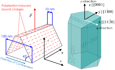
Spontaneous polarization, along induces a net negative polarization charge (in case of Ga-polar GaN) of density , where is the unit vector normal to the surface, on the inclined facades of a wedge shaped wall structure, as shown schematically in figure 1. In case of n-type GaN nanowalls, polarization charges on the side facades can create a repulsive force to the conduction band electrons resulting in a confinement in the central vertical (110) plane of the nanowalldeb . Electron movement is restricted along [110] direction, which is regarded here as x-axis.
Conduction band minimum for wurtzite(WZ) GaN remains spin degenerate even after considering the effects of crystal field and SOCGaN_without_SOC . As a result, the eigenstates, which arises due to the confinement are doubly degenerate at . Here, stands for two dimensional wavevector and can be expressed as . Lack of inversion symmetry in the WZ lattice results in a dependent spin-orbit term in the Hamiltonian, which can be expressed as01_spin ; 02_spin ; 04_spin ; 05_spin ; spin_bub ; jena :
| (1) |
Where determines the strength of the -linear Rashba like contribution. This term arises in bulk (even in the absence of structural inversion asymmetry) as a result of the built-in electric field due to spontaneous polarization02_spin . and are the Dresselhaus parameters associated with the -terms. In case of a 2DEG confined along [110] direction (x-axis), one can get an expression for for the conduction band electrons by replacing , terms in Eq.( 1) by their expectation valueswinkler1 ; winkler2 ; chang . Note that for bound eigenstates. can thus be expressed as,
| (2) |
can also be expressed as: , where is a vector representing the wave-vector dependent effective magnetic field and is the electron-spin. In case of bulk WZ-GaN, lies in plane [Eq.( 1)] and its orientation is decided by the magnitude of and . Interestingly, when 2DEG is confined in (110)-plane, no matter how is oriented in the -plane, the effective magnetic field is always along (+ or -) direction. However, the magnitude of the field depends upon the - and - components of . Below we will see that it has a remarkable consequence on the DP spin relaxation properties of electrons confined in the (110)-plane of the c-oriented wedge shaped GaN nanowall.
The DP spin relaxation equation for the density, of the spin projected along (where, ) can be written asfabian2 ; Averkiev ; long_spin_life =, where , are the Fermi distribution functions for electrons with spin , =, the spin independent momentum scattering rate between and , the angle between the initial and final wave vectors, the box normalization factor for the free part of the wave function of the confined electrons and =. It can be shown that supp , which implies that the DP mechanism does not alter the spin projection along meaning the relaxation time for component of spin is infinite. This can also be understood from the following perspective. Since always commutes with , remains a good quantum number irrespective of the direction and magnitude of . Note that the statement is valid when all other effects which can cause a spin mixing are neglected. Our calculations further show that the relaxation times for and spin components, which follow =- [], are the same and can be expressed assupp =, where =, =, and = are material dependent constants.
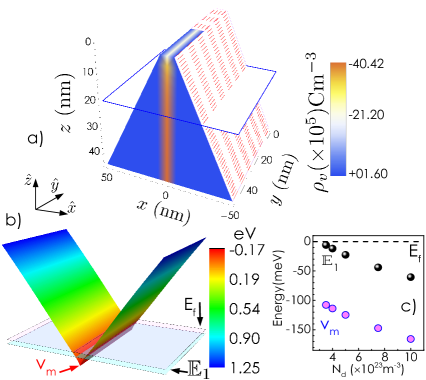
As a test case, we have considered a wedge-shaped c-oriented WZ-GaN nanowall with a background donor concentration (=) of m-3 and dimensions as shown in figure 1. The volumetric charge density and the conduction band minimum, have been obtained by solving two dimensional (2D)-Poisson’s equation with appropriate boundary as well as charge neutrality conditions as described in refdeb . Note that symmetry of the problem ensures that and are invariant along -axis. is shown in Fig. 2(a). One dimensional Schrödinger equations for at different positions are solved to obtain eigenfunctions and energy eigenvalues. These calculations are carried out at 10 K. Figure 2(b) shows the conduction band profile [] at a depth of 20 nm from the tip. Evidently, the central part of the profile goes below the Fermi surface (), forming a trench that extends along the -direction. denotes the first energy eigenstate of the quantum well at that depth. We have extended the calculation for several other values. In panel (c) the depth of the well (v) with respect to the Fermi energy and obtained at =20 nm are plotted as a function of . Evidently, both the quantities decrease monotonically with increasing donor concentration. It should be mentioned that the range of the donor concentration is chosen in a way that only one eigenstate exists around the Fermi level, at that depth from the wall apex. Henceforth, we have shown the calculations only for the electrons lying at a depth of 20 nm from the tip of the wall.
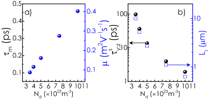
Next, we calculate momentum relaxation time, of the quantum confined electrons limited by the neutral donor scattering, which plays the most significant role in deciding the electron mobility at low temperatures in this systemdeb . Variation of and mobility () (in right -ordinate) with is plotted in figure 3(a), which clearly shows an increase of with the donor concentration. The effect can be attributed to the increasing separation between and with . Increase of the separation leads to the enhancement of electron’s kinetic energy, which results in the lowering of the scattering cross-section. Relaxation time for and components of spin as a function of is shown in figure 3(b). As expected, the spin relaxation time decreases as increases. It should be noted that comes out to be 100 ps for the nanowall with cm-3. Interestingly, a few factor change in donor density alters the spin relaxation time by about two orders of magnitude. The spin coherence length, = , where is the Fermi velocity, is also plotted as a function of in the same panel. Note that for the lowest donor concentration comes out to be as high as 10 m. As obtained earlier, the spin coherence time () for the spin projected along -direction is infinite as far as DP mechanism is concerned. Relaxation of the spin projected along -direction is thus governed mainly by EY mechanism. One can estimate EY spin relaxation time from , which comes out to be of the order of a few soptical_orientation ; bubPRB (though the relation is strictly valid for cubic GaN).
One way to manipulate spin transport in this system is to control the carrier concentration in the channel through gate bias. The idea is that with increasing carrier concentration, kinetic energy of the electrons around the Fermi level increases. This, in turn, can change both the electron mobility and the spin relaxation time. In order to calculate these changes, one needs to incorporate the effect of gate voltage in the solution of Poisson equation. Gate contact and the semiconducting channel together form a capacitor [see figure 4(a)]. When source and drain electrodes are grounded and a positive(negative) gate voltage is applied, some amount of electrons are pumped(removed) into(from) the channel by the power supply. Since the semiconductor is no longer charge neutral, the Poisson’s equation has to be solved by satisfying appropriate positive to negative charge ratio condition (instead of satisfying charge neutrality) to obtain the profiles. Total positive to negative charge ratio () should be less(greater) than 1 when sufficiently positive(negative) gate voltages are applied. As shown in Fig. 4(b), the gap between and decreases as increases. Note that when is sufficiently less than unity [high gate voltages], more than one bound states are formed below the Fermi level.
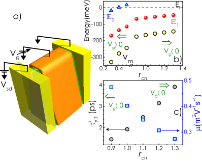
Variation of and with are shown in Fig. 4(c). As the gap between and decreases with the increase of , reduces while enhances.
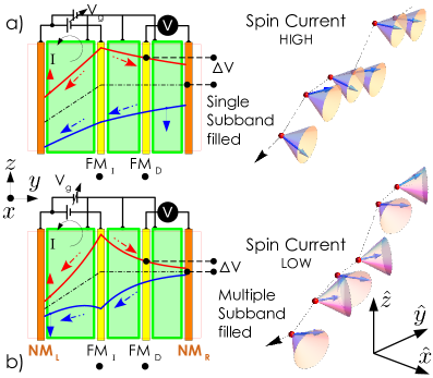
As shown earlier, spin component along x-direction does not relax in this system as DP process is completely switched-off for this spin projection. This assertion is strictly valid when only a single subband is occupied. When more than one eigenstates are formed below the Fermi level, DP relaxation is activated even for the x projection of spin as in this case, wavefunction for the electrons near the Fermi level becomes a linear superposition of multiple eigenstates. In such a situation, is no longer equal to zeromultibandDP . Finite value of results in a non-zero component of . Thus, does not commute with any of the spin components resulting in a finite relaxation time for the spin density as well. This property can be exploited to envisage a novel type of spin-transistor. A schematic of such a device is shown in figure 5(a). In this nonlocal spin valve (spin-transistor) device, the pair of contacts in the middle are made of ferromagnetic metals (FM), while the contacts on edges are nonmagnetic (NM). The FM contact on left is the spin injector (FM) while the other works as the detector (FM). Consider the case when both FM and FM are coupled to spin up (with respect to x axis) electrons. At an adequately high negative gate voltage, when only one subband is filled, the x-polarized spin up current injected from FM reaches the detector electrode without losing its coherence. As a result, the spin current through the channel is high and ‘spin-resolved charge voltage’ measured between FM and NM will be sufficiently high. Upon application of a large positive gate bias, more than one subbands are filled. At this condition, the direction of the effective magnetic field (), which is the Larmor precession axis of electron spin, get randomized due to successive scattering events. As a result, the x projection of spin also relaxes. This should result in a rapid decay of pure spin current in the channel between FM and FM, as depicted in figure 5(b). The device can thus act as a spin-transistor. Note that the nature of quantum confinement in this system is such that it preserves the symmetry between conduction and valence band everywhere irrespective of the fact whether the nanowedge is geometrically symmetric or not. This results in the suppression of the Rashba effect, which comes as an added advantage in maintaining spin coherence of electrons in this system. Note that, this novel 2DEG system is substantially different from the 2DEG, formed at the heterojunction of a-directional GaN/AlGaN as discussed in supplementary informationsupp .
Spin relaxation of electrons in a 2DEG formed at the central vertical plane of a c-oriented wedge-shaped WZ-GaN nanowall is theoretically investigated. It has been found that the component of spin projected in the plane of the confinement relaxes through DP mechanism with a time-scale of a few tens of picoseconds everywhere in the channel, while the spin component along the direction of confinement never relaxes through DP process in a part of the channel, where the Fermi-level occupies only one subband. However, by applying appropriate positive gate bias, electron concentration in the well can be sufficiently enhanced, which can bring in more than one subbands below the Fermi-level in most of the channel. At this situation, DP relaxation mechanism is switched-on also for the spin component along the confinement direction. One can envisage a novel spin-transistor, where this property can be exploited to electrically manipulate spin current.
We acknowledge the financial support by Department of Science and Technology, Government of India under the project Code:CRG/2018/001343.
References
- [1] Supriyo Datta and Biswajit Das. Electronic analog of the electro-optic modulator. Appl. Phys. Lett., 56:665, 1990.
- [2] G. Salis, Y. Kato, K. Ensslin, D. C. Driscoll, A. C. Gossard, and D. D. Awschalom. Electrical control of spin coherence in semiconductor nanostructures. Nature, 414:619–622, 2001.
- [3] A. Hernández-Mínguez, K. Biermann, R. Hey, and P. V. Santos. Electric control of spin transport in GaAs (111) quantum wells. Phys. Rev. B, 94:125311, 2016.
- [4] Felix Trier, Diogo C Vaz, Pierre Bruneel, Paul Noël, Albert Fert, Laurent Vila, Jean-Philippe Attané, Agnès Barthélémy, Marc Gabay, Henri Jaffrès, et al. Electric-field control of spin current generation and detection in ferromagnet-free SrTiO3-based nanodevices. Nano Letters, 2019.
- [5] Debdeep Jena. Spin scattering by dislocations in iii-v semiconductors. Phys. Rev. B, 70:245203, 2004.
- [6] M.I. Dyakonov. Spin Physics in Semiconductors, volume 157. Springer Series in Solid-State Sciences, 2008.
- [7] S. Ghosh, V. Sih, W. H. Lau, D. D. Awschalom, S.-Y. Bae, S. Wang, S. Vaidya, and G. Chapline. Room-temperature spin coherence in zno. Applied Physics Letters, 86(23):232507, 2005.
- [8] Hyun Kum, Junseok Heo, Shafat Jahangir, Animesh Banerjee, Wei Guo, and Pallab Bhattacharya. Room temperature single gan nanowire spin valves with feco/mgo tunnel contacts. Applied Physics Letters, 100(18):182407, 2012.
- [9] J. H. Buß, J. Rudolph, F. Natali, F. Semond, and D. Hägele. Temperature dependence of electron spin relaxation in bulk GaN. Phys. Rev. B, 81:155216, 2010.
- [10] Jörg Rudolph, Jan Heye Buß, and Daniel Hägele. Electron spin dynamics in GaN. physica status solidi (b), 251:1850, 2014.
- [11] V. I. Litvinov. Polarization-induced rashba spin-orbit coupling in structurally symmetric III-nitride quantum wells. Appl. Phys. Lett., 89:222108, 2006.
- [12] J. H. Buß, S. Fernández-Garrido, O. Brandt, D. Hägele, and J. Rudolph. Electron spin dynamics in mesoscopic GaN nanowires. Appl. Phys. Lett., 114:092406, 2019.
- [13] J. Besbas, A. Gadalla, M. Gallart, O. Crégut, B. Hönerlage, P. Gilliot, E. Feltin, J.-F. Carlin, R. Butté, and N. Grandjean. Spin relaxation of free excitons in narrow quantum wells. Phys. Rev. B, 82:195302, 2010.
- [14] Tae-Eon Park, Youn Ho Park, Jong-Min Lee, Sung Wook Kim, Hee Gyum Park, Byoung-Chul Min, Hyung-jun Kim, Hyun Cheol Koo, Heon-Jin Choi, Suk Hee Han, Mark Johnson, and Joonyeon Chang. Large spin accumulation and crystallographic dependence of spin transport in single crystal gallium nitride nanowires. Nature Communications, 8:15722, 2017.
- [15] Hyun Kum, Junseok Heo, Shafat Jahangir, Animesh Banerjee, Wei Guo, and Pallab Bhattacharya. Room temperature single GaN nanowire spin valves with FeCo/MgO tunnel contacts. Applied Physics Letters, 100:182407, 2012.
- [16] S. Deb, H. P. Bhasker, Varun Thakur, S. M. Shivaprasad, and S. Dhar. Polarization induced two dimensional confinement of carriers in wedge shaped polar semiconductors. Sci. Rep., 6:26429, 2016.
- [17] H. P. Bhasker, S. Dhar, A. Sain, Manoj Kesaria, and S. M. Shivaprasad. High electron mobility through the edge states in random networks of c-axis oriented wedge-shaped GaN nanowalls grown by molecular beam epitaxy. Appl. Phys. Lett., 101:132109, 2012.
- [18] H P Bhasker, Varun Thakur, S M Shivaprasad, and S Dhar. Quantum coherence of electrons in random networks of c-axis oriented wedge-shaped GaN nanowalls grown by molecular beam epitaxy. J. Phys. D: Appl. Phys., 48:255302, 2015.
- [19] H.P. Bhasker, Varun Thakur, S.M. Shivaprasad, and S. Dhar. Role of quantum confinement in giving rise to high electron mobility in GaN nanowall networks. Solid State Commun., 220:72, 2015.
- [20] H. P. Bhasker, Varun Thakur, Manoj Kesaria, S. M. Shivaprasad, and S. Dhar. Transport and optical properties of c-axis oriented wedge shaped GaN nanowall network grown by molecular beam epitaxy. AIP Conf. Proc., 1583:252, 2014.
- [21] A. K. Jain, H. Chakraborti, B. P. Joshi, B. Pal, M. Monish, S. M. Shivaprasad, S. Dhar, and K. Das Gupta. Effect of invasive probes on measurement of magneto-transport in macroscopic samples: A gallium nitride case study. J. Appl. Phys., 126:085706, 2019.
- [22] Himadri Chakraborti, Swarup Deb, Rüdiger Schott, Varun Thakur, Abhijit Chatterjee, Santosh Yadav, Rajendra K Saroj, Andreas Wieck, S M Shivaprasad, K Das Gupta, and S Dhar. Coherent transmission of superconducting carriers through a 2 m polar semiconductor. Superconductor Science and Technology, 31(8):085007, 2018.
- [23] Igor Žutić, Jaroslav Fabian, and S. Das Sarma. Spintronics: Fundamentals and applications. Rev. Mod. Phys., 76:323–410, Apr 2004.
- [24] Jaroslav Fabian, Alex Matos-Abiague, Christian Ertler, Peter Stano, and Igor Žutić. Semiconductor spintronics. Acta Physica Slovaca. Reviews and Tutorials, 57(4-5), Aug 2007.
- [25] Swarup Deb and Subhabrata Dhar. Wedge-shaped GaN nanowalls: A potential candidate for two-dimensional electronics and spintronics. Spin, 08:1840003, 2018.
- [26] Pojen Chuang, Sheng-Chin Ho, L. W. Smith, F. Sfigakis, M. Pepper, Chin-Hung Chen, Ju-Chun Fan, J. P. Griffiths, I. Farrer, H. E. Beere, G. A. C. Jones, D. A. Ritchie, and Tse-Ming Chen. All-electric all-semiconductor spin field-effect transistors. Nature Nanotechnology, 10:35–39, 2015.
- [27] Youn Ho Park, Jun Woo Choi, Hyung-jun Kim, Joonyeon Chang, Suk Hee Han, Heon-Jin Choi, and Hyun Cheol Koo.
- [28] C. Lu, H. C. Schneider, and M. W. Wu. Electron spin relaxation in n-type InAs quantum wires. Journal of Applied Physics, 106:073703, 2009.
- [29] Xin he Jiang, Jun jie Shi, Min Zhang, Hong xia Zhong, Pu Huang, Yi min Ding, Tong jun Yu, Bo Shen, Jing Lu, and Xihua Wang. Enhancement of TE polarized light extraction efficiency in nanoscale AlNm/GaNn() superlattice substitution for Al-rich AlGaN disorder alloy: ultra-thin GaN layer modulation. New Journal of Physics, 16(11):113065, 2014.
- [30] J. Y. Fu and M. W. Wu. Spin-orbit coupling in bulk ZnO and GaN. J. Appl. Phys., 104:093712, 2008.
- [31] J. Kainz, U. Rössler, and R. Winkler. Anisotropic spin-splitting and spin-relaxation in asymmetric zinc blende semiconductor quantum structures. Phys. Rev. B, 68:075322, 2003.
- [32] J. Kainz, U. Rössler, and R. Winkler. Temperature dependence of dyakonov-perel spin relaxation in zinc-blende semiconductor quantum structures. Phys. Rev. B, 70:195322, 2004.
- [33] X. Cartoixà, D. Z.-Y. Ting, and Y.-C. Chang. Suppression of the D’yakonov-Perel’ spin-relaxation mechanism for all spin components in [111] zincblende quantum wells. Phys. Rev. B, 71:045313, 2005.
- [34] N S Averkiev, L E Golub, and M Willander. Spin relaxation anisotropy in two-dimensional semiconductor systems. Journal of Physics: Condensed Matter, 14:R271, 2002.
- [35] N. J. Harmon, W. O. Putikka, and Robert Joynt. Prediction of extremely long mobile electron spin lifetimes at room temperature in wurtzite semiconductor quantum wells. Appl. Phys. Lett., 98:073108, 2011.
- [36] Supplementary information. S1. Detailed derivation of spin relaxation time for x, y and z projections of spin. S2. Comparison of the present case with AlGaN/GaN heterojunction 2DEG.
- [37] G.E. Pikus and A.N. Titkov. Optical Orientation, volume 8. edited by F. Meier, B.P. Zakharchenya North-Holland Physics Publishing, Elsevier Science Publishers, 1984.
- [38] J. H. Buß, T. Schupp, D. J. As, O. Brandt, D. Hägele, and J. Rudolph. Electron spin dynamics in cubic gan. Phys. Rev. B, 94:235202, Dec 2016.
- [39] J. Kainz, U. Rössler, and R. Winkler. Temperature dependence of dyakonov-perel spin relaxation in zinc-blende semiconductor quantum structures. Phys. Rev. B, 70:195322, 2004.
- [40] Yasuhiro Isobe, Hiromichi Ikki, Tatsuyuki Sakakibara, Motoaki Iwaya, Tetsuya Takeuchi, Satoshi Kamiyama, Isamu Akasaki, Takayuki Sugiyama, Hiroshi Amano, Mamoru Imade, Yasuo Kitaoka, and Yusuke Mori. Nonpolara-plane AlGaN/GaN heterostructure field-effect transistors grown on freestanding GaN substrate. Applied Physics Express, 4:064102, 2011.
- [41] Takashi Matsuda and Kanji Yoh. Enhancement of spin–orbit interaction by bandgap engineering in inas-based heterostructures. J. Electron. Mater., 37:1806, 2008.
- [42] P. S. Eldridge, W. J. H. Leyland, P. G. Lagoudakis, R. T. Harley, R. T. Phillips, R. Winkler, M. Henini, and D. Taylor. Rashba spin-splitting of electrons in asymmetric quantum wells. Physical Review B, 82:045317, 2010.
- [43] R. Lassnig. kp theory, effective-mass approach, and spin splitting for two-dimensional electrons in GaAs-GaAlAs heterostructures. Phys. Rev. B, 31:8076, 1985.
- [44] P. S. Eldridge, W. J. H. Leyland, J. D. Mar, P. G. Lagoudakis, R. Winkler, O. Z. Karimov, M. Henini, D. Taylor, R. T. Phillips, and R. T. Harley. Rashba conduction band spin-splitting for asymmetric quantum well potentials. Journal of Superconductivity and Novel Magnetism, 23:157, 2009.
Supplementary Information
Spin transport in polarization induced two dimensional confinement of carriers in wedge shaped c-GaN nanowalls
Swarup Deb, Subhabrata Dhar
Department of Physics, Indian Institute of Technology Bombay, Powai, Mumbai-400076, India
S1. Derivation of spin relaxation time
In order to calculate the DP spin relaxation time we follow the formalism described by N. S. Averkiev et al.[34] and J. Fabian et al.[24]. The DP relaxation rate for spin density, projected along () can be written as[35]:
| (3) |
where, , are the Fermi distribution functions for electrons with spin . are the relaxation times[39, 35], which can be expressed as:
| (4) |
where, the spin independent momentum scattering rate between and , the angle between the initial and final wave vectors, the box normalization factor for the free part of the wave function of the confined electrons. are the Fourier harmonics of spin-orbit Hamiltonian:
| (5) |
Because of the presence of linear and cubic terms of in , survives only for .
It can be shown that:
| (6) | |||||
| (7) | |||||
For, the trace, in equation (3) takes the form:
| (8) |
In the above relation, the dependent prefactors are dropped for simplicity. We have also taken the advantage of the fact that in such quantum confined system get coupled to , only. The Pauli matrices follow the commutation relation , is the Levi-Civita tensor. Using this relation the trace can be evaluated as:
| (9) | |||||
Again, only if but in that case or are 0 and vice versa. Thus the term in the numerator of equation (3) becomes 0 for , leading to
| (10) |
Derivation of and is slightly tedious. The trace in the numerator of equation (3) has to be evaluated for all possible combination of , and . As an example we evaluate the terms for in table 1. Thus has been replaced with .
| n | j=x | j=y | j=z |
| +3 | |||
| = 0 | = | = 0 | |
| +1 | |||
| = 0 | = | = 0 | |
| -1 | |||
| = 0 | = | = 0 | |
| -3 | |||
| = 0 | = | = 0 |
can also be evaluated in a similar fashion. It is important to note that only depends on the spin projection, . The same hold for the z component also. Thus one can write the spin relaxation time of y and z components as:
| (11) |
Following reference[34], we write and as
| (12) |
Following parameter values are used during numerical calculation: =9.0 meVÅ; =3.959; =0.32 eVÅ3[10]
S2. Spin dynamics:a-plane 2DEG in a AlGaN/GaN Heterojunction versus a-plane 2DEG in -oriented GaN nanowedge
At a first glance, 2D electron gas confined in a-plane of AlGaN/GaN[40] appears very similar to the present case of the 2DEG formed in a -oriented wedge shaped GaN nanowall structure. However, unlike the present case, such a heterojunction lacks spatial inversion symmetry(SIA) leading to the existence of a net electric field. This assertion requires a more careful discussion.
In a quantum confined system, the effective electric field can be quantified by the expectation value of the field i.e. . Where, is the conduction band energy profile in real space and is the electron charge. Using the identities from Ehrenfest theorem:
| (13) | |||||
| (14) |
For a bound eigen state, time derivative of = 0 and hence the effective electric field is also zero. This was first pointed out by T. Ando[41, 42] who argued that the spin splitting of conduction band must be negligibly small in such system. Later, Lassnig[43] showed that Rashba field in such quantum well system will be proportional to the average electric field of valence band seen by the conduction band electrons i.e. . Where, denotes the wave-function for the electrons at the conduction band edge and is the valence band edge profile. In a a-plane 2DEG of AlGaN/GaN heterojunction, the band offset breaks the symmetry between the conduction and valence band across the junction. As a result, does not vanish for a bound state while does. Due to Rashba effect, this average field gives rise to an effective magnetic field acting perpendicular to [44, 42] and becomes
| (15) |
Clearly, does not commute with any of the ’s. Spin density thus follows a different dynamics than in the present case. It should be noted that in case of the a-plane 2DEG in c-oriented wedge shaped GaN nanowalls, both ==0 as the symmetry between the conduction and valence band across the junction is intact. This is true even when the shape of the wedge is asymmetric. Therefore, the spin dynamics remains to be the same for both asymmetric and symmetric nanowedges.