Development of highly sensitive nanoscale transition edge sensors for gigahertz astronomy and dark matter search
Abstract
Terahertz and sub-terahertz band detection has a key role both in fundamental interactions physics and technological applications, such as medical imaging, industrial quality control and homeland security. In particular, transition edge sensors (TESs) and kinetic inductance detectors (KIDs) are the most employed bolometers and calorimeters in the THz and sub-THz band for astrophysics and astroparticles research. Here, we present the electronic, thermal and spectral characterization of an aluminum/copper bilayer sensing structure that, thanks to its thermal properties and a simple miniaturized design, could be considered a perfect candidate to realize an extremely sensitive class of nanoscale TES (nano-TES) for the giga-therahertz band. Indeed, thanks to the reduced dimensionality of the active region and the efficient Andreev mirror (AM) heat confinement, our devices are predicted to reach state-of-the-art TES performance. In particular, as a bolometer the nano-TES is expected to have a noise equivalent power (NEP) of W/ and a relaxation time of ns for the sub-THz band, typical of cosmic microwave background studies. When operated as single-photon sensor, the devices are expected to show a remarkable frequency resolution of 100 GHz, pointing towards the necessary energy sensitivity requested in laboratory axion search experiments. Finally, different multiplexing schemes are proposed and sized for imaging applications.
I Introduction
In the last decade, astronomy and astrophysics have broadened their interest towards low energy phenomena, such as cosmic microwave background (CMB) Sironi , atomic vibrations in galaxy clusters Villaescusa-Navarro , and new particles in dark matter Redondo . To obtain physical insight of these phenomena, the detection of faint signals in the micro- (terahertz) and sub-millimeter (gigahertz) spectral range plays a fundamental role. To this end, the key ingredient is the development of new ultrasensitive bolometers and single-photon detectors, i.e., calorimeters. On the one hand, the temperature and polarization maps of the CMB fluctuations Seljak ; Kamionkowski and the detection of polarized radiation due to the hydrogen atom emission in the galaxy clusters Armus are the main astronomy applications for gigahertz (GHz) and terahertz (THz) bolometers. On the other hand, low frequency calorimeters could play a fundamental role in axions search Ringwald , one of the principal candidates for the dark matter. Axions are very weakly interacting particles with small mass ( meV) thus impossible to be revealed by means of colliders. Therefore, light-shining-through-wall (LSW) experiments have been proposed to generate axion-like particles (ALP) in the laboratory Spagnolo , differently from experiments focused on space surveys, such as CAST Arik and IAXO Armengaud .
Nowadays, the most employed detectors in the THz energy band are the superconducting sensors, such as transition edge sensors (TESs) (Irwin1995a, ; Irwin2006, ; Karasik, ) and kinetic inductance detectors (KIDs) Monfardini , for their high sensitivity, robustness and mature technology. The state-of-the-art of these detectors in bolometric operation shows a noise equivalent power (NEP) of for TESs Khosropanah with large active area ( 100 ), and for KIDs Visser . More sensitive and efficient superconducting detectors have been proposed and realized by taking advantage of device miniaturization Wei and Josephson effect. For instance, detectors based on superconductor/normal metal/superconductor (SNS) junctions showed a NEP of the order of Kokkoniemi , cold electron bolometers showed a kuzmin2019 , devices based on the temperature-to-phase conversion (TPC) are expected to provide Virtanen , while a fully superconducting tunable Josephson escape sensor (JES) showed a record intrinsic NEP as low as Paolucci .
To push the TES technology towards lower values of NEP with the possibility to detect single photons in the GHz band Alesini , a strong reduction of the thermal exchange mechanisms of the active region, i.e., the portion of the device transitioning to the normal-state when radiation is absorbed, is necessary Bergmann . To this end, we envision a nanoscale TES (nano-TES) exploiting a simple and sturdy miniaturized design together with the Andreev mirrors (AM) effect andreev to thermally isolate the sensor active region. Here, we present and experimentally characterize the active region of the nano-TES structures by an electrical and a thermal points of view. For simplicity, we will adopt the notation nano-TES to indicate the structures analyzed in this paper. Indeed, operating in the bolometer configuration our nano-TESs would reach a total noise equivalent power () of , while as calorimeters they are expected to reach a resolving power () of in sub-THz band. Their measured thermal and electrical performance are several orders of magnitude better than devices with identical dimensions but without the Andreev mirrors heat constrictions. Finally, we propose and size two possible multiplexing circuits in frequency domain (FDM) and microwave resonators (MR) as readout for a nano-TES array enabling the realization of multi-pixel cameras. In addition to gigahertz astronomy and particle physics, the nano-TES could find applications for medical imaging Sun , industrial quality controls Ellrich and security Rogalski .
This paper is organized as follows. Section II reports the simple fabrication of the nano-TES and of a secondary device used to extract all the parameters of the active region. Section III describes the electrical properties of the nano-TES. The spectral and thermal characterization of the active region are resumed in Sec. IV and V, respectively. The expected nano-TES performance as a bolometer and a calorimeter deduced from the experimental data are reported in Sec. VI together with the comparison of a TES of identical materials and dimensions but not equipped with AM. Finally, Sec. VII covers possible multiplexing readout circuits to design multi-pixel cameras.
II Devices fabrication
The experiments discussed in this paper are performed thanks to two different device architectures: the nano-TES and a secondary device (SD). Measurements on the nano-TES provided the active region resistance versus temperature characterization, , the active region critical and retrapping current, and the critical temperature . Instead, the active region spectral and thermal properties have been obtained by the experiments performed on the SD.
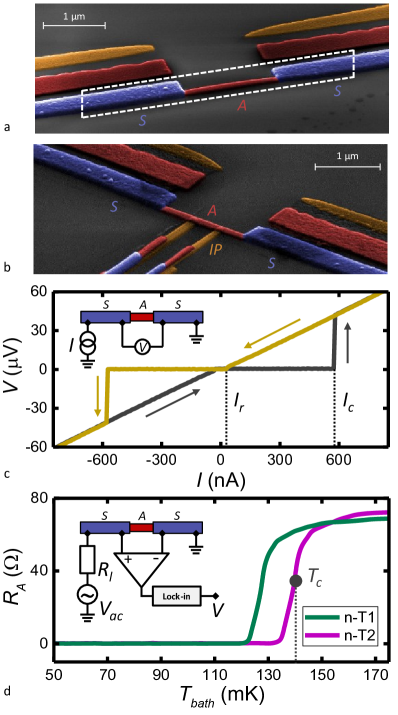
The false-color scanning electron microscope (SEM) pictures of a typical nano-TES and SD are shown in Fig. 1-a and -b, respectively. The nano-TES, highlighted by the dashed white box in Fig. 1-a, consists in a 1.5 m-long, 100 nm-wide and 25 nm-thick Al/Cu bilayer nanowire-like active region (red), which is sandwiched between the Al electrodes (blue). Since the superconducting gap of the Al layer is higher than that of the Al/Cu bilayer (due to inverse proximity effect tinkham ), the electrodes act as AM for the active region, leading to the advantages discussed in Sec. V. The same nano-TES structure is visible in the SD (see Fig. 1-b) with the addition of two oxidized Al probes (yellow) lying under the active region forming two tunnel Josephson junctions (JJs) Giazotto . These two Al probes allow to characterize both the energy gap and the thermal properties of the active region.
Both the nano-TES and the SD were realised during the same fabrication process, ensuring the homogeneity of their properties. They were fabricated by electron-beam lithography (EBL) and 3-angles shadow mask evaporation of metals onto a silicon wafer covered with 300 nm of thermally grown SiO2. The evaporation was performed in an ultra-high vacuum electron-beam evaporator with base pressure of about Torr. By referring to the color code of Fig 1-a and -b, the fist Al layer (yellow) with thickness 13 nm was evaporated at an angle of -40∘ and then oxidized by exposition to 200 mTorr of O2 for 5 minutes to obtain the tunnel probes in the SD. In a second step, the Al/Cu bilayer (red) was evaporated at an angle of to form the active region with partial thicknesses nm and nm for the aluminum and copper layer, respectively. Finally, a second Al layer (blue) of thickness 40 nm was evaporated at an angle of to obtain the AM electrodes.
The notation A, S, P and I will be used to indicate the Al/Cu active region, the Al electrodes, the Al probes and the probes insulating barrier, respectively. The nano-TES measurements have been performed on two different devices, n-T1 and n-T2. All the following experiments have been performed in a 3He-4He dilution refrigerator with bath temperature ranging from 20 mK to 250 mK.
III Nano-TES electrical properties
The four-terminal voltage-current characteristics of n-T1 are shown in Fig. 1-c at mK for a positive (grey line) and a negative (yellow line) current slope. The electrical measurement setup is schematized in the inset. Here, the normal and the superconducting state are recognizable by the linearly growing and the flat behaviour of the traces, respectively. The transition occurs at the critical current nA, whereas the occurs at the retrapping current 27 nA courtois . The normal-state resistance is obtained by the slope of the and gets value , while it is obviously zero in the . This change of has a key role in the operation mechanism of a TES detector Irwin1995a (see Sec. VII for further details).
The temperature dependence of is shown in Fig. 1-d for n-T1 (green line) and n-T2 (purple line). The inset shows the experimental setup. The AC current bias is produced by applying a voltage at 13.33 Hz to a load resistance k () in order to obtain nA independent from . The voltage drop across the nano-TES is measured as a function of via a voltage pre-amplifier connected to a lock-in amplifier. By rising , the resistance changes from zero to its normal-state value, by following an edge transition behaviour. The nano-TES critical temperature is defined as the temperature corresponding to half of the normal-state resistance (grey point for n-T2 in Fig. 1-d). Thus, we have mK and for n-T1 and n-T2, respectively.
IV Spectral characterization of the active region
For , the energy gap of a superconductor [] is temperature independent and equals its zero-temperature value tinkham . For higher values of temperature, decreases monotonically and finally disappears at . Typically, aluminum thin films show a higher than the bulk Al value ( K) cochran . Therefore, the superconducting gaps of S and P, and , are temperature independent up to at least 500 mK, thus preserving their zero-temperature values ( and ). By contrast, due to inverse proximity effect tinkham , superconductivity in is strongly suppressed. In fact, our resistance versus temperature experiments showed a value mK (see Fig. 1-d), thus enabling the possibility to independently determine both and .
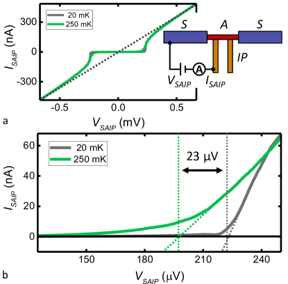
To this end, the characteristics of a SAIP JJ were measured at base temperature and just above , as reported in Fig. 2-a with the grey and the green line, respectively. The experimental setup of the measurements is schematically shown in the inset of the panel. At base temperature, the JJ switches to the -state when the voltage bias reaches Giazotto , where is the elementary charge. Instead, at mK the transition occurs at , since A is in the -state. The tunnel resistance of the JJ is given by the slope of the characteristic in the linear region, as highlighted by the black dotted line, and gets value k.
In order to provide a precise evaluation of the energy gaps, the characteristics are zoomed around the switching points acquired for positive voltage bias, as shown in Fig. 2-b. The measurement at mK (green line) indicates a value of the zero-temperature superconducting gap of the aluminum probes eV, corresponding to a critical temperature K. Note that , since electrodes and probes thickness are similar meservey , thus K as well. Instead, the difference between the results obtained at 20 mK and 250 mK leads to eV corresponding to a critical temperature mK, in good agreement with the data reported in Fig. 1-d.
Importantly, the superconducting gap of A is constant along the out-of-plane axis (i.e., the sample thickness), because the bilayer is within the Cooper limit DeGennes1964 ; Kogan1982 . In fact, the aluminum thin film follows nm (where m2s-1 is the diffusion constant of Al and eV is the superconducting energy gap), while the copper layer respects nm (where m2s-1 is the copper diffusion constant and the temperature is chosen mK thus higher than the nano-TES operation value). Furthermore, the active region is much thinner than its superconducting coherence length, that is nm, where is the electron charge, while J-1m-3 and J-1m-3 are the density of states (s) at the Fermi level of aluminum and copper, respectively.

V Thermal characterization of the active region
Energy exchange has a key role in determining the nano-TES performance, such as sensitivity and response time, since the increase of the electronic temperature due to the incident radiation strongly depends on the capability of maximizing the thermal confinement. The scope of this section is to study the most prominent heat exchange mechanisms in the active region of the nano-TES for typical operating conditions.
Metallic elements in mesoscopic devices at sub-kelvin temperatures show weak coupling between the electron and the phonon thermal subsystems Giazotto , which can lead to , where and are the electron and phonon temperature, respectively. Due to the thickness of the films lower than the phonon wavelength and vanishing Kapitza resistance, the device phonons are thermally anchored to the substrate () wellstood , so that the temperature of both systems can be considered as a parameter set via the refrigerator temperature . The geometry of our device also guarantees electronic temperature of the superconducting electrodes and the tunnel probes equal to the phonon temperature, that is . By contrast, the electronic temperature is the fundamental thermal variable in the nano-TES operation mechanism. In general, the value of results from the balance between the main thermal exchange channels of A. In our case:
| (1) |
where is the power injected, is the electron-phonon relaxation, represents the heat losses through and is the energy diffusion by an probe. Note that the electron-photon interaction contribution has not been considered in the model, since it is negligibly small with comparison to the other thermal channels bosisio .
The use of with energy gap much larger than can ensure negligible heat out-diffusion from to . Indeed, the normalised DOS of a superconductor reads Giazotto :
| (2) |
Thus, the zero-temperature energy-dependent DOS of S and A are calculated by inserting the measured values of and . The resulting functions are shown in Fig. 3-a with the blue and the red line, respectively. The thermally excited quasi-particles in A do not find available states towards S, thus the resistance for heat diffusion exponentially rises by decreasing the bath temperature andreev . In particular, at the superconducting leads act as AM, namely as perfect barriers for energy diffusion (). In addition, the big difference between the two superconducting gap ensures that the nano-TES superconducting to dissipative transition affects only , leading to a better control in the resistance change and a small overheating of the detector.
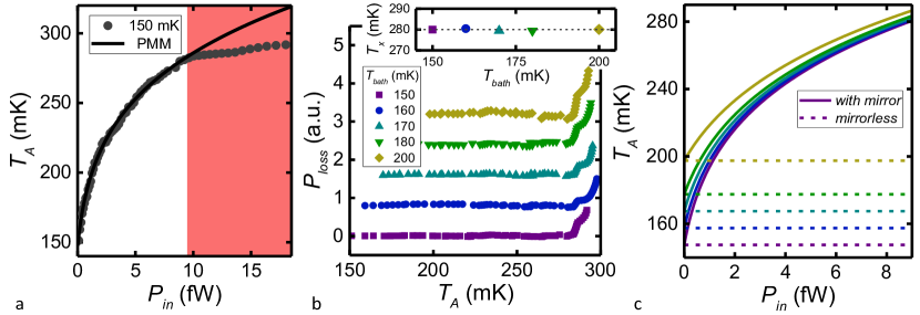
The experimental setup employed to perform the thermal study of A is schematically shown in Fig. 3-b: the left SAIP junction was current-biased (at ) to operate as thermometer, whereas the right JJ was voltage-biased (at ) to work as heater Giazotto . The thermometer has been calibrated by varying and measuring at pA and V, as reported in Fig. 3-c. The bath temperature ranges from mK to mK, so , i.e. A is in the normal state, whereas . In this normal metal ()/insulator/superconductor () JJ, the characteristics depends only on the electronic temperature of the normal metal Giazotto . Therefore, the values of directly reflect .
The heater has been calibrated by acquiring the current-to-voltage characteristic of the tunnel junction at the different values of . In particular, the injected power is given by , where the factor 0.5 stems from the fact that the heat is equally dissipated on the two sides of the junction. In this experimental configuration, the heat is generated at one side of the active region, while the thermometer is placed in the vicinity of the opposite end (see Figs. 1b and 3b). The electrons is thermalize through electron-electron interaction and electron-phonon scattering, while the heat losses through the thermometer tunnel junction is negligible compared to the other contributions (see Subsection Perfect Andreev mirrors. As a consequence, the electronic temperature in the active region varies for distances of the order of the electron-phonon coherence length Giazotto , where is the diffusion constant of the active region and s is the electron-phonon scattering time (see Section Bolometer for details). Since the length of the active region is m, we can assume that the electronic temperature in the active region is homogeneous during our experiments.
V.0.1 Perfect Andreev mirrors
Figure 3-d shows as a function of the input power acquired at mK in three different sets of measurements. The electronic temperature monotonically increases from 150 mK to mK by rising to fW. Within the experimental parameters, the inequality is always satisfied. Therefore, the perfect mirror model (PMM) can describe the data: the heat exchange between and s is fully suppressed (), i.e. A is thermally isolated from . Thus, the injected power relaxes only via electron-phonon interaction and out-diffuses through the thermometer . The resulting quasi-equilibrium equation describing the PMM reads
| (3) |
as schematically represented in Fig. 3-e.
Since is in the -state, the power exchanged via electron-phonon interaction can be written as Giazotto :
| (4) |
where is the electron-phonon thermal relaxation constant and is the volume of A. The power which flows through the thermometer JJ takes the form Giazotto
| (5) |
where is the of the superconducting probe, is the energy of the active region, and is the Fermi-Dirac distribution of A and P, respectively.
By solving Eq. (3), we fit the experimental electronic temperature of the as a function of , as shown by the black line in Fig. 3-d. Since all the other device parameters are known ( m3, k and mK), we extracted the value of the electron-phonon coupling constant of the Al/Cu bilayer W/m3K5. We notice that the PMM provides a remarkable fit of the experimental data thus describing correctly the system. The contribution of the electron-phonon relaxation is about one order of magnitude larger than the thermal losses through the thermometer tunnel junction. Therefore, the presence of the thermometer tunnel barrier as a negligible impact on the thermal experiment. Furthermore, the resulting electron-phonon relaxation constant is in good agreement with the average of W/m3K5 and W/m3K5 Giazotto , weighted with the volumes of the copper and the aluminum layer forming the active region: W/m3K5, with m-3 and m-3.
V.0.2 Low-efficiency Andreev mirrors
In order to test the AM efficiency and the limits of the PMM, we investigated the dependence of on larger values of . The PMM fails for fW (the red shaded area in Fig. 4-a), where the power loss through the S-electrodes is no longer negligible () and the resulting increase of is reduced.
The energy losses through the superconducting electrodes can be evaluated by calculating the difference between the measured necessary to produce a specific and its value estimated from the PMM. The dependence of on is shown in Fig. 4-b for different values of . For all the curves, the energy loss through the Andreev mirrors is negligible until reaching a threshold temperature . Notably, for all measurements we obtain mK (see the inset of Fig. 4-b), independently from the value of and thus . Furthermore, the energy filtering of the superconducting electrodes starts to fail for , that is in good agreement with the theoretical prediction of Andreev andreev . Finally, the staircase behavior of present at mK (see Fig. 4-b) could be due to superconducting proximity effect at the / interface. However, a complete explanation of such behavior would require further measurements and analysis.
The versus characteristics change dramatically in a mirror-less device. Indeed, in a TES based on the same structure and dimensions but without AMs, the active region extends to the entire device, i.e. it is composed by a single superconductor. Fig. 4-c shows the difference between our nano-TES (solid lines) and a TES without Andreev mirrors (dashed lines) calculated for the same values of bath temperature of our experiments. As expected, at a given value of the temperature of the active region rises more in the presence of energy filtering than in a composite device, since the main channel for thermalization, the electron-phonon coupling, linearly depends on the volume (see Eq. 4). As a consequence, the presence of Andreev mirrors promises enhanced sensitivity of the nano-TES.
VI Nano-TES Performance
This section is devoted to the prediction of the performance of our device when operated as a radiation sensor. Our study will focus on both the bolometric operation, i.e. in continuous incident radiation, and the calorimetric operation, i.e. in single photon detection. Moreover, we propose a comparison between this device and an identical one without AM.
The typical read-out circuit for a TES is schematized in Fig. 5. On the one hand, the decrease of the current flowing through the inductance due to photon absorption can be measured by means of an inductively coupled superconducting quantum interference device (SQUID) amplifier. On the other hand, the shunt resistor implements the negative electro-thermal feedback mechanism (NETF), which guarantees constant voltage bias of the nano-TES and faster heat removal after radiation absorption IrwinBook . To this end, the shunt resistor needs to satisfy the relation Irwin1995b . In the following, we will use a value m typical for SQUID amplifier-based read-out.
| n-T | |||||||
| (mK) | () | () | (W/) | (W/) | (GHz) | ||
| 100 GHz 300 GHz 1 THz | |||||||
| 1 | 128 | 6 | 0.01 | 5.2 x | 5.2 x | 100 | 1 3 10 |
| 1* | 1.1 x | 4.7 x | 2 x | 4 x 1 x 4 x | |||
| 2 | 139 | 5 | 0.2 | 6.7 x | 6.7 x | 540 | 0.18 0.55 1.8 |
| 2* | 1.5 x | 8.3 x | 1 x | 8 x 2 x 8 x |
VI.1 Bolometer
Starting from the structure and the measured parameters, we evaluate the performance of our nano-TESs in terms of response time and . The parameters that we will deduced in this section are reported in Tab. 1.
The thermal response time defines the dissipation rate of the overheating arising from radiation absorption in . The value of is related to the quasi-particle thermalization with the phonons residing at . Namely, it depends on the electron heat capacity and the thermal conductance of through Irwin1995a
| (6) |
The electron heat capacitance reads
| (7) |
with the Sommerfeld coefficient of . Since is formed by an Al/Cu bilayer, we have to substitute (with JK-2m-3, JK-2m-3) in Eq. 7 .
The total thermal conductance is the derivative of the heat losses of with respect to its electronic temperature Giazotto ; Irwin1995a . Considering the nano-TES operation at we can consider , thus electron-phonon relaxation is the only relevant thermal exchange mechanism. Therefore, the total thermal conductance reads
| (8) |
In our nano-TESs, the electron heat capacitance is J/K for n-T1 ( J/K for n-T2), while the thermal conductance is as low as W/K ( W/K). As a consequence, the active region relaxation time is limited by to a few microseconds for both devices (s and s).
The negative electro-thermal feedback (see Fig. 5) affects the thermal response of the nano-TES. In particular, the sharpness of the superconducting to normal-state phase transition defines the effective recovery time through , where typically for a clean metal and is the electro-thermal parameter that takes into account the sharpness of the transition from the superconducting to the normal-state. As reported in Tab. 1, is one or two orders of magnitude smaller than the thermal response time (). Namely, the effective response time is s and s for n-T1 and n-T2, respectively.

The is the most important figure of merit for a bolometer, since it determines the minimum power that can be detected above the noise level. Taking into account the equivalent circuit, highlighted by the dashed line in Fig. 5, the total of the nano-TES is given by three uncorrelated sources Mather ; Lee
| (9) |
where is associated to the thermal fluctuations, is due to the Johnson noise in the nano-TES and is related to the shunt resistor. Other external noise contributions, such as the noise of the read-out electronics and the photon background noise, are not taken into account, because they can not be directly attributed to the device.
The thermal fluctuation noise given by Bergmann
| (10) |
where describes the effect of the temperature gradient across the thermal link. Our nano-TESs show an extremely low thermal fluctuation noise, W/ and W/, since is limited by the small volume of the active region.
The Johnson noise is originated by the charge transport, when the nano-TES is in the normal-state. The related NEP is written Bergmann
| (11) |
where 40 is the value of at , is the voltage drop and is the signal bandwidth. In order to detect the temperature variations in , we chose a signal bandwidth and for n-T1 and n-T2, respectively. For nA, our devices show similar normal state resistances ( and ), but different values of the electro-thermal parameter ( and ). Therefore, the Johnson contributions to the noise equivalent power are W/ and W/ for n-T1 and n-T2, respectively.
Finally, the shunt noise is related to charge fluctuations through . Its contribution to the reads Bergmann
| (12) |
where is the loop gain. Since the shunting resistor needs to satisfy , the contribution of is usually negligible compared to Johnson noise. Indeed, in our nano-TESs we have W/ and W/ for n-T1 and n-T2, respectively.
The total noise equivalent power of our nano-TESs is dominated by the thermal fluctuation contribution, that is Johnson and shunt resistor noise are negligible, and it shows state-of-the-art values W/ and W/ for TES technology Morgan .
A full analysis of nano-TES performance as bolometer requires an evaluation of the dynamic range in response to large signals. The saturation power in the limit of voltage bias and narrow superconducting-to-normal-state transition can be written as IrwinBook
| (13) |
where is the resistance of the active region at , is the normal-state resistance. The saturation power ranges approximately from 50 to 100 aW for both devices, thus confirming the predicted high extremely sensitivity of our structures when operated as nano-TESs. These values are promising and well suited in medical, industrial and astronomical applications. It is anyways possible to increase the saturation power by increasing the heat losses through the phonons, that is by increasing the active region volume, with the simultaneous increase of the .
We now consider devices characterized by the same structure of our nano-TESs, but fabricated without the lateral aluminum banks, namely they are completely made of the Al/Cu bilayer. The result of this structure is the absence of heat confinement in the small nanowire and the increase of the net device volume to about m3. On the one hand, this change of structure does not affect the thermal response time, since both the heat capacity and the thermal conductance depend linearly on the volume (see Eqs. 7 and 8, respectively). On the other hand, the total noise equivalent power is strongly influenced by the volume increase ( W/ and W/). In particular, and depend linearly on thus showing the larger worsening ( W/, W/ and W/, W/) and becoming sizeable with respect to thermal fluctuations ( W/ and W/). Therefore, the removal of AM has a heavy negative impact on the detection performance of the TES bolometer.
VI.2 Calorimeter
In single-photon detection, the value of determines the minimum speed of the read-out electronics necessary to detect a single photon. Moreover, it defines the dead time, that is the minimum time interval between two incoming photons in order to be recorded as two different events. The NETF ensures that the energy injected into the sensor by the single photon absorption is efficiently removed by decreasing its Joule overheating instead of being dissipated through the substrate thus compensating for the initial temperature increase.
The fundamental figure of merit for a single-photon detector is the frequency resolution , that is the minimum photon frequency detected by the sensor. For the nano-TES, it is defined Irwin1995a
| (14) |
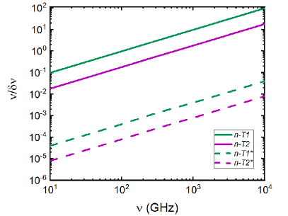
Since the minimum detectable single-photon energy depends on , our nano-TESs show different values of . In particular, we have 100 GHz ( 0.4 meV) and 540 GHz ( 2 meV) for n-T1 and n-T2, respectively. Accordingly, the resolving power (), which indicates the sensitivity in detecting radiation of a specific energy, achieves values larger than for GHz for n-T1, as shown in Fig. 6. We note that the sensitivity of the devices could be further improved by increasing the sharpness of the superconducting to normal-state transition of the active region, i.e. rising the value of .
In the absence of AM, the electron heat capacitance increases of about 7 orders of magnitude due the volume increase. Therefore, the frequency resolution downgrades of more than 3 orders of magnitude (see Tab. 1), and the devices could operate only above 300 THz.
VII Multiplexing circuits for detector arrays
Astronomy and astrophysical experiments require telescopes equipped with arrays of hundreds or thousands detectors. Therefore, efficient multiplexing schemes are fundamental to decrease the wiring, lower the related noise, and reduce the mechanical and thermal loads. Several multiplexing architectures differing for the output signals are used: time division multiplexing TDM, code division multiplexing CDM, frequency division multiplexing FDM and microwave resonator MR based read-out Ullom .
For the frequency operation range and the target applications of our nano-TESs, FDM and MR represent the optimal strategies to create multipixel detectors. Thus, we will estimate the circuit parameters to build arrays of our nano-TESs.
VII.1 Frequency Division Multiplexing
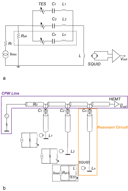
The FDM circuit is schematically shown in Fig 7-a Lanting ; Vaccaro . Each unit cell operates at its own frequency [] defined by the RCL circuit and adequately separated from the others to avoid cross talk. The signal bandwidth of each pixel is larger than the relaxation effective time-scale of the nano-TES after the photon absorption () suppressing all noise signals outside the band. In order to have a signal bandwidth [] constant for each pixel of the array, the same inductance is usually set for every channel. For example, considering the values of n-T2 we propose a bandwidth of kHz, an inductance of H and a capacitance range between pF and pF to have pixels for an array. Therefore, each pixel has a resonance frequency between MHz and MHz, and it is spaced of kHz to suppress cross-talk. The total signal is measured with a single SQUID amplifier of time constant shorter than the effective pulse recovery time to follow the current variation in the nano-TES (). Its bandwidth BW of 20 MHz is consistent with state-of-the-art SQUID amplifiers Muck ; Huber . Custom LC lithographed boards with multiplexing factors can be fabricated to this end. The generation of tones and subsequent demodulation can be handled by electronic boards equipped with FPGAs suitably designed Dobbs .
VII.2 Microwave resonator multiplexing
The MR multiplexing exploits a SQUID amplifier connecting the sensing elements of each pixel to a different RLC resonant circuit (see Fig. 7-b). This configuration maximizes the dynamic range per pixel and removes the limit on the pixel number, but the system is more bulky.
Photon absorption shifts the resonance of the related circuit which is connected in parallel and excited simultaneously to all the others. Then, the transmitted signals are summed into a low noise amplifier, such as the high electron mobility transistor (HEMT) placed at a higher temperature.
The bandwidth of n-T2 is MHz. Considering a SQUID amplifier with bandwidth MHz, we can choose resonant circuits with bandwidth MHz separated by MHz in frequency range going from MHz to GHz.
To this end, each line could implement systems with resistance of , fixed inductance of 0.2 F and capacitance values between pF and pF. Therefore, the MR would allow to build arrays of nano-TESs with high dynamic range, low power dissipation and giving the possibility to select a larger bandwidth.
VIII Summary and conclusions
We have presented an extra-sensitive and optimized miniaturized structure, which can be used as a nanoscale transition edge sensor (nano-TES). The ultra-low volume of the active region and the exploitation of heat barriers, the so-called Andreev mirrors, ensure the optimal thermal efficiency of the devices. In addition, the engineering of the working temperature thanks to the superconducting inverse proximity effect allows full control of the nano-TES performance. To extract all the device parameters and determine the performance both in the bolometer and calorimeter operation, we performed a complete series of experiments. On the one hand, by characterizing electrically the nano-TES we measured the critical current and the critical temperature of the active region. On the other hand, we fabricated and characterized a secondary device equipped with superconducting tunnel probes extracting the spectral and thermal properties of .
Starting from the experimental data, we calculated the performance of our device when operated as a nano-TES by employing widespread and well known equations. The nano-TES is predicted to reach a total noise equivalent power of W/, limited exclusively by the thermal fluctuations, when operated as bolometer. In single-photon detection, our device shows a best frequency resolution of GHz, thus having the potential to operate in THz and sub-THz regime with a relaxation time of 10 ns.
With its simple design, the nano-TES could be implemented in widespread multiplexing circuits (FDM and MW Resonators) for detector arrays in multipixel gigahertz cameras Ullom . As a consequence, the nano-TES could become an asset as bolometer and calorimeter for astronomy and astrophysics research, detecting cosmic microwave background Sironi and atomic vibration in galaxy cluster Villaescusa-Navarro , and be the key for searching axions (Redondo, ; Ringwald, ; Spagnolo, ), one of the principal candidates of dark matter. Moreover, it could find application for medical imaging Sun , industrial quality controls Ellrich and security Rogalski in THz band.
acknowledgements
We acknowledge A. Tartari, and G. Lamanna for fruitful discussions. The authors acknowledge the European Union’s Horizon 2020 research and innovation programme under the grant No. 777222 ATTRACT (Project T-CONVERSE) and under grant agreement No. 800923-SUPERTED. The authors acknowledge CSN V of INFN under the technology innovation grant SIMP. The work of F.P. was partially supported by the Tuscany Government (Grant No. POR FSE 2014-2020) through the INFN-RT2 172800 project. The work of V.B. is partially funded by the European Union (Grant No. 777222 ATTRACT) through the T-CONVERSE project. G.S. acknowledges the ASI grant 2016-24-H.0.
Conflict of interest
The authors declare that they have no conflict of interest.
Data availability
The data that support the findings of this study are available from the corresponding author upon reasonable request.
References
- (1) G. Sironi, The frequency spectrum of the Cosmic Microwave Background, New Astron. Rev. 43, 243-249 (1999).
- (2) F. Villaescusa-Navarro, S. Planelles, S. Borgani, M. Viel, E. Rasia, G. Murante, K. Dolag, L. K. Steinborn, V. Biffi, A. M. Beck, and C. Ragone-Figueroa, Neutral hydrogen in galaxy clusters: impact of AGN feedback and implications for intensity mapping, Monthly Notices of the Royal Astronomical Society 456, 4 pp 3553–3570 (2016).
- (3) I. G. Irastorza, and J. Redondo, New experimental approaches in the search for axion-like particles, Prog. Part. Nucl. Phys. 102, 89 (2018).
- (4) U. Seljak, and M. Zaldarriaga, Signature of Gravity Waves in the Polarization of the Microwave Background, Phys. Rev. Lett. 78, 2054 (1997).
- (5) M. Kamionkowski, and E. D. Kovetz, The Quest for B Modes from Inflationary Gravitational Waves, Annual Rev. Astron. and Astroph. 54, 227–269 (2016).
- (6) L. Armus, V. Charmandaris, and B.T. Soifer, Observations of luminous infrared galaxies with the Spitzer Space Telescope. Nat Astron 4, 467–477 (2020).
- (7) A. Ringwald, Exploring the role of axions and other WISPs in the dark universe, Phys. Dark Univ. 1, pp.116-135 (2012).
- (8) L. M. Capparelli, G. Cavoto, J. Ferretti, F. Giazotto, A. D. Polosa, and P. Spagnolo, Axion-like particle searches with sub-THz photons, Phys. Dark Univ. 12, 37-44 (2016).
- (9) M. Arik et al., New solar axion search using the CERN Axion Solar Telescope with 4He filling, Phys. Rev. D 92, 021101 (2015).
- (10) E. Armengaud et al., Conceptual Design of the International Axion Observatory (IAXO), JINST 9, T05002 (2014).
- (11) K. D. Irwin, Seeing with Superconductors, Sci. Am. 295, 86-94 (2006).
- (12) K. D. Irwin, An application of electrothermal feedback for high resolution cryogenic particle detection, Applied Physics Letters 66, (1995).
- (13) B. S. Karasik, R. Cantor, Demonstration of high optical sensitivity in far-infrared hot-electron bolometer, Appl. Phys. Lett. 98, 193503 (2011).
- (14) A. Monfardini, et. al. Lumped element kinetic inductance detectors for space applications, in Proc. SPIE 9914, Millimeter, Submillimeter, and Far-Infrared Detectors and Instrumentation for Astronomy VIII, 99140N (2016).
- (15) P. Khosropanah, et al. Low noise transition edge sensor (TES) for the SAFARI Instrument on SPICA. in Proc. SPIE 7741, Millimeter, Submillimeter, and Far-Infrared Detectors and Instrumentation for Astronomy V, 77410L (2010).
- (16) P. de Visser, J. Baselmans, J. Bueno, et al. Fluctuations in the electron system of a superconductor exposed to a photon flux, Nat Commun 5, 3130 (2014).
- (17) J. Wei, D. Olaya, B. S. Karasik, S. V. Pereverzev, A. V. Sergeev, and M. E. Gershenson, Ultrasensitive hot-electron nanobolometers for terahertz astrophysics, Nat Nanotech. 3, 496–500 (2008).
- (18) R. Kokkoniemi, et al., Nanobolometer with ultralow noise equivalent power, Commun Phys 2, 124 (2019).
- (19) L. S. Kuzmin, et al., Photon-noise-limited cold-electron bolometer based on strong electron self-cooling for high-performance cosmology missions, Commun Phys 2, 104 (2019).
- (20) P. Virtanen, A. Ronzani, and F. Giazotto, Josephson Photodetectors via Temperature-to-Phase Conversion, Phys. Rev. Applied 9, 054027 (2018).
- (21) F. Paolucci, N. Ligato, V. Buccheri, G. Germanese, P. Virtanen, and F. Giazotto, Hypersensitive tunable Josephson escape sensor for gigahertz astronomy, Phys. Rev. Applied 14, 034055 (2020).
- (22) D. Alesini et al., Status of the SIMP Project: Toward the Single Microwave Photon Detection, J. Low Temp. Phys. 199, 348–354 (2020).
- (23) T. Bergmann, Energy resolving power of transition edge x-ray microcalorimeters, Phd Dissertation, University of Utrecht (2004).
- (24) A. F. Andreev, The Thermal Conductivity of the Intermediate State in Superconductors. JETP 66, 1228-1231 (1964).
- (25) Q. Sun , Y. He, K. Liu, S. Fan, E. P. J. Parrott, and E. Pickwell-MacPherson, Recent Advances in Terahertz Technology for Biomedical Applications, Quant. Imaging Med. Surg. 7, 345-355 (2017).
- (26) F. Ellrich, M. Bauer, N. Schreiner, et al., Terahertz Quality Inspection for Automotive and Aviation Industries, J. Infrared Milli. Terahz. Waves 41, 470–489 (2020)
- (27) A. Rogalski, F. Sizov, Terahertz detectors and focal plane arrays, Opto-Electronics Review 19, (2011).
- (28) M. Tinkham, Introduction to Superconductivity, McGraw Hill (1996).
- (29) F. Giazotto, T. T. Heikkila, A. Luukanen, A. M. Savin, and J. P. Pekola, Opportunities for mesoscopics in thermometry and refrigeration: Physics and applications. Rev. Mod. Phys. 78, 217-274 (2006).
- (30) H. Courtois, M. Meschke, J. T. Peltonen, and J. P. Pekola, Origin of Hysteresis in a Proximity Josephson Junction, Phys. Rev. Lett. 101, 067002 (2008).
- (31) J. F. Cochran and D. E. Mapother, Superconducting Transition in Aluminum, Phys Rev. 111, 132 (1958).
- (32) P. G. De Gennes, Boundary Effects in Superconductors, Rev. Mod. Phys. 36, 225 (1964).
- (33) V. G. Kogan, Coherence length of a normal metal in a proximity system, Phys. Rev. B 26, 88 (1982).
- (34) R. Meservey and P. M. Tedrow, Properties of Very Thin Aluminum Films, Journal of Applied Physics 42, 51 (1971).
- (35) F. C. Wellstood, C. Urbina, and J. Clarke, Phys. Rev. B 49, 5942 (1994).
- (36) R. Bosisio, P. Solinas, A. Braggio, and F. Giazotto, Photonic heat conduction in Josephson-coupled Bardeen-Cooper-Schrieffer superconductors, Phys. Rev. B 93, 144512 (2016).
- (37) T. T. Heikkilä, M. Hatamib, and G. E. W. Bauerb, Electron–electron interaction induced spin thermalization in quasi-low-dimensional spin valves, Solid State Commun. 150, 475 (2010).
- (38) Irwin K. D. and Hilton G.C., Cryogenic Particle Detection, Springer Topics Appl. Phys. 99, (2005).
- (39) K. D. Irwin, Phonon-mediated particle detection using superconducting tungsten transition-edge sensors, Ph.D. Thesis, Stanford University (1995).
- (40) J. C. Mather, Bolometer noise: non equilibrium theory, Appl. Opt. 21, 1125-1129 (1982).
- (41) S. Lee, J. M. Gildemeister, W. Holmes, A. T. Lee, and P. L. Richards, Voltage-biased superconducting transition-edge bolometer with strong electrothermal feedback operated at 370 mK, Appl. Opt. 37, 3391-3397 (1998).
- (42) K. Morgan, Hot science with cool sensors, Phys. Today 71, 28-34 (2018).
- (43) J. N. Ullom, D. A. Bennet, Review of superconducting transition-edge sensors for x-ray and gamma-ray spectroscopy, Supercond. Sci. Technol 28, (2015).
- (44) T. M. Lanting, H. Cho, J. Clarke, M. Dobbs, A. T. Lee, P. L. Richards, H. Spieler, A. Smith, Frequency-domain multiplexing for large-scale bolometer arrays, Proceedings, 4855, Millimeter and Submillimeter Detectors for Astronomy, (2003).
- (45) A. Tartari, A. M. Baldini, F. Cei, L. Galli, M. Grassi, D. Nicolò, M. Piendibene, F. Spinella, D. Vaccaro, and G. Signorelli , Development and Testing of the FDM Read-Out of the TES Arrays Aboard the LSPE/SWIPE Balloon-Borne Experiment, J Low Temp Phys 199, 212–218 (2020)
- (46) J. Yoon, J. Clarke, J. M. Gildemeister, A. T. Lee, M. J. Myers, P. L. Richards, and J. T. Skidmore, Single superconducting quantum interference device multiplexer for arrays of low-temperature sensors, Applied Physics Letters 78, 371 (2001).
- (47) M Mück, M-O. André, and J. Clarke, Radio-frequency amplifier based on a niobium dc superconducting quantum interference device with microstrip input coupling, Appl. Phys. Lett. 72, 2885 (1998).
- (48) M. E. Huber, et. al, DC SQUID series array amplifiers with 120 MHz bandwidth, IEEE Trans. Appl. Supercond 1, 1251-1256 (2001).
- (49) A. M. Dobbs, et al. Frequency Multiplexed SQUID Readout of Large Bolometer Arrays for Cosmic Microwave Background Measurements, Rev. Sci. Instrum. 83, 073113 (2012).