Embracing the Unreliability of Memory Devices
for Neuromorphic Computing
††thanks: This work was supported by the ERC Grant NANOINFER (715872) and the ANR grant NEURONIC (ANR-18-CE24-0009).
Abstract
The emergence of resistive non-volatile memories opens the way to highly energy-efficient computation near- or in-memory. However, this type of computation is not compatible with conventional ECC, and has to deal with device unreliability. Inspired by the architecture of animal brains, we present a manufactured differential hybrid CMOS/RRAM memory architecture suitable for neural network implementation that functions without formal ECC. We also show that using low-energy but error-prone programming conditions only slightly reduces network accuracy.
I Introduction
Emerging nonvolatile memory technologies such as resistive, phase change and spin torque magnetoresistive memories offer considerable opportunities to advance microelectronics, as these memories are faster than flash memories, while being compact and compatible with the integration in the backend-of-line of modern CMOS processes [1, 2]. However, although these technologies are usually more reliable than flash memories, they remain considerably less reliable than volatile charge-based random access memories. Strategies for reducing errors due to device variation and limited endurance involve costly materials and technology developments [3], energy-consuming special programming strategies [4], and quite universally, the reliance on advanced multiple error correcting codes (ECC) [1, 5], requiring large area and energy hungry decoding circuitry [6].
The existence of errors in emerging memories is also a severe limitation for the development of in or near-memory computing schemes, which aim at achieving highly energy efficient computation by eliminating the von Neumann bottleneck [7, 1]. In or near-memory computing schemes are indeed hardly compatible with ECC, as computation is performed with multiple row selection or in the sensing circuit [8, 9]. These constrains are in sharp contrast with animal brains, which function with vastly unreliable, redundant, memory devices (synapses) without using formal error correction [10, 11].
In this work, we show through an example that in computing architectures inspired by brains (neuromorphic architectures), memory device variability can to a large extent be ignored, and even embraced, and that this attitude can provide important benefits. We first present a differential memory architecture optimized for the ECC-less in-memory implementation of biarized neural networks. We show based on experimental measurements on a fabricated CMOS/RRAM hybrid chip and on network simulations that this architecture can mostly ignore device variation, and investigate the benefits of accepting errors. Based on a modeling study, we show that the same methodology could be transferred to MRAM.
II An In-Memory Computing Memory Block That Functions With Error-Prone Devices
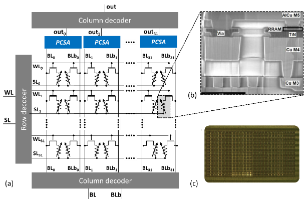
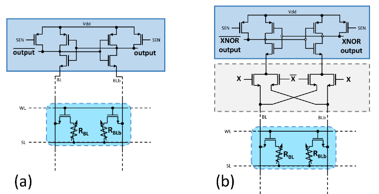
In this work, we propose the use of a memory architecture where each bit is stored in a two-transistor/two-resistor (2T2R) cell. We implemented a kilobit version (2,048 devices) of this architecture in a 130 nm CMOS technology, with hafnium oxide-based RRAM fully embedded in the backend-of-line (Fig. 1). This test chip was initially introduced in [8, 9]. Bits are stored in a differential fashion between the two devices to reduce errors. Doing so, during the read phase, a high resistive state (HRS) is always compared to a low resistive state (LRS), doubling the memory read window with regards to the conventional comparison to a reference value between HRS and LRS, as is used in one-transistor/one-resistor (1T1R) architectures [8]. This differential read scheme is operated by on-chip precharge sense amplifiers (PCSA), whose circuit is presented in Fig. 2(a). These sense amplifiers can also be augmented to directly perform logic operations during read operations [12]. An example where a PCSA has been augmented to perform exclusive NOR (XNOR) operation is shown in Fig. 2(b). Such in-memory computing augmentations, while approaching logic and memory, make our system incompatible with conventional ECC scheme.
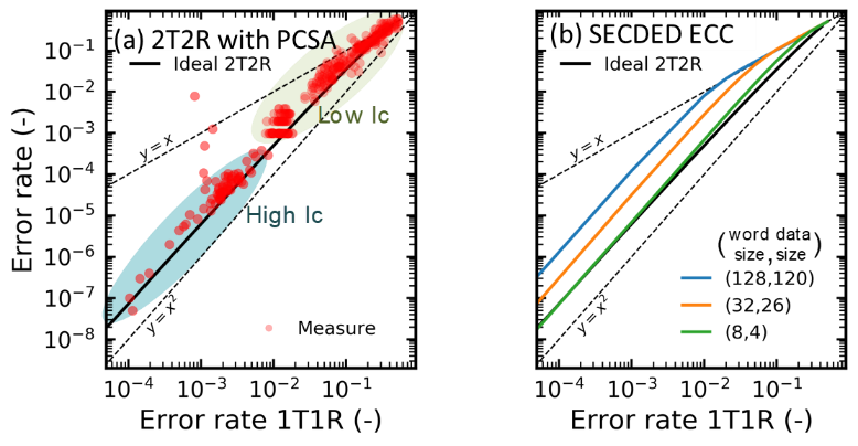
Extensive experimental measurements on our test chip showed that the 2T2R strategy indeed reduces bit errors when compared to the classical 1T1R approach. RRAM devices error rate is directly linked to the current used during the programming operations, offering a knob of error rate tuning depending on the application requirements. Fig. 3(a) compiles statistical measurements on the fabricated test chip, taken with diverse programming currents, allowing evaluating the bit error rates (BER) benefits of the 2T2R approach in different conditions. It is apparent in this Figure that the 2T2R strategy always reduces the amount of bit errors, with the highest benefits seen at lower BERs. The detailed methodology for obtaining Fig. 3(a) is presented in [9].
Quite interestingly the error reduction benefits of the 2T2R approach are similar to the one of a Single Error Correcting Double Error Detecting ECC (SECDED, or extended Hamming), but without the high peripheral circuit overhead required by this ECC [6], and associated read performance degradation (Fig. 3(b)). Moreover, this result is obtained considering the same memory capacity (2T2R without ECC versus 1T1R plus extra bit for correction code storage).
III Benefits at the Network Level

Binarized Neural Networks (BNNs) [14], or the highly similar XNOR-NETs [15], are a recently proposed type of neural network, where synaptic weights and neuron states can take only binary values (meaning and ) during inference (whereas these parameters assume real values in conventional neural networks). Therefore, the equation for the activation of a neuron in a conventional neural network
| (1) |
(where are inputs of the neuron, the synaptic weights and its nonlinear activation function) simplifies into
| (2) |
is an integer function that counts the number ones. is the sign function, and is the threshold of the neuron, obtained during training by the use of the batch-normalization technique [16].
BNNs can achieve surprisingly high accuracy in vision [15, 17] or signal-processing [18] tasks. BNNs have highly reduced memory requirements with regards to real neural networks, and have the added benefit of not requiring any multiplication, as this operation is replaced by XNOR logic operations. These advantages make BNNs outstanding candidates for in-memory computing [19, 20, 21, 22, 23, 24, 25, 26].
The architecture of Fig. 1 is particularly adapted for the ECC-less implementation of such neural networks. For example, Fig. 4 shows a full system using memory circuits of Fig. 1 to implement a BNN. The architecture uses the sense amplifier of Fig. 2(b) [12] to implement XNOR operations directly in each memory circuit during the read phase, whereas the operation, as well as neuron activation are performed on foot of array columns using fully digital circuits. Refs. [9, 27] describe this architecture in detail, as well as some its variations, and show that this architecture features outstanding energy-efficiency properties.
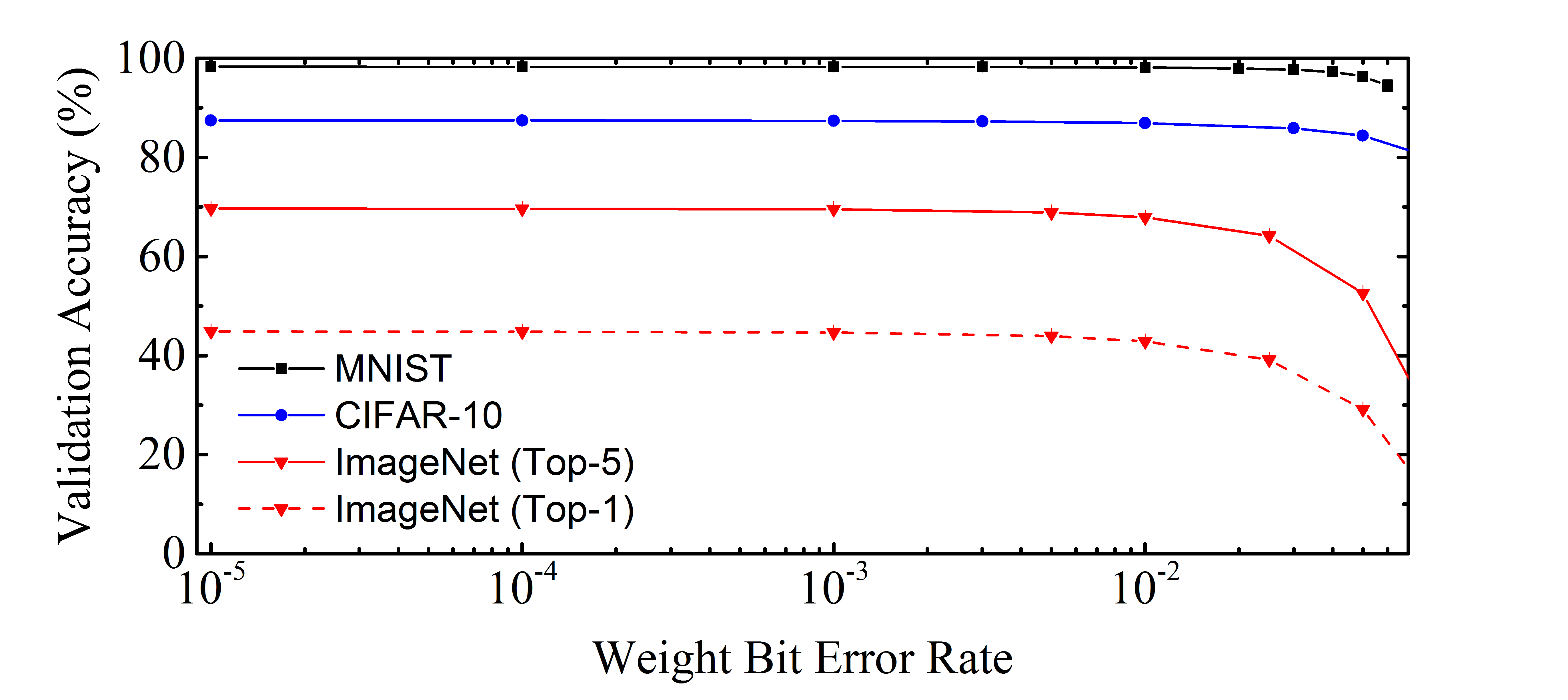
We now evaluate the impact of errors in memories in this architecture. Fig. 5 shows simulations of the architecture programmed to perform several tasks: the classic MNIST handwritten digit recognition task [28], the CIFAR-10 image classification task [29], and the challenging ImageNet classification task, which consists in classifying high-resolution images into 1,000 classes [30]. The detailed architecture of the BNNs used on these three tasks in presented in [9]. All these tasks were simulated with various bit error rates on the memory devices. Quite astonishingly, we see on all these three tasks that bit error rate as high as can be tolerated with little consequence on the accuracy of the implemented neural network. This highlights that when implementing BNNs, memory perfection is far from being required. Some dedicated training strategies could enhance this error tolerance even further [31].
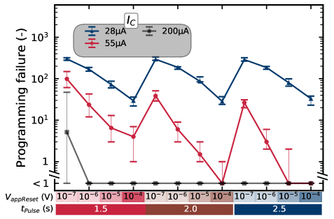
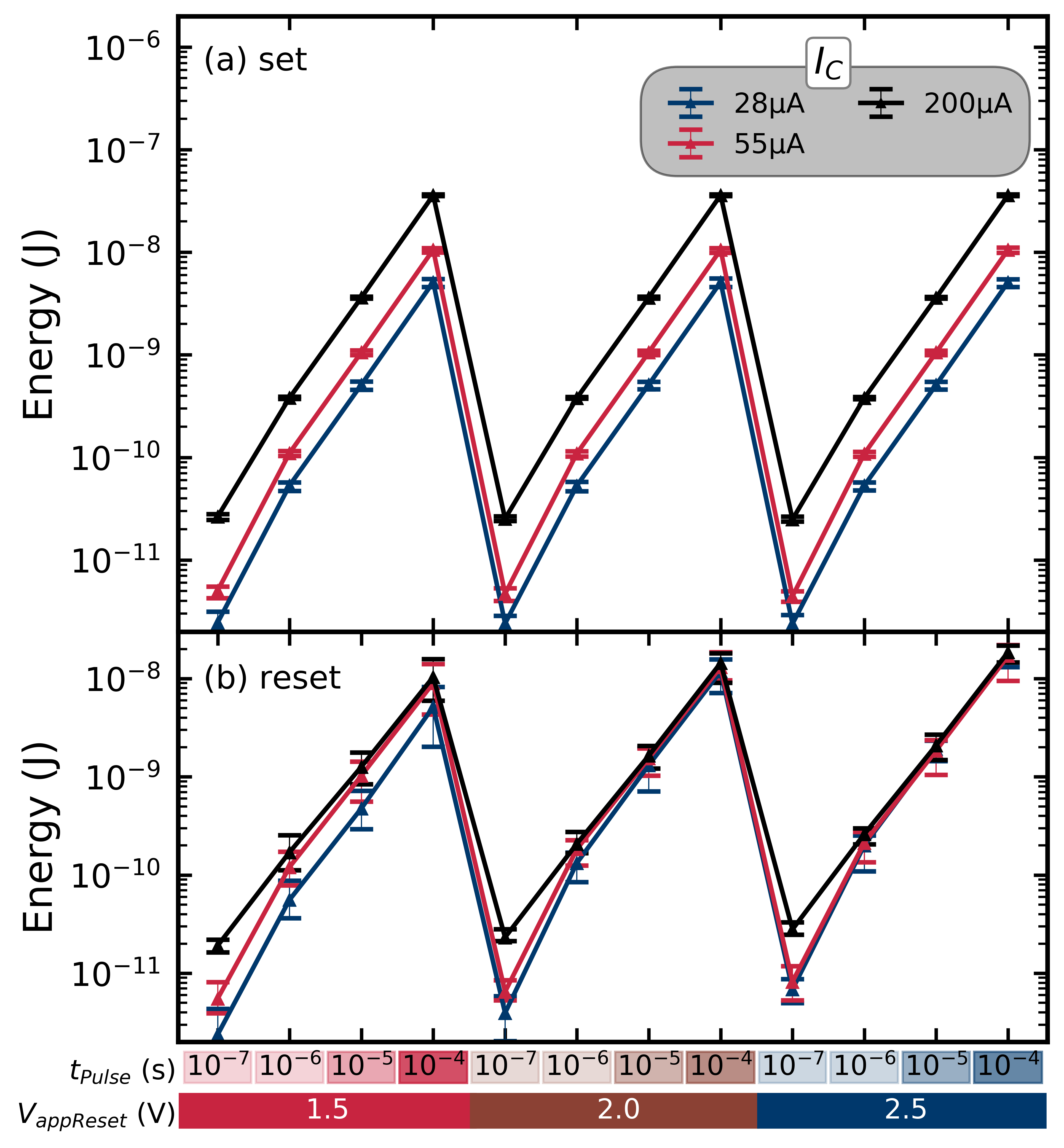
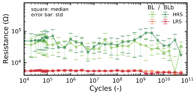
The combination of the fact that the 2T2R approach allows reducing the amount of bit errors, and that the BNN application features inherent tolerance to bit errors has important consequences in practice. It allows us to use RRAM devices in regimes where they are extremely unreliable. This can provide important energy savings: we can use devices with very weak programming conditions (low current and voltages, short programming time), where they feature high amounts of bit errors. Figs. 6 and 7 show statistical measurements of our test chip in various conditions, and highlight the energy benefits of accepting more errors. Finally, operating devices in high BER regimes allows using conditions where they feature outstanding endurance. Fig. 8 for example shows endurance measurements of two devices programmed with low RESET voltages (). An endurance of more than cycles is seen, which is particularly high for such technology. This type of high cyclability opens the way to the possibility of training neural networks on chip, as seen in the results reported in [32]. A more detailed analysis of the energy benefits (which can reach a factor ten) of embracing bit errors in RRAM-based BNNs, and of the associated endurance benefits, is presented in [9].
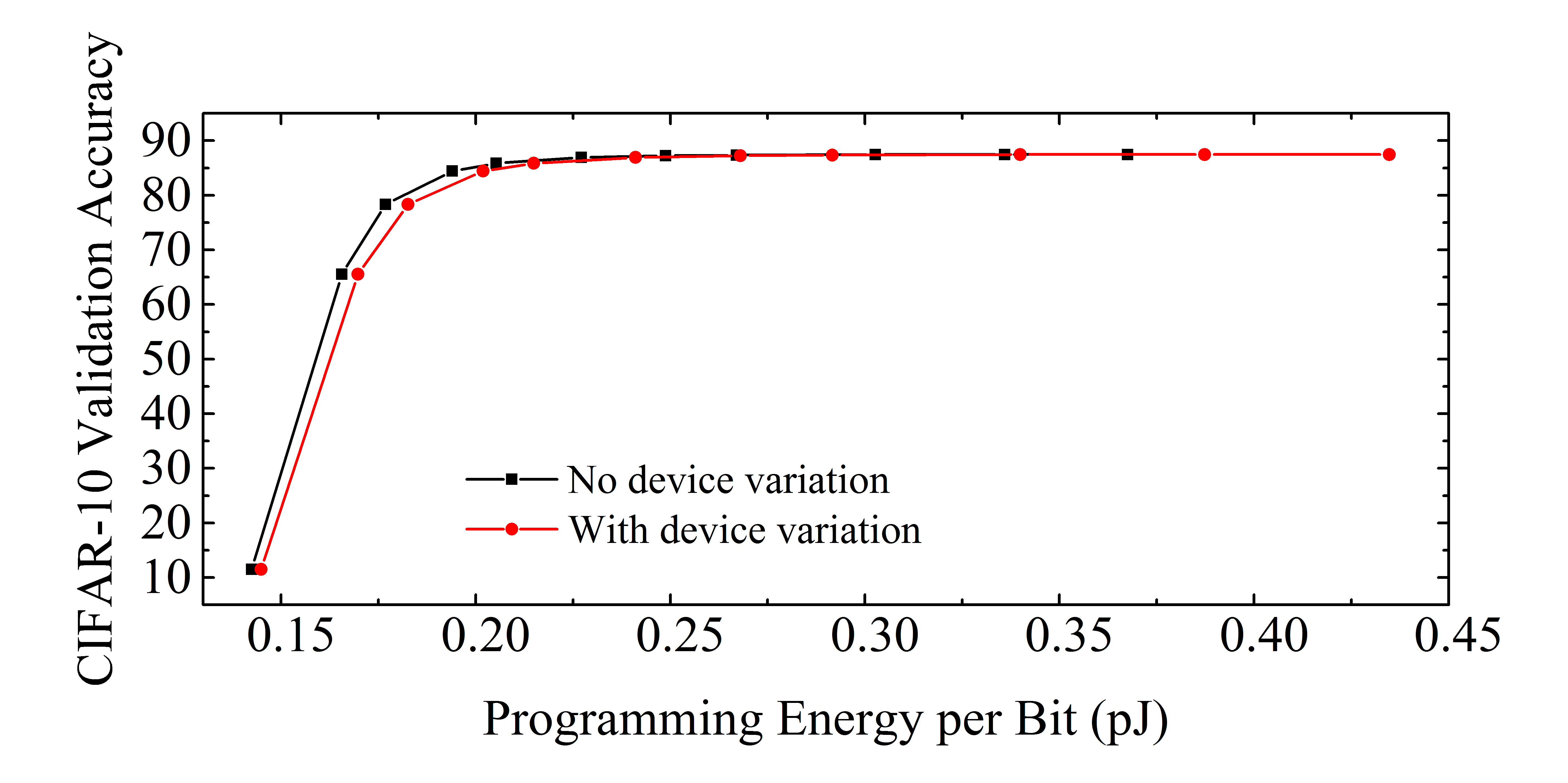
The strategy reported in this work is not limited to RRAM, and can be applied to other types of memories. Fig. 9 shows, based on neural network simulation, the energy that could be saved by varying the programming time of 28 nm Spin Torque Magnetoresistive RAM (ST-MRAM) using the same approach as the one presented here. We see that high energy savings can be achieved. The methodology and model for obtaining these results are presented in [13].
IV Conclusion
Digital computing usually assumes and requires perfection in the memory bits, and this accuracy comes at important costs in terms of area and energy consumption. In contrast, neuromorphic circuits, including fundamentally digital ones such as binarized neural networks can get away with imperfect memory cells. In this work, we use a differential approach to reduce errors and to be compatible with in or near-memory computing. This differential coding, in combination with the inherent tolerance of neural network, shows that it is possible on one side to embrace memories as “non ideal” without noticeable impact on neural network accuracy, and on the other side to get important benefits in terms of tuning of operating conditions (endurance, energy), opening the way to on-chip learning.
References
- [1] D. Ielmini and H.-S. P. Wong, “In-memory computing with resistive switching devices,” Nature Electronics, vol. 1, no. 6, p. 333, 2018.
- [2] S. Yu, “Neuro-inspired computing with emerging nonvolatile memorys,” Proc. IEEE, vol. 106, no. 2, pp. 260–285, 2018.
- [3] F. M. Bayat, M. Prezioso, B. Chakrabarti, H. Nili, I. Kataeva, and D. Strukov, “Implementation of multilayer perceptron network with highly uniform passive memristive crossbar circuits,” Nature communications, vol. 9, no. 1, pp. 1–7, 2018.
- [4] M.-F. Chang, J.-J. Wu, T.-F. Chien, Y.-C. Liu, T.-C. Yang, W.-C. Shen, Y.-C. King, C.-J. Lin, K.-F. Lin, Y.-D. Chih et al., “19.4 embedded 1mb reram in 28nm cmos with 0.27-to-1v read using swing-sample-and-couple sense amplifier and self-boost-write-termination scheme,” in Proc. ISSCC. IEEE, 2014, pp. 332–333.
- [5] O. Golonzka, J.-G. Alzate, U. Arslan, M. Bohr, P. Bai, J. Brockman, B. Buford, C. Connor, N. Das, B. Doyle et al., “Mram as embedded non-volatile memory solution for 22ffl finfet technology,” in 2018 IEEE International Electron Devices Meeting (IEDM). IEEE, 2018, pp. 18–1.
- [6] S. Gregori, A. Cabrini, O. Khouri, and G. Torelli, “On-chip error correcting techniques for new-generation flash memories,” Proc. IEEE, vol. 91, no. 4, pp. 602–616, 2003.
- [7] Editorial, “Big data needs a hardware revolution,” Nature, vol. 554, no. 7691, p. 145, Feb. 2018.
- [8] M. Bocquet, T. Hirztlin, J.-O. Klein, E. Nowak, E. Vianello, J.-M. Portal, and D. Querlioz, “In-memory and error-immune differential rram implementation of binarized deep neural networks,” in IEDM Tech. Dig. IEEE, 2018, p. 20.6.1.
- [9] T. Hirtzlin, M. Bocquet, B. Penkovsky, J.-O. Klein, E. Nowak, E. Vianello, J.-M. Portal, and D. Querlioz, “Digital biologically plausible implementation of binarized neural networks with differential hafnium oxide resistive memory arrays,” Frontiers in Neuroscience, vol. 13, p. 1383, 2020.
- [10] A. A. Faisal, L. P. Selen, and D. M. Wolpert, “Noise in the nervous system,” Nature reviews neuroscience, vol. 9, no. 4, p. 292, 2008.
- [11] K. Klemm and S. Bornholdt, “Topology of biological networks and reliability of information processing,” Proceedings of the National Academy of Sciences, vol. 102, no. 51, pp. 18 414–18 419, 2005.
- [12] W. Zhao et al., “Synchronous non-volatile logic gate design based on resistive switching memories,” IEEE Transactions on Circuits and Systems I: Regular Papers, vol. 61, no. 2, pp. 443–454, 2014.
- [13] T. Hirtzlin, B. Penkovsky, J.-O. Klein, N. Locatelli, A. F. Vincent, M. Bocquet, J.-M. Portal, and D. Querlioz, “Implementing binarized neural networks with magnetoresistive ram without error correction,” arXiv preprint arXiv:1908.04085, 2019.
- [14] M. Courbariaux, I. Hubara, D. Soudry, R. El-Yaniv, and Y. Bengio, “Binarized neural networks: Training deep neural networks with weights and activations constrained to+ 1 or-1,” arXiv preprint arXiv:1602.02830, 2016.
- [15] M. Rastegari, V. Ordonez, J. Redmon, and A. Farhadi, “Xnor-net: Imagenet classification using binary convolutional neural networks,” in Proc. ECCV. Springer, 2016, pp. 525–542.
- [16] S. Ioffe and C. Szegedy, “Batch normalization: Accelerating deep network training by reducing internal covariate shift,” arXiv preprint arXiv:1502.03167, 2015.
- [17] X. Lin, C. Zhao, and W. Pan, “Towards accurate binary convolutional neural network,” in Advances in Neural Information Processing Systems, 2017, pp. 345–353.
- [18] B. Penkovsky, M. Bocquet, T. Hirtzlin, J.-O. Klein, E. Nowak, E. Vianello, J.-M. Portal, and D. Querlioz, “In-memory resistive ram implementation of binarized neural networks for medical applications,” in Design, Automation and Test in Europe Conference (DATE), 2020.
- [19] S. Yu, Z. Li, P.-Y. Chen, H. Wu, B. Gao, D. Wang, W. Wu, and H. Qian, “Binary neural network with 16 mb rram macro chip for classification and online training,” in IEDM Tech. Dig. IEEE, 2016, pp. 16–2.
- [20] E. Giacomin, T. Greenberg-Toledo, S. Kvatinsky, and P.-E. Gaillardon, “A robust digital rram-based convolutional block for low-power image processing and learning applications,” IEEE Transactions on Circuits and Systems I: Regular Papers, vol. 66, no. 2, pp. 643–654, 2019.
- [21] X. Sun, X. Peng, P.-Y. Chen, R. Liu, J.-s. Seo, and S. Yu, “Fully parallel rram synaptic array for implementing binary neural network with (+ 1,- 1) weights and (+ 1, 0) neurons,” in Proc. ASP-DAC. IEEE Press, 2018, pp. 574–579.
- [22] X. Sun, S. Yin, X. Peng, R. Liu, J.-s. Seo, and S. Yu, “Xnor-rram: A scalable and parallel resistive synaptic architecture for binary neural networks,” algorithms, vol. 2, p. 3, 2018.
- [23] T. Tang, L. Xia, B. Li, Y. Wang, and H. Yang, “Binary convolutional neural network on rram,” in Proc. ASP-DAC. IEEE, 2017, pp. 782–787.
- [24] Z. Zhou, P. Huang, Y. Xiang, W. Shen, Y. Zhao, Y. Feng, B. Gao, H. Wu, H. Qian, L. Liu et al., “A new hardware implementation approach of bnns based on nonlinear 2t2r synaptic cell,” in 2018 IEEE International Electron Devices Meeting (IEDM). IEEE, 2018, pp. 20–7.
- [25] D. Bankman, L. Yang, B. Moons, M. Verhelst, and B. Murmann, “An always-on 3.8j/86% cifar-10 mixed-signal binary cnn processor with all memory on chip in 28-nm cmos,” IEEE Journal of Solid-State Circuits, vol. 54, no. 1, pp. 158–172, 2018.
- [26] C.-C. Chang, M.-H. Wu, J.-W. Lin, C.-H. Li, V. Parmar, H.-Y. Lee, J.-H. Wei, S.-S. Sheu, M. Suri, T.-S. Chang et al., “Nv-bnn: An accurate deep convolutional neural network based on binary stt-mram for adaptive ai edge,” in 2019 56th ACM/IEEE Design Automation Conference (DAC). IEEE, 2019, pp. 1–6.
- [27] T. Hirtzlin, B. Penkovsky, M. Bocquet, J.-O. Klein, J.-M. Portal, and D. Querlioz, “Stochastic computing for hardware implementation of binarized neural networks,” IEEE Access, vol. 7, pp. 76 394–76 403, 2019.
- [28] Y. LeCun, L. Bottou, Y. Bengio, and P. Haffner, “Gradient-based learning applied to document recognition,” Proc. IEEE, vol. 86, no. 11, pp. 2278–2324, 1998.
- [29] A. Krizhevsky and G. Hinton, “Learning multiple layers of features from tiny images,” Citeseer, Tech. Rep., 2009.
- [30] A. Krizhevsky, I. Sutskever, and G. E. Hinton, “Imagenet classification with deep convolutional neural networks,” in Advances in neural information processing systems, 2012, pp. 1097–1105.
- [31] T. Hirtzlin, M. Bocquet, J.-O. Klein, E. Nowak, E. Vianello, J.-M. Portal, and D. Querlioz, “Outstanding bit error tolerance of resistive ram-based binarized neural networks,” arXiv preprint arXiv:1904.03652, 2019.
- [32] T. Hirtzlin, M. Bocquet, M. Ernoult, J.-O. Klein, E. Nowak, E. Vianello, J.-M. Portal, and D. Querlioz, “Hybrid analog-digital learning with differential rram synapses,” in 2019 IEEE International Electron Devices Meeting (IEDM), 2019.