Coupling interlayer excitons to whispering gallery modes in van der Waals heterostructures
Abstract
Van der Waals heterostructures assembled from two-dimensional materials offer a promising platform to engineer structures with desired optoelectronic characteristics. Here we use waveguide-coupled disk resonators made of hexagonal boron nitride (h-BN) to demonstrate cavity-coupled emission from interlayer excitons of a heterobilayer of two monolayer transition metal dichalcogenides. We sandwich a MoSe2 – WSe2 heterobilayer between two slabs of h-BN and directly pattern the resulting stack into waveguide-coupled disk resonators. This enables us to position the active materials into regions of highest optical field intensity, thereby maximizing the mode overlap and the coupling strength. Since the interlayer exciton emission energy is lower than the optical band gaps of the individual monolayers and since the interlayer transition itself has a weak oscillator strength, the circulating light is only weakly reabsorbed, which results in an unaffected quality factor. Our devices are fully waveguide-coupled and represent a promising platform for on-chip van der Waals photonics.
Van der Waals (vdW) heterostructures made of a vertical assembly of two-dimensional (2D) materials like transition metal dichalcogenides (TMDCs) and graphene have opened up new possibilities for optoelectronic devices Bie et al. (2017); Flöry et al. (2020). Since adjacent 2D materials are held together by weak van der Waals forces, they can be stacked without need of lattice matching and can be placed on almost any substrate Geim and Grigorieva (2013); Liu et al. (2016). In their monolayer form, TMDCs exhibit a direct bandgap Splendiani et al. (2010); Mak et al. (2010), which makes them excellent candidates for optoelectronic devices as well as for integration with optical cavities for enhanced light matter interactions Wu et al. (2015); Ye et al. (2015); Reed et al. (2016); Li et al. (2017); Shang et al. (2017); Javerzac-Galy et al. (2018).
By combining two dissimilar TMDC monolayers into a heterobilayer (HBL), interlayer excitons with spatially separated electrons and holes can be formed Rivera et al. (2015). Their charge carrier dynamics Rigosi et al. (2015), electrically tunable exciton resonances Rivera et al. (2015); Jauregui et al. (2019) and the possibility of creating p-n junctions Ross et al. (2017), are providing intriguing possibilities for materials engineering. Recently, interlayer excitons were coupled to photonic crystal cavities Liu et al. (2019); Rivera et al. (2020), as well as grating cavities Paik et al. (2019), that led to the demonstration of surface emitting, optically pumped lasers at room-temperature Liu et al. (2019); Paik et al. (2019).
However, the co-integration of light emitting devices (LEDs) and lasers made of vdW heterostructures with on-chip photonic structures, such as waveguides and resonators, requires in-plane light guiding. Coupling via evanescent fields has been achieved, for example, by placing vdW materials on top of silicon-based waveguides Bie et al. (2017); Flöry et al. (2020) and ring resonators Wei et al. (2015), but the coupling strength obtainable in this manner is modest because the highest field intensity is found inside the light confining dielectric medium. Optimal mode overlap can be achieved by integrating the active layer into dielectric waveguides or resonators. For optically excited systems, this has been shown by sandwiching a monolayer WS2 into a microdisk made of Si3N4/hydrogen silsesquioxane (HSQ) Ye et al. (2015) or hexagonal boron nitride (h-BN) Ren et al. (2018). However, in both of these structures the disk was freestanding and is not easily compatible with on-chip photonics.
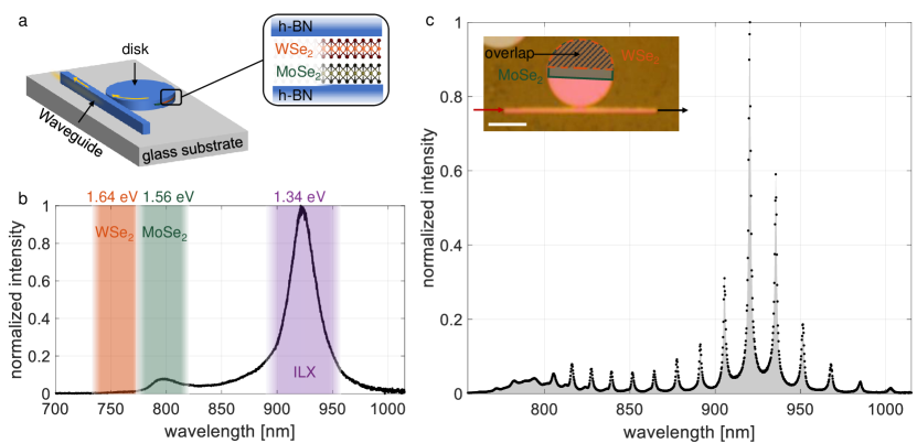
Here we present vdW heterostructures patterned into waveguide-coupled disk resonators, as illustrated in Fig. 1a. The stacking allows us to place TMDCs into regions of high field intensity. Our approach combines two important attributes: 1) an enhanced optical mode overlap and 2) waveguide coupling for on-chip integration. These are enabling factors for the development of on-chip optoelectronic devices, such as LEDs, modulators and photodetectors. For the dielectric material we chose h-BN, which has already been used to fabricate photonic structures like resonators or photonic crystals Kim et al. (2018); Ren et al. (2018); Fröch et al. (2019) and has been proposed as a confinement layer in integrated photonics Ren and Loh (2019). In addition to its favorable photonic attributes, h-BN also provides a means of encapsulation, that is, by placing TMDCs in between h-BN we prevent them from degradation Lee et al. (2015).
As shown in Fig. 1a, we integrate a HBL into an h-BN disk resonator, which can be excited by laser light propagating along a nearby waveguide. Photoluminescence (PL) associated with the interlayer exciton is coupled out by the adjacent waveguide. The unique feature of our approach is that both, the active material (TMDCs) as well as the dielectric (h-BN) are assembled into a single vdW heterostructure and subsequently patterned into the final photonic circuit (disk resonator and waveguide). This differs from previous works Bie et al. (2017); Flöry et al. (2020); Wei et al. (2015), where TMDCs were transferred on top of pre-fabricated photonic elements. As illustrated in Fig. 1b, the interlayer exciton emission energy is lower than the optical band gaps of the individual monolayers, which leads to weak reabsorption of the interlayer emission. Reabsorption is further suppressed by the weak oscillator strength of the direct interlayer exciton transition Ross et al. (2017); Förg et al. (2019). As a result, the quality (Q)-factor of the coupled mode is largely unaffected by reabsorption. Figure 1c shows the spectrum of the waveguide-coupled interlayer emission. The vdW disk has been excited from one end of the waveguide with a laser and the PL has been detected at the other end. In the following we first describe the fabrication procedure, then present the characteristics of the HBL and h-BN disks and finally discuss the results of the combined system.
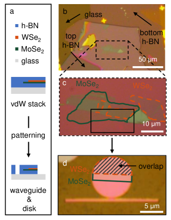
Flakes of h-BN and monolayers of WSe2 and MoSe2 were prepared by mechanical exfoliation and assembled into vdW heterstructures using a polymer-based stacking technique Wang et al. (2013); Zomer et al. (2014). The crystallographic axes of the two monolayers were rotationally aligned. Atomic force microscopy was utilized to identify h-BN flakes of the desired thicknesses. Figures 2b and c (magnified) show optical microscope images of such an h-BN – MoSe2 – WSe2 – h-BN heterostructure on a glass substrate. As illustrated in Fig. 2a, waveguides and disk resonators were fabricated from the vdW stack using electron-beam lithography and reactive ion etching with aluminum as a hard mask. Fig. 2d shows the final device. The disk resonator has a total thickness of and a design radius of . A more detailed description of the fabrication procedure can be found in the methods section in the Supporting Information (SI).
In order to determine the emission energies we performed PL measurements of the TMDC monolayers and of the HBL region using a continuous wave (cw) He-Ne laser. The PL spectra of the individual monolayers reveal direct intralayer exciton emission peaks at () and () for WSe2 and MoSe2, respectively, and are in agreement with previous works Ross et al. (2013); Rigosi et al. (2015); Karni et al. (2019); Liu et al. (2019) (details in the SI). In Fig. 1b we show the PL spectrum of the HBL, with a pronounced peak at around (). This feature is identified as the interlayer exciton emission and can be explained by the type-II band alignment of MoSe2 and WSe2 in the overlap region Rivera et al. (2015); Paik et al. (2019). In this process the absorption of a photon in a monolayer is followed by a charge transfer to the energetically favorable band of the neighboring monolayer, leading to a spatial separation of electron and hole. As a result, a strong decrease of the intralayer exciton emissions can be observed. Furthermore, for two rotationally aligned monolayers the interlayer exciton exhibits a direct band gap character Zhang et al. (2017). The strong interlayer peak in combination with the quenching of intralayer exciton emission in Fig. 1b consequently verifies the good electrical coupling and the near perfect rotational alignment of the two layers.
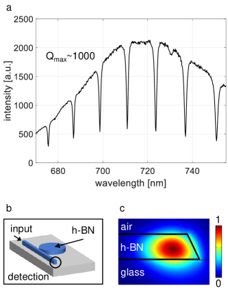
To investigate the properties of h-BN waveguide-coupled disk resonators we fabricated reference structures without integrated TMDCs. Figure 3a shows a typical transmission spectrum of a fabricated device. It was obtained by focusing a broadband supercontinuum laser on one waveguide facet and detecting the transmitted light at the other end of the waveguide. The recorded spectrum features sharp dips at wavelengths that satisfy the resonance conditions of the disk resonator. The envelope of the spectrum is defined by the excitation spectrum and the transmission characteristics of the experiment. The Q-factors of the resonances reach values of 1000. The spectral positions of the resonance peaks, the Q-factors and the free spectral range depend sensitively on the h-BN thickness and the disk radius (details in the SI). Using finite element simulations as a guide, we define the disk radius for a given stack thickness in order to optimize the resonances for the interlayer emission spectrum (details on simulations in the SI). As shown in Fig. 3c, the computed electric field distribution is highest near the rim of the disks and near the vertical center. Therefore, to optimize the coupling strength to the interlayer exciton the HBL should be sandwiched into the h-BN resonator.
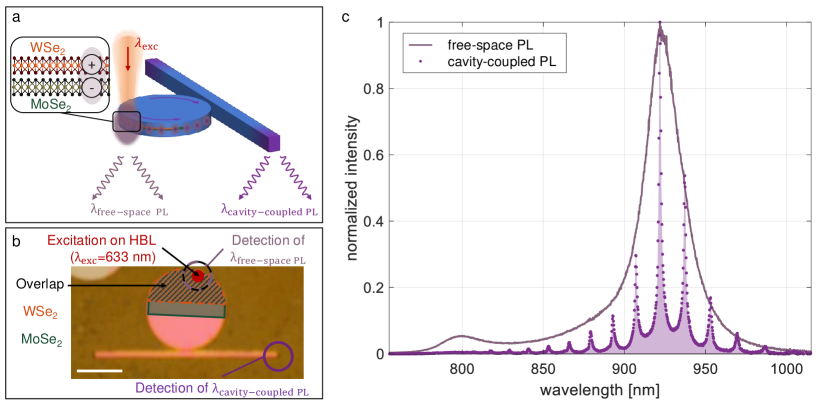
Next, we characterize an h-BN disk resonator with integrated TMDC heterobilayer. We vary the location of the excitation in order to investigate the coupling of the interlayer emission to the WGMs of the disk. As shown in the sketch and the optical microscope image in Figs. 4a and b, coupling to WGMs and interlayer excitons can be achieved by placing the excitation spot near the edge of the disk. We use the same objective for excitation and detection. The emission is detected either at the same position as the excitation spot or at the ends of the waveguide. The light coupled out at the end of the waveguide is partially refracted into the glass substrate and can be captured at high angles with the oil-immersion objective (NA=1.4) that we use. This allows us to compare the spectra of free-space PL (detected at the excitation spot on the disk) and cavity-coupled PL (detected at the waveguide end). As shown in Fig. 4c, the spectrum of the free-space PL is in agreement with the expected interlayer emission of the HBL (cf. Fig. 1b). On the other hand, the cavity-coupled spectrum, detected at the waveguide end, exhibits distinct peaks that are separated by the free-spectral range of the WGMs of the disk resonator. We emphasize that, in contrast to several other recent studies Ye et al. (2015); Reed et al. (2016); Ren et al. (2018), the waveguide-coupled spectrum features a reduced background because it is not superimposed to free-space PL.
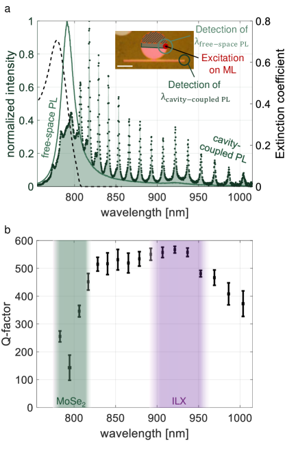
As shown in the inset of Fig. 5a, the two TMDCs forming the HBL do not overlap over the entire footprint of the disk. There are regions where only the MoSe2 monolayer can be directly excited. Figure 5a shows the corresponding spectrum of the free-space and cavity-coupled PL. The main contribution of the cavity-coupled PL comes from the intralayer exciton emission of the MoSe2 monolayer. Interestingly, however, the envelope function of the resonances does not coincide with the free-space PL, measured at the excitation spot. Instead, the highest peak intensity of the cavity-coupled PL is positioned at wavelengths longer than the free-space PL emission peak. We attribute this observation mainly to reabsorption of the emitted PL in the cavity by the MoSe2 monolayer itself, although other contributions have also been reported to be present Rosser et al. (2020) (detailed discussion in the SI). This interpretation is supported by the absorption spectrum of MoSe2, visualized by the extinction coefficient, i.e. the imaginary part of the refractive index (taken from Hsu et al. (2019)), which we include in Fig. 5a (dashed curve). Thus, the spectral overlap of the cavity-coupled PL with the extinction coefficient causes significant reabsorption for wavelengths in this spectral range. As a result, the corresponding peak intensities of the cavity-coupled PL are reduced for these wavelengths. The peaks at longer wavelengths have an additional contribution from interlayer emission from the HBL. This emission is made possible by the reabsorption of the monolayer emission in the overlap region of the two TMDCs. The effect of enhanced reabsorption in a sandwiched structure is further discussed in the Supporting Information, where two structures with integrated monolayer TMDCs are compared: 1) a sandwiched device and 2) a device with a monolayer transferred on top of the disk. The comparison shows that reabsorption in a sandwiched device is significantly stronger, due to the enhanced mode overlap.
The coupling of interlayer excitons to WGMs, profits not only from the enhanced mode overlap in the sandwiched structure, but also from low intrinsic reabsorption. The latter is due to the low oscillator strength of the interlayer transition, resulting from the spatial separation of the charge carriers Ross et al. (2017); Förg et al. (2019). The oscillator strength of the interlayer exciton in MoSe2 – WSe2 has been experimentally determined to be two orders of magnitude lower than that of the intralayer exciton Ross et al. (2017). In addition, in differential reflectance measurements, a reduced interlayer exciton absorption has also been shown, albeit at low-temperatures Förg et al. (2019). This is in agreement with our measurements shown in Fig. 4c, where the HBL has been excited. Here, the free-space PL agrees well with the envelope function of the cavity-coupled resonance peaks. To summarize, our data indicates that the intralayer emission from monolayer TMDCs is strongly reabsorbed compared to the interlayer emission. The integration of a HBL inside the disk resonator consequently has two benefits: 1) strong absorption of the excitation by intralayer excitons and 2) weak reabsorption of the interlayer emission within the cavity.
To allow for an absolute comparison of intralayer and interlayer coupling to WGMs, we now discuss waveguide-coupled excitation and read-out of the disk resonator (Fig. 1c inset). The data in Fig. 1c shows that the highest peak intensity is observed at wavelengths corresponding to the interlayer emission. In fact, the monolayer emission is strongly suppressed, in agreement with our previous conclusions. We estimate a ratio of 13 between the peak intensities of the main resonances ( and ) of interlayer and intralayer emission (details in the SI). Note that the spectrum in Fig. 1c has been corrected for the wavelength dependent transmission of our measurement setup and the CCD detection efficiency. Our waveguide-coupled experiments support our previous conclusion that intralayer emission from TMDC monolayers is largely reabsorbed.
As shown in Fig. 5b, the Q-factors of the emission peaks are wavelength dependent, which is a result of the optical properties of the incorporated TMDC HBL. The highest values are 570 and occur at wavelengths that correspond to the interlayer emission peak. In contrast, a considerably lower Q-factor is observed for wavelengths near the optical band gap of MoSe2. This provides further support for the reabsorption of monolayer emission discussed earlier. Because of the low oscillator strength of the interlayer transition the reabsorption of interlayer emission is significantly weaker, which is evidenced by the high Q-factor at wavelengths near the interlayer transition. The decrease in Q-factor at longer wavelengths () can be explained by radiation losses, which increase at higher wavelengths (see SI). Our Q-factors are currently limited by fabrication imperfections and the h-BN sidewall roughness arising from etching (see scanning electron microscope image in the SI). Nevertheless, even with integrated TMDCs and a coupled waveguide, we achieve Q-factors that are slightly higher than those reported for h-BN ring resonators Fröch et al. (2019). Our Q-factors could be increased even further by removing the substrate underneath the outer regions of the disk where the WGMs are localized Ye et al. (2015); Ren et al. (2018).
In summary, we have demonstrated the coupling of interlayer excitons from a TMDC HBL to WGMs of an h-BN disk resonator. We achieve high coupling strengths by sandwiching the HBL into the h-BN disk. The high oscillator strengths of intralayer transitions of the two monolayers lead to a high absorption efficiency. On the other hand, the low oscillator strength of the interlayer transition suppresses the reabsorption at the emission wavelength. The combination of these two effects gives rise to strong interlayer emission from our vdW disk resonators.
The presented platform would give rise to further quantitative analysis of the cavity quantum electrodynamics and experimental studies on interlayer excitons, their dynamics and emission properties, when placed at high field intensities. Considering the fact that patterning photonic structures out of h-BN and vdW heterostructures is still in its infancy, further improvements in performance with optimized fabrication techniques (e.g. optimization of the etching process) is expected. To proceed one step further towards on-chip optoelectronics, light sources need to be co-integrated with photonic structures. The recent progress in electrical control of interlayer excitons Jauregui et al. (2019), as well as the realization of light emitting devices Ross et al. (2017); Binder et al. (2019); Jauregui et al. (2019), demonstrates a wide range of possibilities for band structure engineering with HBLs. Therefore, combining our approach with electrically tunable interlayer excitons, offers a promising platform for on-chip integrated photonics based on 2D materials.
Acknowledgements.
This work has been supported by the Swiss National Science Foundation (grant 200020_192362/1). The authors thank A. Kuzmina, D. Windey, S. Papadopoulos, R. Reimann, M. Parzefall and S. Heeg for fruitful discussions. In addition the authors thank A. İmamoğlu at ETH Zürich for the usage of the stacking setup. The use of the facilities of the FIRST center for micro- and nanoscience at ETH Zürich is gratefully acknowledged. K.W. and T.T. acknowledge support from the Elemental Strategy Initiative conducted by the MEXT, Japan, Grant Number JPMXP0112101001, JSPS KAKENHI Grant Numbers JP20H00354 and the CREST(JPMJCR15F3), JST.Author contributions
L.N. and R.K. conceived the project. R.K. and P.B. fabricated the devices and performed the experiments. A.J., N.F. contributed to the experiments. S.N. and K.M. performed preliminary studies. T.T. and K.W. synthesized the h-BN crystals. R.K., P.B., N.F., A.J. and L.N. analysed the data and co-wrote the manuscript.
Supporting Information
The Supporting Information includes descriptions of: sample fabrication, methods of measurements, photoluminescence measurements, characterization of h-BN disk resonators, simulations of h-BN disk resonators, study of vertical emitter position inside h-BN disk resonator, transmission measurement of waveguide-coupled disk resonator with integrated HBL, discussion of the effect of reabsorption inside the disk resonator, determination of Q-factor, as well as comparison of the resonance peak intensities for the waveguide-coupled disk resonator with integrated heterobilayer.
References
- Bie et al. (2017) Bie, Y. Q.; Grosso, G.; Heuck, M.; Furchi, M. M.; Cao, Y.; Zheng, J.; Bunandar, D.; Navarro-Moratalla, E.; Zhou, L.; Efetov, D. K. et al. A MoTe2-based light-emitting diode and photodetector for silicon photonic integrated circuits. Nature Nanotechnology 2017, 12, 1124–1129.
- Flöry et al. (2020) Flöry, N.; Ma, P.; Salamin, Y.; Emboras, A.; Taniguchi, T.; Watanabe, K.; Leuthold, J.; Novotny, L. Waveguide-integrated van der Waals heterostructure photodetector at telecom wavelengths with high speed and high responsivity. Nature Nanotechnology 2020, 15, 118–124.
- Geim and Grigorieva (2013) Geim, A. K.; Grigorieva, I. V. Van der Waals heterostructures. Nature 2013, 499, 419–425.
- Liu et al. (2016) Liu, Y.; Weiss, N. O.; Duan, X.; Cheng, H. C.; Huang, Y.; Duan, X. Van der Waals heterostructures and devices. Nature Reviews Materials 2016, 1, 16042.
- Splendiani et al. (2010) Splendiani, A.; Sun, L.; Zhang, Y.; Li, T.; Kim, J.; Chim, C. Y.; Galli, G.; Wang, F. Emerging photoluminescence in monolayer MoS2. Nano Letters 2010, 10, 1271–1275.
- Mak et al. (2010) Mak, K. F.; Lee, C.; Hone, J.; Shan, J.; Heinz, T. F. Atomically thin MoS2 : A new direct-gap semiconductor. Physical Review Letters 2010, 105, 136805.
- Wu et al. (2015) Wu, S.; Buckley, S.; Schaibley, J. R.; Feng, L.; Yan, J.; Mandrus, D. G.; Hatami, F.; Yao, W.; Vučković, J.; Majumdar, A. et al. Monolayer semiconductor nanocavity lasers with ultralow thresholds. Nature 2015, 520, 69–72.
- Ye et al. (2015) Ye, Y.; Wong, Z. J.; Lu, X.; Ni, X.; Zhu, H.; Chen, X.; Wang, Y.; Zhang, X. Monolayer excitonic laser. Nature Photonics 2015, 9, 733–737.
- Reed et al. (2016) Reed, J. C.; Malek, S. C.; Yi, F.; Naylor, C. H.; Charlie Johnson, A. T.; Cubukcu, E. Photothermal characterization of MoS2 emission coupled to a microdisk cavity. Applied Physics Letters 2016, 109, 193109.
- Li et al. (2017) Li, Y.; Zhang, J.; Huang, D.; Sun, H.; Fan, F.; Feng, J.; Wang, Z.; Ning, C. Z. Room-temperature continuous-wave lasing from monolayer molybdenum ditelluride integrated with a silicon nanobeam cavity. Nature Nanotechnology 2017, 12, 987–992.
- Shang et al. (2017) Shang, J.; Cong, C.; Wang, Z.; Peimyoo, N.; Wu, L.; Zou, C.; Chen, Y.; Chin, X. Y.; Wang, J.; Soci, C. et al. Room-temperature 2D semiconductor activated vertical-cavity surface-emitting lasers. Nature Communications 2017, 8, 543.
- Javerzac-Galy et al. (2018) Javerzac-Galy, C.; Kumar, A.; Schilling, R. D.; Piro, N.; Khorasani, S.; Barbone, M.; Goykhman, I.; Khurgin, J. B.; Ferrari, A. C.; Kippenberg, T. J. Excitonic Emission of Monolayer Semiconductors Near-Field Coupled to High-Q Microresonators. Nano Letters 2018, 18, 3138–3146.
- Rivera et al. (2015) Rivera, P.; Schaibley, J. R.; Jones, A. M.; Ross, J. S.; Wu, S.; Aivazian, G.; Klement, P.; Seyler, K.; Clark, G.; Ghimire, N. J. et al. Observation of long-lived interlayer excitons in monolayer MoSe2-WSe2 heterostructures. Nature Communications 2015, 6, 6242.
- Rigosi et al. (2015) Rigosi, A. F.; Hill, H. M.; Li, Y.; Chernikov, A.; Heinz, T. F. Probing Interlayer Interactions in Transition Metal Dichalcogenide Heterostructures by Optical Spectroscopy: MoS2/WS2 and MoSe2/WSe2. Nano Letters 2015, 15, 5033–5038.
- Jauregui et al. (2019) Jauregui, L. A.; Joe, A. Y.; Pistunova, K.; Wild, D. S.; High, A. A.; Zhou, Y.; Scuri, G.; de Greve, K.; Sushko, A.; Yu, C. H. et al. Electrical control of interlayer exciton dynamics in atomically thin heterostructures. Science 2019, 366, 870–875.
- Ross et al. (2017) Ross, J. S.; Rivera, P.; Schaibley, J.; Lee-Wong, E.; Yu, H.; Taniguchi, T.; Watanabe, K.; Yan, J.; Mandrus, D.; Cobden, D. et al. Interlayer Exciton Optoelectronics in a 2D Heterostructure p-n Junction. Nano Letters 2017, 17, 638–643.
- Liu et al. (2019) Liu, Y.; Fang, H.; Rasmita, A.; Zhou, Y.; Li, J.; Yu, T.; Xiong, Q.; Zheludev, N.; Liu, J.; Gao, W. Room temperature nanocavity laser with interlayer excitons in 2D heterostructures. Science Advances 2019, 5, eaav4506.
- Rivera et al. (2020) Rivera, P.; Fryett, T. K.; Chen, Y.; Liu, C. H.; Ray, E.; Hatami, F.; Yan, J.; Mandrus, D.; Yao, W.; Majumdar, A. et al. Coupling of photonic crystal cavity and interlayer exciton in heterobilayer of transition metal dichalcogenides. 2D Materials 2020, 7, 015027.
- Paik et al. (2019) Paik, E. Y.; Zhang, L.; Burg, G. W.; Gogna, R.; Tutuc, E.; Deng, H. Interlayer exciton laser with extended spatial coherence in an atomically-thin heterostructure. Nature 2019, 576, 80–84.
- Wei et al. (2015) Wei, G.; Stanev, T. K.; Czaplewski, D. A.; Jung, I. W.; Stern, N. P. Silicon-nitride photonic circuits interfaced with monolayer MoS2. Applied Physics Letters 2015, 107, 091112.
- Ren et al. (2018) Ren, T.; Song, P.; Chen, J.; Loh, K. P. Whisper Gallery Modes in Monolayer Tungsten Disulfide-Hexagonal Boron Nitride Optical Cavity. ACS Photonics 2018, 5, 353–358.
- Kim et al. (2018) Kim, S.; Fröch, J. E.; Christian, J.; Straw, M.; Bishop, J.; Totonjian, D.; Watanabe, K.; Taniguchi, T.; Toth, M.; Aharonovich, I. Photonic crystal cavities from hexagonal boron nitride. Nature Communications 2018, 9, 2623.
- Fröch et al. (2019) Fröch, J. E.; Hwang, Y.; Kim, S.; Aharonovich, I.; Toth, M. Photonic Nanostructures from Hexagonal Boron Nitride. Advanced Optical Materials 2019, 7, 1801344.
- Ren and Loh (2019) Ren, T.; Loh, K. P. On-chip integrated photonic circuits based on two-dimensional materials and hexagonal boron nitride as the optical confinement layer. Journal of Applied Physics 2019, 125, 230901.
- Lee et al. (2015) Lee, G. H.; Cui, X.; Kim, Y. D.; Arefe, G.; Zhang, X.; Lee, C. H.; Ye, F.; Watanabe, K.; Taniguchi, T.; Kim, P. et al. Highly Stable, Dual-Gated MoS2 Transistors Encapsulated by Hexagonal Boron Nitride with Gate-Controllable Contact, Resistance, and Threshold Voltage. ACS Nano 2015, 9, 7019–7026.
- Förg et al. (2019) Förg, M.; Colombier, L.; Patel, R. K.; Lindlau, J.; Mohite, A. D.; Yamaguchi, H.; Glazov, M. M.; Hunger, D.; Högele, A. Cavity-control of interlayer excitons in van der Waals heterostructures. Nature Communications 2019, 10, 3697.
- Wang et al. (2013) Wang, L.; Meric, I.; Huang, P. Y.; Gao, Q.; Gao, Y.; Tran, H.; Taniguchi, T.; Watanabe, K.; Campos, L. M.; Muller, D. A. et al. One-dimensional electrical contact to a two-dimensional material. Science 2013, 342, 614–617.
- Zomer et al. (2014) Zomer, P. J.; Guimarães, M. H.; Brant, J. C.; Tombros, N.; Van Wees, B. J. Fast pick up technique for high quality heterostructures of bilayer graphene and hexagonal boron nitride. Applied Physics Letters 2014, 105, 013101.
- Ross et al. (2013) Ross, J. S.; Wu, S.; Yu, H.; Ghimire, N. J.; Jones, A. M.; Aivazian, G.; Yan, J.; Mandrus, D. G.; Xiao, D.; Yao, W. et al. Electrical control of neutral and charged excitons in a monolayer semiconductor. Nature Communications 2013, 4, 1474.
- Karni et al. (2019) Karni, O.; Barré, E.; Lau, S. C.; Gillen, R.; Ma, E. Y.; Kim, B.; Watanabe, K.; Taniguchi, T.; Maultzsch, J.; Barmak, K. et al. Infrared Interlayer Exciton Emission in MoS2/WSe2 Heterostructures. Physical Review Letters 2019, 123, 247402.
- Zhang et al. (2017) Zhang, C.; Chuu, C. P.; Ren, X.; Li, M. Y.; Li, L. J.; Jin, C.; Chou, M. Y.; Shih, C. K. Interlayer couplings, Moiré patterns, and 2D electronic superlattices in MoS2/WSe2 hetero-bilayers. Science Advances 2017, 3, e1601459.
- Rosser et al. (2020) Rosser, D.; Fryett, T.; Ryou, A.; Saxena, A.; Majumdar, A. Exciton-phonon interactions in nanocavity-integrated monolayer transition metal dichalcogenides. npj 2D Materials and Applications 2020, 4, 20.
- Hsu et al. (2019) Hsu, C.; Frisenda, R.; Schmidt, R.; Arora, A.; de Vasconcellos, S. M.; Bratschitsch, R.; van der Zant, H. S.; Castellanos-Gomez, A. Thickness-Dependent Refractive Index of 1L, 2L, and 3L MoS2, MoSe2, WS2, and WSe2. Advanced Optical Materials 2019, 7, 1900239.
- Binder et al. (2019) Binder, J.; Howarth, J.; Withers, F.; Molas, M. R.; Taniguchi, T.; Watanabe, K.; Faugeras, C.; Wysmolek, A.; Danovich, M.; Fal’ko, V. I. et al. Upconverted electroluminescence via Auger scattering of interlayer excitons in van der Waals heterostructures. Nature Communications 2019, 10, 2335.