Anisotropic properties of monolayer 2D materials: an overview from the C2DB database
Abstract
We analyze the occurrence of in-plane anisotropy in the electronic, magnetic, elastic and transport properties of more than one thousand 2D materials from the C2DB database. We identify hundreds of anisotropic materials and classify them according to their point group symmetry and degree of anisotropy. A statistical analysis reveals that a lower point group symmetry and a larger amount of different elements in the structure favour all types of anisotropies, which could be relevant for future materials design approaches. Besides, we identify novel compounds, predicted to be easily exfoliable from a parent bulk compound, with anisotropies that largely outscore those of already known 2D materials. Our findings provide a comprehensive reference for future studies of anisotropic response in atomically-thin crystals and point to new previously unexplored materials for the next generation of anisotropic 2D devices.
I Introduction
Anisotropy is the characteristic of a material whereby it displays different physical properties along different directions. It is intrinsic to the atomic structure and can therefore influence the electric, magnetic, optical or mechanical response of a material to an external perturbation. In fact, anisotropic materials have become increasingly present in modern devices, finding applications in diverse fields. One paradigmatic example of anisotropc material is an optical polarizer, which is transparent to electromagnetic radiation polarized along a well defined axis, while blocking or deviating light that is polarized along a different direction.
Layered van der Waals (vdW) materials represent an interesting class of naturally anisotropic materials. In vdW materials, the anisotropy derives from the dispersive nature of the bonds between the two-dimensional (2D) atomic layers, which is much weaker than the covalent bonds existing between atoms within the 2D layers. This intrinsic anisotropy can be exploited for various applications. For example, in certain layered materials the interplay between the structural and electronic properties is so strong that it changes the iso-frequency surfaces of light from elliptic to hyperbolicGjerding et al. (2017) with fascinating perspectives for sub-wavelength imaging and radative emission controlJacob, Alekseyev, and Narimanov (2006); Lu et al. (2014).
Individual 2D atomic layers are obviously anisotropic due to the missing third dimension, but they can exhibit in-plane anisotropy as well. However, the most widely studied 2D materials — graphene Novoselov et al. (2004), hexagonal boron nitride (hBN) Ci et al. (2010) and the family of transition metal dichalcogenides (TMDCs) Mak et al. (2010) — have in-plane isotropic properties due their highly symmetric crystal structure. Graphene, for instance, has a six-fold rotational symmetry and three mirror planes, while hBN and TMDCs such as MoS2 have a 6-fold roto-inversion symmetry with two mirror planes. Such large sets of crystal symmetries turn out to inhibit any form of anisotropic response.
The prototypical example of in-plane anisotropic 2D material is phosphorene Li et al. (2014). Phosphorene is obtained by mechanical exfoliation of black phosphorus down to the monolayer limit, and exhibits a highly-anisotropic puckered structure, which differs along the zigzag and armchair direction (as shown in Fig. 1). This strong anisotropy has motivated a large number of theoretical and experimental studies of phosphorene, which have revealed the effect of the structural anisotropy on its electronic, optoelectronic, electro-mechanical, thermal, and excitonic properties.Fei and Yang (2014); Xia, Wang, and Jia (2014); Wei and Peng (2014); Low et al. (2014); Wang et al. (2015); Jain and McGaughey (2015); Wang et al. (2015); Tian et al. (2016); Yang et al. (2017); Wang et al. (2020).
Other notable examples of in-plane anisotropic 2D materials are TMDCs in the distorted 1T’-phase (such as WTe2 Ma et al. (2016); Torun et al. (2016); Zhang et al. (2019a, b); Gjerding et al. (2017); Wang et al. (2020)), titanium trichalcogenides (most notably TiS3 Island et al. (2014, 2015); Kang, Sahin, and Peeters (2015); Jin, Li, and Yang (2015); Silva-Guillén et al. (2017); Khatibi et al. (2019)), ReS2 and ReSe2 Liu et al. (2015); Zhang et al. (2016); Yang et al. (2017); Echeverry and Gerber (2018); Liu et al. (2020), GaTe Wang et al. (2019), and pentagonal structures such as PdSe2 Oyedele et al. (2017); Lu et al. (2020). Such materials exhibit anisotropy in their mechanical, electrical, optical and magnetic properties, with intriguing applications for optical devices (such as birefringent wave plate or hyperbolic plasmonic surfaces), high mobility transistors, ultra-thin memory devices and controllable magnetic devices among others.
As of today, more than fifty different 2D materials have been identified and synthesized or exfoliated in monolayer formHaastrup et al. (2018), but they represent only a small fraction of all the possible stable 2D materials that have been predicted by computationsMounet et al. (2018); Haastrup et al. (2018); Ashton et al. (2017); Choudhary et al. (2017); Cheon et al. (2017); Zhou et al. (2019). It is therefore reasonable to expect that the above mentioned examples of anisotropic 2D materials will be soon complemented by additional atomically-thin layers with highly direction-dependent properties.
Here we take a first step in this direction by presenting an extensive analysis of the occurrence of in-plane anisotropic features in the magnetic, elastic, transport and optical properties of more than 1000 predicted stable 2D materials from the Computational 2D Materials Database (C2DB)Haastrup et al. (2018). We discuss trends and similarities in the atomic and electronic structure of anisotropic monolayer materials by classifying them according to their point symmetry group, and highlight the most interesting candidates for different applications.
After introducing the C2DB database and the criteria used to assess the stability of the materials in Section II, we analyze the occurrence of anisotropy in the magnetic easy-axis direction, elastic response, effective masses and polarizability in four separate sub-sections of Section III. We have tried to make these sections as self-contained as possible so they can be read independently, with a separate introduction to the formalism used and the relevant literature for each of them. We conclude by summarizing the main results in Section IV, where we highlight the most interesting anisotropic and potentially exfoliable 2D materials identified in the study.
II Overview of the C2DB database
The Computational 2D Materials Database (C2DB) is an open database containing thermodynamic, elastic, electronic, magnetic, and optical properties of 2D monolayer materials Haastrup et al. (2018). All properties were calculated with the electronic structure code GPAW Enkovaara et al. (2010) using additional software packages for atomic simulation and workflows handling such as ASE Larsen et al. (2017), ASR ASR and MyQueue Mortensen, Gjerding, and Thygesen (2020). Unless explicitly stated, all properties reported in this work were calculated with the PBE exchange-correlation functional Perdew, Burke, and Ernzerhof (1996).
The latest development version of C2DB contains 4262 fully relaxed structures at the time of writing, which are categorized in terms of their dynamic and thermodynamic stability. The dynamic stability determines whether a material is stable with respect to distortions of the atomic positions or the unit cell, and is established from phonon frequencies (at the -point and high-symmetry points of the Brillouin zone boundary) and the stiffness tensor. A material is dynamically stable only if all phonon frequencies are real and the stiffness tensor eigenvalues are positive. On the other hand, the thermodynamic stability of a given 2D material is assessed in terms of its heat of formation and total energy with respect to other competing phases (taken as the most stable elemental and binary compounds from the OQMD databaseSaal et al. (2013)) — also known as energy above the convex hull Haastrup et al. (2018). A material’s thermodynamic stability is classified as high if the heat of formation is negative and the energy above the convex hull is below 0.2 eV/atom.
Materials with high thermodynamic and dynamic stability are the most likely to be exfoliated or synthesized in the lab. Although these criteria are not sufficient to ensure experimental realization, we note that they have been determined from a detailed analysis of more than 50 already synthesized monolayersHaastrup et al. (2018). We will therefore focus on the subset of highly stable materials (according to the criteria used in the C2DB) in the remainder of this work. For further details on the stability assessment and a complete overview of the C2DB, we refer the reader to Ref. Haastrup et al., 2018.
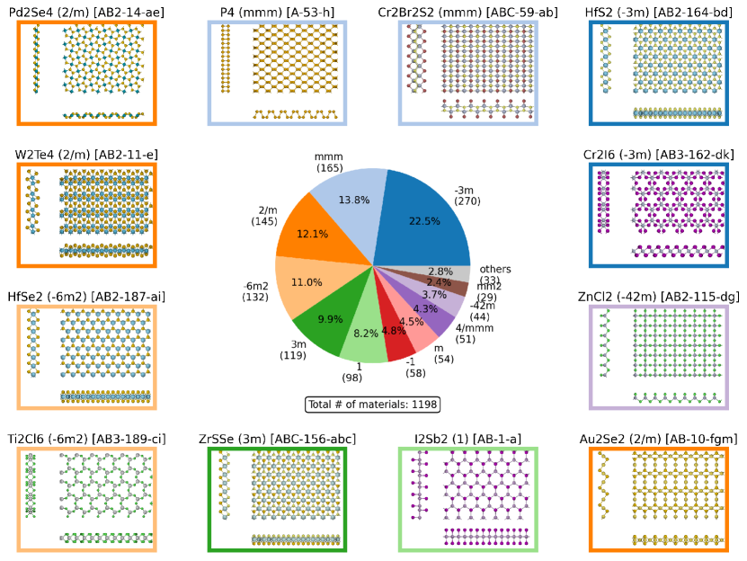
As shown by Neumann more than one century ago, the symmetries of any physical property of a material must include the symmetry operations of the point group to which the crystalline lattice belongs Neumann and Meyer (1885). Fig. 1 provides an overview of the 1198 thermodynamically and dynamically stable materials in C2DB grouped according to their point group symmetry, with the latter obtained from the Spglib library Togo and Tanaka (2018). Some specific examples of materials are shown with their point group indicated by the color of the frame. The selected materials represent some of the most interesting anisotropic 2D materials identified in this work and discussed in the following.
From Fig. 1, we make the following general observations:
-
•
Materials with trigonal symmetry, that is, materials belonging to the point groups -3m, 3m, -3, 3, 32 in the international notation111Note that we will substitute the common overline notation with a dash (that is, we will use instead of ), are the most frequently occurring ( of the total). These include, among others, TMDCs in the 1T phase such as HfS2 Xu et al. (2015), group IV monolayers Zhu et al. (2015), hydrogenated graphene (i.e. graphane Elias et al. (2009)), MXY Janus structures Lu et al. (2017); Fülöp et al. (2018); Riis-Jensen, Manti, and Thygesen (2020) such as ZrSSe, and monolayer magnetic materials such as CrI3 Huang et al. (2017).
-
•
Monoclinic materials (groups 2, m, 2/m) account for 18% of the total. They include TMDCs in the 1T’ phase, such as WTe2 Tang et al. (2017), TiS3 Island et al. (2014, 2015), and the pentagonal PdSe2 Oyedele et al. (2017). Of the 219 monoclinic materials investigated in this work, 140 of them bear orthogonal structure, while the remaining 79 have an inclined crystal system.
-
•
The orthorhombic structures comprise 16% of the total (groups mmm, mm2). Notable examples are the highly anisotropic puckered phosphorene (that is, monolayer black phosphorus Li et al. (2014)) and puckered arsenene Kamal and Ezawa (2015). We also point out the magnetic ternary compound CrSBr, which has been recently exfoliated from the layered bulk structureTelford et al. (2020); Lee et al. (2020) and whose crystal prototype is largely recurrent in C2DB among orthorhombic structures.
-
•
Triclinic materials (groups 1, -1) account for 13% of the total. This group include materials with low symmetry, such as TMDC alloys Komsa and Krasheninnikov (2012); Xie (2015), the topological insulator SbI Song et al. (2014); Vannucci, Olsen, and Thygesen (2020), and other potentially exfoliable materials such as AuSe.
-
•
11% of structures have hexagonal point group symmetry (groups -6m2, 6/mmm). They include TMDCs in the H phase such as HfSe2, hexagonal boron nitride (hBN), graphene (which is the only stable representative of the point group 6/mmm) and other less common structures possessing 6-fold rotation symmetry such as TiCl3.
-
•
The remaining 8% correspond to tetragonal structures (groups -42m, 4/mmm) such as ZnCl2, which is predicted to be easily exfoliableMounet et al. (2018).
This set of 1198 known or potentially exfoliable/synthesizable materials forms the basis for the anisotropy analysis presented in this work.
III Results and discussion
III.1 Magnetic easy axis
Magnetic anisotropy is defined in a material as the dependence of its properties on the direction of its magnetization. The main manifestation of magnetic anisotropy is the existence of an easy axis, along which it takes the least energy to magnetize the crystal, and a hard axis, where it takes the most. In order to quantify the degree of anisotropy, the magnetic anisotropy energy (MAE) is defined, which accounts for the energy necessary to deflect the magnetization from the easy to the hard direction. In general, the MAE may have contributions from different features of a crystal such as strain or defects. In this work we will consider perfect crystals, wherein only the so-called magnetocrystalline anisotropy, given by the coupling of the lattice to the spin magnetic moment, contributes to the MAE.
In 2D materials magnetic anisotropy gains a special importance due to the Mermin–Wagner theorem Mermin and Wagner (1966), which prohibits a broken symmetry phase at finite temperatures. This means that for a magnetic order to emerge, the spin rotational symmetry has to be broken explicitly by magnetic anisotropy. This has attracted a wide interest on the topic in the recent years, both in the light of new fundamental questions Huang et al. (2017); Fei et al. (2018); Zhang et al. (2015a); Lado and Fernández-Rossier (2017); Torelli and Olsen (2018); Torelli, Thygesen, and Olsen (2019) and applications Gong and Zhang (2019); Cardoso et al. (2018); Zhong et al. (2017); Burch, Mandrus, and Park (2018); Wang et al. (2018).
In this work we will focus on the in-plane MAE and define the and axes to span the atomic plane of the material. We define the in-plane MAE, , as:
| (1) |
where and are the electronic energies including spin-orbit coupling (SOC) with magnetization parallel to the and axes, respectively. In the electronic structure code GPAW, SOC is added non self-consistently on top of a converged PBE calculation as described in Ref. Olsen, 2016. This method yields very accurate results, as evidenced, for instance, by the excellent agreement of MoS2 SOC-induced band splitting with other first-principles approaches and with experiments Olsen (2016), or by the correct description of topological physics governed by SOC Olsen et al. (2019); Vannucci, Olsen, and Thygesen (2020). The MAE obtained with this method has been used in the calculation of critical temperature of magnetic 2D materials, providing good agreement with experiments Torelli and Olsen (2018); Torelli, Thygesen, and Olsen (2019).
Let us note that the definition of and axes is of course arbitrary. In C2DB, the axis is systematically chosen to be parallel to one of the lattice vectors, with the axis orthogonal to it. All properties are then calculated with respect to this reference frame. With this choice, the anisotropy is assessed with respect to the high symmetry axes for most of the materials in C2DB, except only for low symmetric obliques structures such as the ones in point group 1 and -1 (which represent only a 13% of the total). For such cases, the degree of anisotropy for some properties might be slightly underestimated.
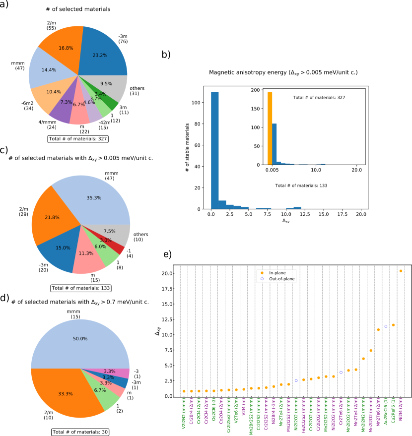
In Figure 2 we show the distribution of the magnetic materials in the C2DB database, sorted by their point group symmetry and the value of their in-plane magnetic anisotropy . In comparison with Fig. 1, we find a similar landscape once we filter for ferromagnetic (FM) or anti-ferromagnetic (AFM) materials, as shown in Fig 2a. This indicates that being magnetic or not is not strongly correlated to the point group, but to the presence of magnetic atoms in the structure. However, once anisotropy comes into play we do observe, in Fig 2b, important structural features that condition it. In fact, one can expect a magnetic easy axis to appear in the direction where magnetic atoms are packed more loosely, creating an anisotropy in the magnetic properties. For example, as we set a very low (0.005 meV/unit cell) threshold for , all hexagonal and tetragonal point groups vanish and only point groups not restricting the in-plane perpendicular directions by symmetry hold an in-plane magnetic anisotropy. Another feature we observe from Figure 2c, is the prevalence of the orthorhombic (mmm) and, to a lower degree monoclinic (2/m), systems with crystals of mmm point group symmetry representing over 35 of the materials with a low threshold. When we increase the threshold to 0.7 meV/unit cell we see that the trend is enhanced: mmm dominates with half of the materials and 2/m comprises a third of the materials (Figure 2d). The materials above this threshold are classified and sorted according to their anisotropy in Figure 2e. We see that both FM and AFM magnetic orders are equally represented, indicating little influence of the type of magnetic order on the anisotropy. In Figure 2e we also show the direction of the magnetic easy axis, indicated by a full orange marker if it lies within the plane and an empty blue one if it is oriented out-of-plane. It is clear that most of the selected anisotropic materials indeed present an in-plane easy axis.
Among the 113 materials with >0.005 meV/unit cell we find that the ternary compound structure prototype of orthorhombic symmetry ABC-59-ab Haastrup et al. (2018) is the most frequently occurring with 47 entries (see CrSBr in Fig. 1 for an example of this structure). The main reason for this might be the mentioned lack of symmetry between the and directions in the plane, along with the fact that it is more likely to contain a magnetic atom due to its ternary nature (most other crystals in C2DB are binary). To the best of our knowledge, the only 2D material from this group that has been successfully synthesized and exfoliated is CrSBr, whose FM order down to the monolayer limit has been very recently confirmed in experiments Telford et al. (2020); Lee et al. (2020). We note that several materials bearing the very same structure prototype are listed as easily exfoliable in Ref Mounet et al., 2018, e.g. CrOBr, CrOCl, FeOCl, VOBr and VOCl. Finally, the monoclinic T’ phase of transition metal dichalcogenides occurs 15 times, followed by the trigonal MoS2 Kappera et al. (2014) type with 10 occurrences.
We also cross-checked the rest of our selected anisotropic materials against the list of exfoliable 2D materials in Ref Mounet et al., 2018. We found, out of the 113 materials with >0.005 meV/unit cell, over 20 materials whose stoichiometry match entries in the list of exfoliable materials. Among these, perhaps the most promising material with regard to a potential experimental realization is the AFM T’ di-halide V2I4, which lies at the convex hull according to the C2DB database Haastrup et al. (2018). V2I4 shows an in-plane magnetic easy axis and meV/unit cell, that competes with the highest out-of-plane anisotropies known to date Torelli and Olsen (2018). In addition, we find several materials that are only a few meV above the convex hull and show remarkably high anisotropies. Among these the AFM Ni2I4 compound stands out with an exceptional in-plane anisotropy of over 20 meV/unit cell and an in-plane easy axis. Other materials in the same stability category, such as Ni2Br4, Co2O4 and CrBr2, also show large values and are listed in Table 1.
| Sym. | Mag. | (meV) | Lowest monolayer? | (meV/unit c.) | |
| Cr2Br4 | P21/m | FM | 54.4 | No | 0.79 |
| Co2O4 | C2/m | FM | 7.1 | No | 0.94 |
| V2I4 | Pm | AFM | 0.0 | Yes | 1.09 |
| Ni2Br4 | Pm1 | AFM | 8.8 | No | 1.55 |
| Ni2I4 | C2/m | AFM | 10.3 | No | 20.40 |
III.2 Elastic response and auxetic effect
The elastic response of 2D materials to strains and deformations is usually expressed in terms of the Young modulus and Poisson ratio Akinwande et al. (2017); Androulidakis et al. (2018). The former measures the response along a direction that is parallel to the applied strain, while the latter describes how the material reacts along orthogonal directions. For anisotropic materials, both the Young modulus and the Poisson ratio depend on the directions of stresses and strains. Assuming that the 2D material lies in the plane, and neglecting the elastic response along the out-of-plane axis , we will denote the axis-dependent Young modulus with , . Similarly, the coefficient relating the stress along the axis to an applied strain in the perpendicular direction will be quantified by the Poisson ratio , with .
More generally, the elastic response of a continuous 2D medium is quantified in terms of the 2D stiffness tensor , which is a linear map between the strain tensor and the stress tensor Landau and Lifshitz (1970):
| (2) |
Here we have , since we restrict to in-plane stresses and strains. A generic matrix element represents the component of the stress acting on a plane perpendicular to the direction, while the strain components are given by in terms of the infinitesimal deformations .
Being a linear map between two 2nd rank tensors, the stiffness tensor is naturally a 4th rank tensor. However, one can make use of the symmetric properties of both and at equilibrium to write both of them as one-dimensional vectors, namely
| (3) | ||||
| (4) |
Such a notation is often called Voigt notation. Then, the stiffness tensor becomes a 2nd rank symmetric tensor with only 6 independent components,
| (5) |
We will restrict the following analysis to the class of orthotropic materials, that is, materials having three mutually-orthogonal planes of reflection symmetry. In such a case, the stiffness tensor takes the form
| (6) |
In practice, this means that we restrict attention to materials where the shear deformations are decoupled from and stresses. This allows us to straightforwardly relate the components of the stiffness tensor to the in-plane Young modulus and in-plane Poisson ratio via the following relations:
| (7a) | ||||
| (7b) | ||||
| (7c) | ||||
| (7d) | ||||
In C2DB, each component of the 2D stiffness tensor is calculated by straining a material along a given direction ( or ) and calculating the forces acting on the unit cell after relaxing the position of the atoms within the fixed unit cell Haastrup et al. (2018). To restrict to orthotropic materials only, we have discarded all materials whose stiffness tensor components or exceed a certain tolerance , which we set to N/m. With this method, we have obtained a subset of 555 materials (roughly 50% of all the stable materials) that we analyze in the following.
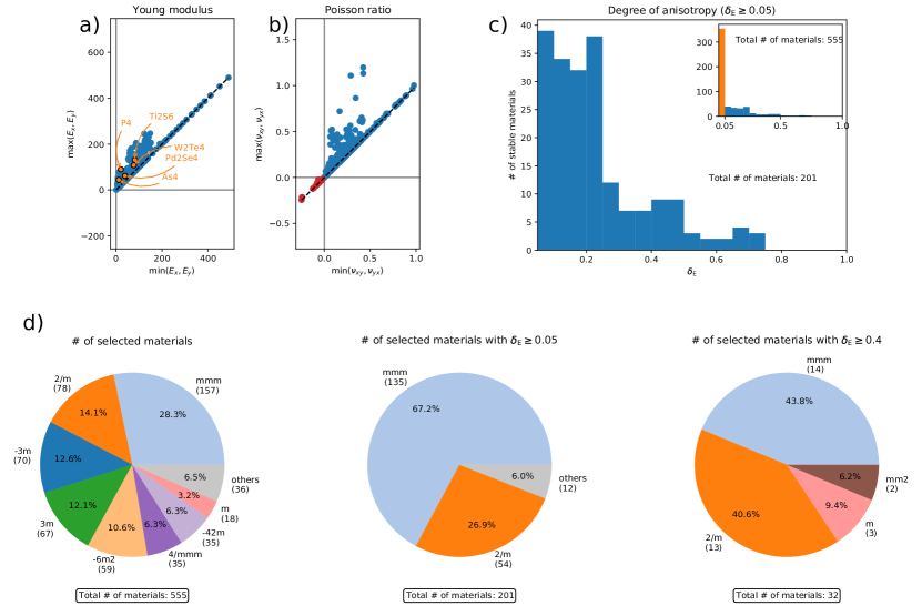
In Fig. 3a we show an overview of the direction-dependent Young modulus for all orthotropic and stable materials in C2DB. We plot against , which means that all data point lying outside the diagonal represent a material with anisotropic elastic properties. Well known anisotropic structures such as WTe2, PdSe2, TiS3, P4 and As4 are all identified by this method, while hundreds of unexplored anisotropic materials are predicted as well. In Fig. 3b we use a similar method to show the anisotropy of the Poisson ratio. While this does not add much information with respect to panel a — since , as one can easily infer from Eqs. 7 — we notice that Poisson ratios can also take negative values, differently from the Young modulus. In such a case, a material stretched (or compressed) along the direction will also expand (shrink) along the perpendicular direction, a quite counterintuitive property called auxetic behavior Akinwande et al. (2017); Jiang, Kim, and Park (2016). We will investigate such cases in more detail in the following.
To describe elastic anisotropy in a more quantitative manner, we define an elastic anisotropy degree (or anisotropy parameter) for each material as
| (8) |
Such a parameter will be always bounded between 0 and 1, with signifying a perfectly isotropic materials while for an extremely anisotropic medium.
In Fig. 3c we show the distribution of the elastic anisotropy degree for all materials having (corresponding to a difference of at least 10% between and Young modulus), with the inset showing the full distribution including materials with . We notice that more than one third of the selected materials (201 out of 555) show an elastic anisotropy exceeding this threshold value, while 162 of them exceed the value (signifying a difference of roughly 20% or more between and ) and 32 of them show a highly anisotropic elastic behaviour with .
The distribution of point groups corresponding to different threshold values for is shown as a series of pie charts in Fig. 3d. On the left, we plot the distribution of point groups for all 555 selected materials. A comparison with Fig. 1 shows that our choice of selecting only orthotropic materials tends to favor orthorhombic structures (especially group mmm) with respect to trigonal ones, while the proportions between remaining point groups remain basically unaffected. However, when selecting all materials with at least 10% of difference between and (, in the middle), the proportions change drastically, with all trigonal and hexagonal groups suppressed in favor of orthorhombic and monoclinic structures. This shows that symmetric crystal structures such as the ones of TMDCs in the H and T phase, graphene and hBN are generally isotropic, with little difference in the elastic properties along and directions. On the other hand, TMDCs in the distorted T’ phase (such as WTe2), pentagonal structures (PdSe2) and puckered layers (phosphorene) stand out for their markedly anisotropic elastic properties due to their asymmetric crystal lattice.
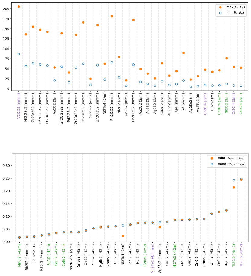
When restricting to highly anisotropic materials having , monoclinic and orthorhombic structures share exactly 50% of the total each. The Young moduli of these 32 structures are plotted in the top panel of 4, sorted from lowest to highest value of . Besides known structures such as phosphorene (P4) and puckered arsenene (As4), we find many new stable structures with exceptionally high elastic anisotropy. Four out of the first six materials are compounds of the form CrX2 (with X a halogen element) in both the AFM and FM magnetic state, which also stand out for their markedly anisotropic magnetic behavior as described previously. These are, however, not the most stable structures with the same constituent elements, since they all have a competing phase of the form CrX3 with a more favorable formation energy (one of them is shown in Fig. 1). However, this is not the case for the monoclinic structures AuSe and AuTe, which represent the most stable phase of their respective elements. One of them (AuSe, which is shown in Fig. 1 as well) has also been identified as an easily exfoliable materials by independent work of Mounet et al. Mounet et al. (2018), making this one of the most appealing material for anisotropic elastic applications found in this work. We also note that puckered compounds GeS and GeSe seem also to be easily exfoliable from their respective three-dimensional parent structures, which is again confirmed in the literature Mounet et al. (2018).
Finally, it is worth mentioning the presence of several entries in the structural prototype ABC-59-ab (especially Hf- and Zr-based compounds), whose relevance has already been discussed in the previous section. We note that Ref. Mounet et al., 2018 lists HfNBr, ZrNBr and ZrNI as easily exfoliable layered materials. We find a relatively low elastic anisotropy degree for ZrNI, but we suggest that materials with much higher elastic anisotropy such as HfBrX and ZrBrX (with X = S, Se) should in principle be available by susbtitution of Nitrogen with an element from the halogen group.
Let us now come back to the subset of materials showing a negative in-plane Poisson ratio, that is the ones highlighted with red markers in Fig. 3b. The auxetic effect is not necessarily associated to anisotropy as both Poisson ratios and can take negative values without necessarily being different from each other. Indeed, such an effect does not originate from the material having a different elastic response along orthogonal axes, but rather from the presence of special re-entrant structures or rigid blocks linked by flexible hinges in the crystalline structure, that can compress or extend in counter-intuitive fashions. Nevertheless, our framework allows for the systematic search of novel 2D materials with negative Poisson ratio, which itself is an active field of research Jiang, Kim, and Park (2016). Moreover, Poisson ratios of anisotropic materials can take arbitrarily large values (positive or negative), differently from ordinary isotropic media Ting and Chen (2005).
In the bottom panel of Fig. 4 we plot the Poisson ratios of the 31 stable materials in C2DB showing auxetic behavior, sorting from lowest to highest value of . The largest negative Poisson ratio is found for TiCl3 in the hexagonal crystal structure (shown in Fig. 1), with both AFM and FM magnetic configurations. Once again, this is not the most stable phase for such a compound, which reaches the lowest energy configuration when arranged in a trigonal phase, in the same crystal prototype as the ferromagnetic insulator CrI3 Huang et al. (2017).
There are several interesting candidates among the materials with tetragonal structure. In particular, materials with stoichiometry AB2 in point group -42m, such as the case of ZnCl2 shown in Fig. 1, represent a large majority of stable auxetic materials in C2DB. Notable examples are metal di-halides involving Co, Mn, or Fe as the metallic element. Such materials are all exfoliable from a 3D parent compound with trigonal point group Mounet et al. (2018), but their tetragonal phases generally have total energies that are comparable or even lower than the trigonal monolayer phase (which is also present in C2DB). A second notable example is given by group 12 di-halides involving Zn, Cd, and Hg, for which the tetragonal auxetic structure turns out to be the most stable phase. Interestingly, both HgI2 and ZnCl2 are reported as easily exfoliable materials by Mounet et al.Mounet et al. (2018), making these two materials very appealing candidates for novel auxetic 2D materials. We also note that MnTe, AgBr, and GeO2 all seem to have total energies very close to the convex hull, and thus also belong to the set of predicted stable auxetic monolayers.
Let us note that a significant majority of known auxetic 2D structures display negative Poisson ratio in the out-of-plane direction Liu et al. (2019); Kong et al. (2018); Gomes, Carvalho, and Castro Neto (2015); Jiang and Park (2014); Du et al. (2016), while only very few materials were previously predicted to exhibit in-plane auxetic response Yu, Yan, and Ruzsinszky (2017); Qin and Qin (2020). Ref. Yu, Yan, and Ruzsinszky, 2017 reports negative Poisson ratio for monolayers of groups 6–7 transition-metal dichalcogenides (MX2 with M=Mo, W, Tc, Re and X=S, Se, Te) in the 1T-phase. We do find a negative in C2DB for all of them, but they have low dynamical and thermodynamical stability, and therefore are not identified by our analysis.
III.3 Effective masses
Monolayer 2D materials with a finite band gap can display large anisotropies in the effective masses along two orthogonal directions. This makes them appealing for highly directional-dependent transport, with applications in anisotropic field-effect transistors, polarization-sensitive detectors and non-volatile memory devices among others Jin, Li, and Yang (2015); Liu et al. (2015); Zhang et al. (2016); Liu et al. (2020); Wang et al. (2019, 2015).
In C2DB, effective masses for conduction and valence bands are calculated for all materials having a finite band gap greater than 0.01 eV at the PBE level. We define the effective mass, , from the curvature, , at the band maximum (minimum) for valence (conduction) bands as . To determine the curvature we start from a self-consistent ground state calculation performed at a -point density of 12 Å-1. From these -points a preliminary band extremum is found and a second, non-self-consistent calculation is performed with higher density of -points centered around the preliminary extremum. Then, from these values a final extremum is determined and the energies for a number of -points spaced very closely around the extremum are calculated non-self-consistently. The -points used for the first refinement step are by default chosen to lie in a sphere around the extremum with a radius of 250 meV (for a mass of 1) and the same number of -points as the original calculation (but at least 19). The last refinement uses a 1 meV sphere and 9 points. The points calculated in the final refinement step are used to determine the curvature. We first do a fit to a second order polynomial to determine a preliminary extremum. Then we perform a fit to a third order polynomial and find the new extremum, unless the optimization algorithm diverges (as may happen for third order polynomials) in which case we revert to the original fit. We have found that the third order polynomial fit does provide an improvement to the description of the band extremum and in some cases is necessary, e.g. in the presence of parabolic bands crossing as in Rashba splitting. From the fit we find the curvature at the extremum and the mass is calculated as .
To measure the presence of anisotropic effects in the effective masses, we define the parameters
| (9a) | ||||
| (9b) | ||||
where:
-
•
is the effective electron mass calculated along the direction around the conduction band minimum;
-
•
is the effective hole mass calculated along the direction around the valence band maximum.
Unfortunately, getting a very accurate value for the effective masses in a fully automated fashion turns out to be a quite challenging task, with some fits being not accurate enough, or picking a wrong sign for the electron or hole mass in the case of a particularly heavy effective mass. We therefore remove all materials having , with the free electron mass, and materials with extremely high ratio . We stress that these threshold values are arbitrary. They have been primarily chosen so that we discard all wrong results, while also keeping the highly anisotropic materials with accurate results into the analysis as much as possible.
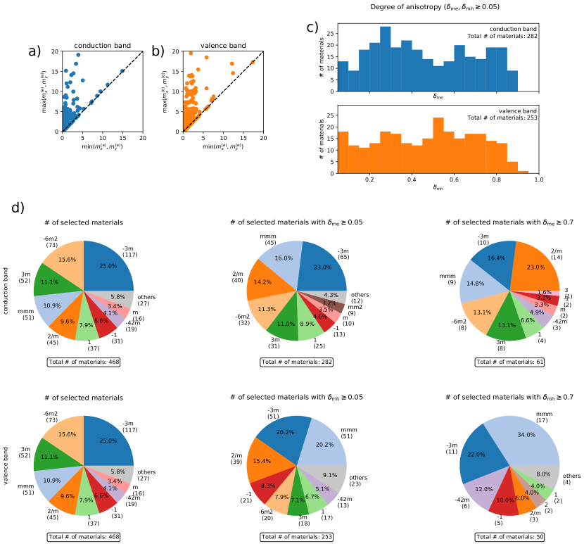
The C2DB database contains 574 dynamically and thermodynamically stable materials with a PBE band gap greater than 0.01 eV, of which 106 fall outside the range of validity described above. This leaves us with a total of 468 materials, whose effective electron and hole masses are shown as a scatter plot in Fig. 5a and 5b. We find a rather large set of materials with anisotropic effective masses, as one can immediately notice from the large number of points falling outside the main diagonal. Indeed, as shown in Fig. 5c, 60% of the selected materials (282 out of 468) show a difference of at least 10% between electron effective masses, while 54% of them (253 out of 468) have at least 10% of difference between hole effective masses. Moreover, a quite large fraction of materials have extremely high values of or as compared with the case of elastic anisotropy in Fig. 3c.
When considering the distribution of point groups for materials with effective masses anisotropy, a quite different behavior with respect to previous cases emerges. First, as shown in the left column of Fig. 6, let us notice that the restriction to semiconductors with a band gap of at least 0.01 eV removes many structures in the orthorhombic (mmm) and monoclinic (2/m) groups, while favoring structures with trigonal (-3m, 3m) and hexagonal (-62m) symmetry with respect to the general case shown in Fig. 1. More importantly, we notice that these structures are not filtered out even when we select materials with increasingly high effective masses anisotropy ( in the middle, on the right). This means that, despite their structural symmetry, materials such as TMDCs in the T and H phase and Janus structures display a quite strong anisotropy in the effective masses. One should bear in mind that we only calculate the curvatures of valence and conduction bands in one particular valley. While these are not bound to symmetries of the crystal, the overall transport properties (such as, for instance, the mobility) are determined by adding up contributions from all valleys, which in the end cancels out any anisotropic effect and restores the Neumann principle. However, it’s worth noting that transport properties of a single anisotropic valley should in principle be accessible in experiments with valley-selection techniques such as circularly polarized optical excitation and gating Cao et al. (2012); Mak et al. (2014); Lee, Mak, and Shan (2016)
For the case of electron effective masses, we find that 61 stable materials have a rather high anisotropy degree . While this group is dominated by monoclinic structures in the 2/m point group (mostly TMCD in the distorted T’ phase) we find a rather large set of triclinic structures which sum up to roughly one third of the total, and a significant 13% of share for hexagonal structures. The situation is different for the case of hole effective masses, where orthorhombic structures represent a 34% of the 50 materials with . However, we still find that 22% of structures are in a trigonal point group as well.
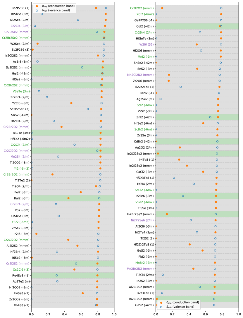
We have reported all the 101 structures with or greater that 0.7 in Fig. 6, with 10 of them having both parameters above the threshold value. Among this group, we notice a recurrent presence of Hafnium, Bismuth and Antimony-based Janus structures, and Chromium based compounds (especially Chromium halides, which also bear elastic and magnetic anisotropy). Most importantly, we find few materials that have already been exfoliated down to monolayer thickness in experiments, including four Hafnium and Zirconium-based TMDC in the stable T phase and the already mentioned FM compound CrBrS. We also point out the presence of monolayers SbI3, BiClTe, SbITe, and other ternary compounds in the crystal prototype ABC-59-ab (point group mmm) such as CrBrO and CrClO, which all seem to be easily exfoliable from the layered 3D parent bulk structure Mounet et al. (2018). Finally, we note that the direct or indirect character of the band gap does not seem to be relevant for attaining high anisotropy in the effective masses. Indeed, we find 18 out of 101 highly anisotropic materials with direct gap (that is 18%), which is not dramatically different from the total fraction of semiconductors and insulators with direct gap among the 468 materials considered in this analysis (29 %).
A list of experimentally available or easily exfoliable materials with highly anisotropic effective masses is presented in Table 2, where we also report three experimentally available materials and one easily exfoliable material having (namely TiS3, SnSe2, GaTe, AuSe). We also include additional structures that can be obtained from this subset by replacing a constituent element with atoms from the same group. This a relevant case for Janus monolayer, which can be obtained from already available structures by stripping off an outer layer of chalcogen atoms and substituting them with an element from the same family Lu et al. (2017). A similar method is likely to be applicable to halogen and chalcogen atoms in ternary orthorhombic compounds. For each entry of Table 2, we have double-checked the accuracy of the parabolic fit.
| material | pointgroup | Ref. (exp.) | exfol. from bulk | ||
| CrBrS (AFM) | mmm | 0.89 | 0.94 | Ref. Lee et al.,2020 | yes |
| W2Se4 | 2/m | 0.07 | 0.88 | Ref. Chen et al.,2018 | |
| CrBrS (FM) | mmm | 0.85 | 0.84 | Ref. Lee et al.,2020 | yes |
| HfSe2 | -3m | 0.85 | 0.00 | Ref. Aretouli et al.,2015 | yes |
| Ti2CO2 | -3m | 0.83 | 0.00 | Ref. Melchior et al.,2018 | |
| HfS2 | -3m | 0.81 | 0.00 | Ref. Xu et al.,2015 | yes |
| ZrSe2 | -3m | 0.81 | 0.00 | Ref. Mañas-Valero et al.,2016 | yes |
| Re4Se8 | -1 | 0.80 | 0.30 | Ref. Zhang et al.,2016 | yes |
| SnS2 | -3m | 0.50 | 0.78 | Ref. Sun et al.,2012 | yes |
| ZrS2 | -3m | 0.75 | 0.00 | Ref. Zhang et al.,2015b | yes |
| PbI2 | -3m | 0.00 | 0.72 | Ref. Zheng et al.,2019 | yes |
| Ti2S6 | 2/m | 0.60 | 0.52 | Ref. Island et al.,2014 | yes |
| SnSe2 | -3m | 0.55 | 0.00 | Ref. Park et al.,2016 | yes |
| Ga2Te2 | -6m2 | 0.51 | 0.37 | Ref. Pozo-Zamudio et al.,2015 | yes |
| CrBrO (AFM) | mmm | 0.37 | 0.84 | yesHaastrup et al. (2018); Mounet et al. (2018) | |
| CrClO (AFM) | mmm | 0.83 | 0.79 | yesHaastrup et al. (2018); Mounet et al. (2018) | |
| CrBrO (FM) | mmm | 0.25 | 0.83 | yesHaastrup et al. (2018); Mounet et al. (2018) | |
| CrClO (FM) | mmm | 0.45 | 0.81 | yesHaastrup et al. (2018); Mounet et al. (2018) | |
| I6Sb2 | -3m | 0.01 | 0.80 | yesHaastrup et al. (2018) | |
| Au2Se2 | 2/m | 0.65 | 0.26 | yesHaastrup et al. (2018); Mounet et al. (2018) | |
| material | pointgroup | obtainable via substitution | |||
| CrBrSe (AFM) | mmm | 0.94 | 0.92 | from CrBrSMounet et al. (2018) | |
| CrIS (FM) | mmm | 0.93 | 0.73 | from CrBrSMounet et al. (2018) | |
| BrSbSe | 3m | 0.90 | 0.13 | from ISbTe Mounet et al. (2018) | |
| CrISe (AFM) | mmm | 0.89 | 0.80 | from CrBrSMounet et al. (2018) | |
| CrBrSe (FM) | mmm | 0.88 | 0.88 | from CrBrSMounet et al. (2018) | |
| CrIS (AFM) | mmm | 0.79 | 0.53 | from CrBrSMounet et al. (2018) | |
| CrIO (FM) | mmm | 0.08 | 0.79 | from CrBrOMounet et al. (2018), CrClOMounet et al. (2018) | |
| HfSeTe | 3m | 0.79 | 0.01 | from HfS2Xu et al. (2015), HfSe2Aretouli et al. (2015) | |
| ZrSSe | 3m | 0.75 | 0.00 | from ZrS2Zhang et al. (2015b), ZrSe2Mañas-Valero et al. (2016) | |
| CrIO (AFM) | mmm | 0.15 | 0.58 | from CrBrOMounet et al. (2018), CrClOMounet et al. (2018) | |
III.4 Polarizability
The polarizability of a material relates the induced electric dipole moment density to an applied electric field to linear order.Le Ru and Etchegoin (2008). For 2D materials, this relation takes the form:
| (10) |
where is the induced polarization in the material averaged over the area of the unit cell, is the the applied electric field, and is the polarizability.Haastrup et al. (2018).
In general, the polarizability can be split into a contribution from the electrons, , and a contribution from the lattice, . Since the characteristic response time of the electrons is much faster than that of the lattice, the relevance of the two contributions depends on the timescale of the considered problem. For optical processes involving electromagnetic waves with frequency well above the characteristic phonon frequency of the lattice, only the electronic polarizability is relevant and we can write . On the other hand, for processes involving infrared light, the lattice response must be considered as well and can in some case even dominate the electronic response.
The polarizability determines the degree of dielectric screening in a material and as such it sets the strength of Coulomb interaction between charged particlesHüser, Olsen, and Thygesen (2013); Tian et al. (2020). It thereby governs several of the unique properties that made 2D materials famous over the last decade Novoselov et al. (2004); Castro Neto et al. (2009); Mak et al. (2010) including excitons, plasmons, and band gap renormalization effectsThygesen (2017). In this context, the in-plane anisotropy of 2D materials has attracted significant interest since the synthesis of few-layer black phosporous (P4) in 2014 Li et al. (2014); Liu et al. (2014); Xia, Wang, and Jia (2014). For example, the anisotropic optical absorption (essentially the imaginary part of the electronic polarizability) makes the material act as a linear polarizerWy et al. (2014), which finds applications in diverse fields such as liquid-crystal displays, medical applications, or optical quantum computers Knill, Laflamme, and Milburn (2001); Zeng et al. (2009). In addition, other fundamental properties, such as the electron-phonon coupling and electron-hole interactions, are influenced by an anisotropic polarizability resulting in formation of quasiparticles, e.g. polarons, excitons, trions, with unconventional shapes and dispersion relations.Ling et al. (2016); Li et al. (2015); Wy et al. (2014); Xu et al. (2016); Yang et al. (2015); Deilmann and Thygesen (2018); Gjerding et al. (2020).
In the C2DB the electronic polarizability is calculated within the random phase approximation (RPA) Langreth and Perdew (1975); Olsen and Thygesen (2013) using PBE wave functions and eigenvalues, see Ref Haastrup et al., 2018 for further details. To keep the discussion general we focus here on the polarizability in the static () and long wavelength () limits. As a measure of the degree of anisotropy we adopt the parameter defined above and define
| (11) |
with for the electronic and lattice polarizability respectively.
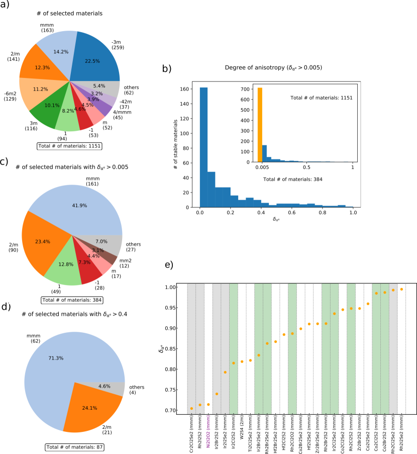
In figure 7 panels (c) and (d) we show the statistical distribution of the materials with electronic polarizability anisotropy above 0.005 and 0.4, respectively. For reference, the distribution of all the materials for which the polarizability has been calculated is shown in panel (a), and the materials are classified according to point group symmetry as usual. As the threshold is increased we see the same trend as for the magnetic, elastic, and effective masses anisotropies, namely, the orthorhomic mmm point group followed by the monoclinic 2/m becomes increasingly dominant. Both the trigonal and tetragonal phases disappear from the distribution already for >0.005. The othorhombic mmm group is particularly ubiquitous among the materials with high , surpassing 70 of the remaining materials already at a moderate threshold of > 0.4. In figure 7e we show the materials with the largest anisotropies found in the range > 0.7. We note that our analysis correctly identifies the known in-plane anisotropic compounds such as P4 Li et al. (2014) (phosphorene), As4 Kamal and Ezawa (2015) (arsenene), MoS2 (in the T’ phase) and WTe2 Tang et al. (2017) among others.
The materials with the highest are ternary compounds and therefore more challenging to realize experimentally than the more common binary 2D materials, a notable exception being the recently synthesised Cs2Br2S2 Lee et al. (2020), mentioned above, which has in addition a high electronic polarizability anisotropy. Regarding binary compounds, several of the materials with large have been predicted to be exfoliable from known parent bulk materials Mounet et al. (2018). Among our anisotropic materials that match the stoichiometry of the materials listed in Mounet et al., 2018 as easily exfoliable, the most promising of these are listed in Table 3.
| Sym. | (meV) | Lowest monolayer? | ||
| Cs2Br2S2 Lee et al. (2020) | Pmmm | 0.0 | Yes | 0.41 |
| W2Se | P/m | 91.7 | No | 0.47 |
| Zr2I4 | P/m | 0.0 | Yes | 0.51 |
| Mo2Se4 | P/m | 109.4 | No | 0.54 |
| Zr2Cl4 | P/m | 31.9 | No | 0.60 |
| Ti2Cl4 | P/m | 0.0 | Yes | 0.65 |
| W2S4 | P/m | 177.9 | No | 0.82 |
We highlight the experimentally known ternary compound Cs2Br2S2 among the easily exfoliable materials from Table 3, presenting a high optical polarizability anisotropy of >0.41. Among the compounds not known yet experimentally we highlight two in the table, that have >0.65 and >0.5, respectively: Ti2Cl4 and Zr2I4. We stress that , for instance, implies that the polarizability in one direction of the plane is 4.7 times larger than in the other direction. Consequently, these materials are very promising candidates for anisotropic optical applications such as light polarizers.
The lattice or infrared polarizability is calculated in the C2DB database only for materials meeting the requirements of high stability and band gap > 10 meV, which represent about 15% of the materials in the database. Hence we will limit our analysis to extracting the most promising individual materials, since a statistical analysis would not be representative of the real distribution of the materials in the database. In Figure 8 we show all 16 materials with >0.2. As it is the case with the rest of properties, we find several materials with a significant anisotropy. For instance, the monolayer Sn2Te2 has a value 0.45, is at the bottom of the convex hull combining Sn and Te among monolayers and is considered to be easily exfoliable Mounet et al. (2018). This makes it a very interesting material for further experimental and theoretical exploration. We find other materials whose stoichiometry matches easily exfoliable entries in Ref. Mounet et al., 2018 among those with >0.25, and are listed in Table 4. Taking into account that these promising materials are selected among only a little fraction of the entire C2DB database, we anticipate that there are a large amount of promising infrared anisotropic materials in the database yet to be discovered.
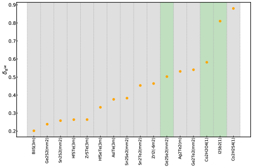
| Sym. | (meV) | Lowest monolayer? | ||
| Sn2S2 | Pmn | 42.6 | No | 0.26 |
| Sn2Se2 | Pmn | 42.9 | No | 0.38 |
| Sn2Te2 | Pmn | 62.9 | Yes | 0.45 |
| ZrI2 | Pm2 | 27.0 | No | 0.46 |
| Ge2Se2 | Pmn | 24.9 | No | 0.50 |
IV Conclusions
In this work, we have analyzed the presence of anisotropic behavior among more than one thousand 2D materials predicted to be stable in the C2DB database Haastrup et al. (2018). Specifically, we have identified materials with in-plane magnetic anisotropy, anisotropic Young’s modulus and/or negative Poisson ratio, anisotropic effective masses, and anisotropic polarizabilities.
Consistent with the Neumann principle, we have found that there are two main features in the C2DB database that favour anisotropy, namely (i) a lower symmetry and (ii) a larger number of constituent elements. In addition, our analysis satisfactorily captures the specific symmetry requirements of each anisotropy type: elastic and polarizability anisotropies, derived from second order tensors, are forbidden for trigonal, tetragonal or hexagonal compounds; the magnetic anisotropic materials do not include hexagonal and tetragonal groups, and the effective mass anisotropy is allowed for all symmetry groups in the database. Several of the materials identified in this study outperform the known 2D materials in terms of anisotropic figures of merit and are predicted to be stable and/or exfoliable from known parent bulk crystalsMounet et al. (2018), providing useful guidelines for future experimental investigations.
The most prominent material class resulting from our analysis is the ternary orthorhombic compound prototype ABC-59-abHaastrup et al. (2018). This material class combines three different atomic species in a low symmetry structure, often resulting in strongly anisotropic properties. To the best of our knowledge, one of such materials (namely CrSBr) has been isolated in monolayer form very recently Lee et al. (2020), and further experimental efforts in this direction could hopefully be motivated by our work.
We find several binary monolayers with interesting anisotropic behaviors that are predicted to be stable and in some cases even predicted as easily exfoliable. A transition metal (in particular Ni, V, Cr, Os) combined with a halide in a low symmetry structure appears to be the best recipe for obtaining in-plane magnetic and elastic anisotropy. For instance, VI2 is an exfoliable and very stable compound with an in-plane magnetic anisotropy that competes with the highest out-of-plane anisotropies known to date. Moreover, there are multiple compounds with large predicted anisotropies, that match the stoichiometry of exfoliable materials and with similar total energies. Such materials could be stabilized under the right experimental conditions. Among them, we highlight anti-ferromagnetic Ni2I4, which has an exceptional in-plane anisotropy exceeding 20 meV/unit cell, that makes it a candidate for realization of high temperature in-plane 2D antiferromagnetism. Likewise, the chromium di-halides stand out for their markedly anisotropic behavior in the elastic response and effective electron and hole masses. Among the non-magnetic materials, we identify AuX (X=S, Se, Te) as a new class of potentially stable 2D materials with high anisotropy in several physical properties, with AuSe being reported as easily exfoliable in the literature.
On the other hand, transport properties of a single valley deserve to be mentioned separately, as they do not seem to be bound to the symmetries of the crystal lattice and could be experimentally accessed by means of circularly polarized light. Several TMDCs and Janus structures have highly symmetric crystal struture with trigonal symmetry but strong effective mass anisotropy, and we identify HfX2, ZrX2, and SnX2 (X = S, Se) as the most interesting monolayers for anisotropic transport applications already available in experiments, together with the above mentioned CrSBr. Moreover, new undiscovered structures with very low inter-layer binding energy such as SbI3, AuSe, and ternary magnetic compounds CrOBr and CrOCl display strong effective masses anisotropies.
Regarding the electronic polarizability, we also find a large amount of anisotropic materials, nearly all being ternary compounds of orthorhombic symmetry. In addition, some binary compounds, mostly involving a transition metal and a halide or a chalcogen, that are predicted to be easily exfoliable are identified and listed in the text. Finally, we also identified materials with interesting infrared polarizability anisotropy values among a smaller set of candidates in the C2DB. The most promising prospects for experimental realization are listed in the text.
Among the materials with negative Poisson ratios (so-called auxetic materials) identified in our study, we highlight HgI2 and ZnCl2, which are both predicted as easily exfoliableMounet et al. (2018), and MnTe, AgBr, and GeO2, which are predicted to be stable in their monolayer form.
Acknowledgements.
We thank Alireza Taghizadeh for useful discussions and suggestions. The research leading to these results has received funding from the European Union’s Horizon 2020 research and innovation program under the Marie Skłodowska-Curie grant agreement No. 754462. (EuroTechPostdoc). KST acknowledges funding from the European Research Council (ERC) under the European Union’s Horizon 2020 research and innovation programme (Grant No. 773122, LIMA). The Center for Nanostructured Graphene is sponsored by the Danish National Research Foundation, Project DNRF103.Data availability
The data that support the findings of this study are openly available online at the C2DB website C2D .
References
References
- Gjerding et al. (2017) M. N. Gjerding, R. Petersen, T. G. Pedersen, N. A. Mortensen, and K. S. Thygesen, “Layered van der Waals crystals with hyperbolic light dispersion,” Nature Communications 8, 320 (2017).
- Jacob, Alekseyev, and Narimanov (2006) Z. Jacob, L. V. Alekseyev, and E. Narimanov, “Optical hyperlens: far-field imaging beyond the diffraction limit,” Optics express 14, 8247–8256 (2006).
- Lu et al. (2014) D. Lu, J. J. Kan, E. E. Fullerton, and Z. Liu, “Enhancing spontaneous emission rates of molecules using nanopatterned multilayer hyperbolic metamaterials,” Nature nanotechnology 9, 48–53 (2014).
- Novoselov et al. (2004) K. S. Novoselov, A. K. Geim, S. V. Morozov, D. Jiang, Y. Zhang, S. V. Dubonos, I. V. Grigorieva, and A. A. Firsov, “Electric Field Effect in Atomically Thin Carbon Films,” Science 306, 666–669 (2004).
- Ci et al. (2010) L. Ci, L. Song, C. Jin, D. Jariwala, D. Wu, Y. Li, A. Srivastava, Z. Wang, K. Storr, L. Balicas, et al., “Atomic layers of hybridized boron nitride and graphene domains,” Nature materials 9, 430–435 (2010).
- Mak et al. (2010) K. F. Mak, C. Lee, J. Hone, J. Shan, and T. F. Heinz, “Atomically Thin : A New Direct-Gap Semiconductor,” Phys. Rev. Lett. 105, 136805 (2010).
- Li et al. (2014) L. Li, Y. Yu, G. J. Ye, Q. Ge, X. Ou, H. Wu, D. Feng, X. H. Chen, and Y. Zhang, “Black phosphorus field-effect transistors,” Nature nanotechnology 9, 372 (2014).
- Fei and Yang (2014) R. Fei and L. Yang, “Strain-Engineering the Anisotropic Electrical Conductance of Few-Layer Black Phosphorus,” Nano Letters 14, 2884–2889 (2014).
- Xia, Wang, and Jia (2014) F. Xia, H. Wang, and Y. Jia, “Rediscovering black phosphorus as an anisotropic layered material for optoelectronics and electronics,” Nat. Commun. 5, 4458 (2014).
- Wei and Peng (2014) Q. Wei and X. Peng, “Superior mechanical flexibility of phosphorene and few-layer black phosphorus,” Applied Physics Letters 104, 251915 (2014).
- Low et al. (2014) T. Low, R. Roldán, H. Wang, F. Xia, P. Avouris, L. M. Moreno, and F. Guinea, “Plasmons and Screening in Monolayer and Multilayer Black Phosphorus,” Phys. Rev. Lett. 113, 106802 (2014).
- Wang et al. (2015) L. Wang, A. Kutana, X. Zou, and B. I. Yakobson, “Electro-mechanical anisotropy of phosphorene,” Nanoscale 7, 9746–9751 (2015).
- Jain and McGaughey (2015) A. Jain and A. McGaughey, “Strongly anisotropic in-plane thermal transport in single-layer black phosphorene,” Sci Rep 5, 8501 (2015).
- Wang et al. (2015) X. Wang, A. M. Jones, K. L. Seyler, V. Tran, Y. Jia, H. Zhao, H. Wang, L. Yang, X. Xu, and F. Xia, “Highly anisotropic and robust excitons in monolayer black phosphorus,” Nature Nanotechnology 10, 517–521 (2015).
- Tian et al. (2016) H. Tian, Q. Guo, Y. Xie, H. Zhao, C. Li, J. J. Cha, F. Xia, and H. Wang, “Anisotropic Black Phosphorus Synaptic Device for Neuromorphic Applications,” Advanced Materials 28, 4991–4997 (2016).
- Yang et al. (2017) H. Yang, H. Jussila, A. Autere, H.-P. Komsa, G. Ye, X. Chen, T. Hasan, and Z. Sun, “Optical Waveplates Based on Birefringence of Anisotropic Two-Dimensional Layered Materials,” ACS Photonics 4, 3023–3030 (2017).
- Wang et al. (2020) C. Wang, G. Zhang, S. Huang, Y. Xie, and H. Yan, “The Optical Properties and Plasmonics of Anisotropic 2D Materials,” Advanced Optical Materials 8, 1900996 (2020).
- Ma et al. (2016) J. Ma, Y. Chen, Z. Han, and W. Li, “Strong anisotropic thermal conductivity of monolayer WTe2,” 2D Materials 3, 045010 (2016).
- Torun et al. (2016) E. Torun, H. Sahin, S. Cahangirov, A. Rubio, and F. M. Peeters, “Anisotropic electronic, mechanical, and optical properties of monolayer WTe2,” Journal of Applied Physics 119, 074307 (2016).
- Zhang et al. (2019a) Y.-J. Zhang, R.-N. Wang, G.-Y. Dong, S.-F. Wang, G.-S. Fu, and J.-L. Wang, “Mechanical properties of 1T-, 1T’-, and 1H-MX2 monolayers and their 1H/1T’-MX2 (M = Mo, W and X = S, Se, Te) heterostructures,” AIP Advances 9, 125208 (2019a).
- Zhang et al. (2019b) Q. Zhang, R. Zhang, J. Chen, W. Shen, C. An, X. Hu, M. Dong, J. Liu, and L. Zhu, “Remarkable electronic and optical anisotropy of layered 1T’-WTe2 2D materials,” Beilstein J. Nanotechnol. 10, 1745–1753 (2019b).
- Wang et al. (2020) C. Wang, S. Huang, Q. Xing, Y. Xie, C. Song, F. Wang, and H. Yan, “Van der Waals thin films of WTe2 for natural hyperbolic plasmonic surfaces,” Nature Communications 11, 1158 (2020).
- Island et al. (2014) J. O. Island, M. Buscema, M. Barawi, J. M. Clamagirand, J. R. Ares, C. Sánchez, I. J. Ferrer, G. A. Steele, H. S. J. van der Zant, and A. Castellanos-Gomez, “Ultrahigh Photoresponse of Few-Layer TiS3 Nanoribbon Transistors,” Advanced Optical Materials 2, 641–645 (2014).
- Island et al. (2015) J. O. Island, M. Barawi, R. Biele, A. Almazán, J. M. Clamagirand, J. R. Ares, C. Sánchez, H. S. J. van der Zant, J. V. Álvarez, R. D’Agosta, I. J. Ferrer, and A. Castellanos-Gomez, “TiS3 Transistors with Tailored Morphology and Electrical Properties,” Advanced Materials 27, 2595–2601 (2015).
- Kang, Sahin, and Peeters (2015) J. Kang, H. Sahin, and F. M. Peeters, “Mechanical properties of monolayer sulphides: a comparative study between mos2, hfs2 and tis3,” Phys. Chem. Chem. Phys. 17, 27742–27749 (2015).
- Jin, Li, and Yang (2015) Y. Jin, X. Li, and J. Yang, “Single layer of MX3 (M = Ti, Zr; X = S, Se, Te): a new platform for nano-electronics and optics,” Phys. Chem. Chem. Phys. 17, 18665–18669 (2015).
- Silva-Guillén et al. (2017) J. A. Silva-Guillén, E. Canadell, P. Ordejón, F. Guinea, and R. Roldán, “Anisotropic features in the electronic structure of the two-dimensional transition metal trichalcogenide TiS3: electron doping and plasmons,” 2D Materials 4, 025085 (2017).
- Khatibi et al. (2019) A. Khatibi, R. H. Godiksen, S. B. Basuvalingam, D. Pellegrino, A. A. Bol, B. Shokri, and A. G. Curto, “Anisotropic infrared light emission from quasi-1D layered TiS3,” 2D Materials 7, 015022 (2019).
- Liu et al. (2015) E. Liu, Y. Fu, Y. Wang, Y. Feng, H. Liu, X. Wan, W. Zhou, B. Wang, L. Shao, C.-H. Ho, Y.-S. Huang, Z. Cao, L. Wang, A. Li, J. Zeng, F. Song, X. Wang, Y. Shi, H. Yuan, H. Y. Hwang, Y. Cui, F. Miao, and D. Xing, “Integrated digital inverters based on two-dimensional anisotropic ReS2 field-effect transistors,” Nat Commun 6, 6991 (2015).
- Zhang et al. (2016) E. Zhang, P. Wang, Z. Li, H. Wang, C. Song, C. Huang, Z.-G. Chen, L. Yang, K. Zhang, S. Lu, W. Wang, S. Liu, H. Fang, X. Zhou, H. Yan, J. Zou, X. Wan, P. Zhou, W. Hu, and F. Xiu, “Tunable Ambipolar Polarization-Sensitive Photodetectors Based on High-Anisotropy ReSe2 Nanosheets,” ACS Nano 10, 8067–8077 (2016).
- Echeverry and Gerber (2018) J. P. Echeverry and I. C. Gerber, “Theoretical investigations of the anisotropic optical properties of distorted 1T ReS2 and ReSe2 monolayers, bilayers, and in the bulk limit,” Phys. Rev. B 97, 075123 (2018).
- Liu et al. (2020) X. Liu, Y. Yuan, Z. Wang, R. S. Deacon, W. J. Yoo, J. Sun, and K. Ishibashi, “Directly Probing Effective-Mass Anisotropy of Two-Dimensional in Schottky Tunnel Transistors,” Phys. Rev. Applied 13, 044056 (2020).
- Wang et al. (2019) H. Wang, M.-L. Chen, M. Zhu, Y. Wang, B. Dong, X. Sun, X. Zhang, S. Cao, X. Li, J. Huang, L. Zhang, W. Liu, D. Sun, Y. Ye, K. Song, J. Wang, Y. Han, T. Yang, H. Guo, C. Qin, L. Xiao, J. Zhang, J. Chen, Z. Han, and Z. Zhang, “Gate tunable giant anisotropic resistance in ultra-thin GaTe,” Nat Commun 10, 2302 (2019).
- Oyedele et al. (2017) A. D. Oyedele, S. Yang, L. Liang, A. A. Puretzky, K. Wang, J. Zhang, P. Yu, P. R. Pudasaini, A. W. Ghosh, Z. Liu, C. M. Rouleau, B. G. Sumpter, M. F. Chisholm, W. Zhou, P. D. Rack, D. B. Geohegan, and K. Xiao, “PdSe2: Pentagonal Two-Dimensional Layers with High Air Stability for Electronics,” Journal of the American Chemical Society 139, 14090–14097 (2017).
- Lu et al. (2020) L.-S. Lu, G.-H. Chen, H.-Y. Cheng, C.-P. Chuu, K.-C. Lu, C.-H. Chen, M.-Y. Lu, T.-H. Chuang, D.-H. Wei, W.-C. Chueh, W.-B. Jian, M.-Y. Li, Y.-M. Chang, L.-J. Li, and W.-H. Chang, “Layer-Dependent and In-Plane Anisotropic Properties of Low-Temperature Synthesized Few-Layer PdSe2 Single Crystals,” ACS Nano 14, 4963–4972 (2020).
- Haastrup et al. (2018) S. Haastrup, M. Strange, M. Pandey, T. Deilmann, P. S. Schmidt, N. F. Hinsche, M. N. Gjerding, D. Torelli, P. M. Larsen, A. C. Riis-Jensen, J. Gath, K. W. Jacobsen, J. J. Mortensen, T. Olsen, and K. S. Thygesen, “The Computational 2D Materials Database: high-throughput modeling and discovery of atomically thin crystals,” 2D Mater. 5, 042002 (2018).
- Mounet et al. (2018) N. Mounet, M. Gibertini, P. Schwaller, D. Campi, A. Merkys, A. Marrazzo, T. Sohier, I. E. Castelli, A. Cepellotti, G. Pizzi, and N. Marzari, “Two-dimensional materials from high-throughput computational exfoliation of experimentally known compounds,” Nature Nanotechnology 13, 246–252 (2018).
- Ashton et al. (2017) M. Ashton, J. Paul, S. B. Sinnott, and R. G. Hennig, “Topology-Scaling Identification of Layered Solids and Stable Exfoliated 2D Materials,” Phys. Rev. Lett. 118, 106101 (2017).
- Choudhary et al. (2017) K. Choudhary, I. Kalish, R. Beams, and F. Tavazza, “High-throughput Identification and Characterization of Two-dimensional Materials using Density functional theory,” Scientific Reports 7, 5179 (2017).
- Cheon et al. (2017) G. Cheon, K.-A. N. Duerloo, A. D. Sendek, C. Porter, Y. Chen, and E. J. Reed, “Data mining for new two- and one-dimensional weakly bonded solids and lattice-commensurate heterostructures,” Nano Letters 17, 1915–1923 (2017).
- Zhou et al. (2019) J. Zhou, L. Shen, M. D. Costa, K. A. Persson, S. P. Ong, P. Huck, Y. Lu, X. Ma, Y. Chen, H. Tang, and Y. P. Feng, “2DMatPedia, an open computational database of two-dimensional materials from top-down and bottom-up approaches,” Scientific Data 6, 86 (2019).
- Enkovaara et al. (2010) J. Enkovaara, C. Rostgaard, J. J. Mortensen, J. Chen, M. Dułak, L. Ferrighi, J. Gavnholt, C. Glinsvad, V. Haikola, H. A. Hansen, H. H. Kristoffersen, M. Kuisma, A. H. Larsen, L. Lehtovaara, M. Ljungberg, O. Lopez-Acevedo, P. G. Moses, J. Ojanen, T. Olsen, V. Petzold, N. A. Romero, J. Stausholm-Møller, M. Strange, G. A. Tritsaris, M. Vanin, M. Walter, B. Hammer, H. Häkkinen, G. K. H. Madsen, R. M. Nieminen, J. K. Nørskov, M. Puska, T. T. Rantala, J. Schiøtz, K. S. Thygesen, and K. W. Jacobsen, “Electronic structure calculations with GPAW: a real-space implementation of the projector augmented-wave method,” J. Phys. Condens. Matter 22, 253202 (2010).
- Larsen et al. (2017) A. H. Larsen, J. J. Mortensen, J. Blomqvist, I. E. Castelli, R. Christensen, M. Dułak, J. Friis, M. N. Groves, B. Hammer, C. Hargus, E. D. Hermes, P. C. Jennings, P. B. Jensen, J. Kermode, J. R. Kitchin, E. L. Kolsbjerg, J. Kubal, K. Kaasbjerg, S. Lysgaard, J. B. Maronsson, T. Maxson, T. Olsen, L. Pastewka, A. Peterson, C. Rostgaard, J. Schiøtz, O. Schütt, M. Strange, K. S. Thygesen, T. Vegge, L. Vilhelmsen, M. Walter, Z. Zeng, and K. W. Jacobsen, “The atomic simulation environment—a Python library for working with atoms,” J. Phys. Condens. Matter 29, 273002 (2017).
- (44) “Atomic Simulation Recipes (ASR),” https://asr.readthedocs.io/en/latest/.
- Mortensen, Gjerding, and Thygesen (2020) J. J. Mortensen, M. Gjerding, and K. S. Thygesen, “MyQueue: Task and workflow scheduling system,” Journal of Open Source Software 5, 1844 (2020).
- Perdew, Burke, and Ernzerhof (1996) J. P. Perdew, K. Burke, and M. Ernzerhof, “Generalized Gradient Approximation Made Simple,” Phys. Rev. Lett. 77, 3865–3868 (1996).
- Saal et al. (2013) J. E. Saal, S. Kirklin, M. Aykol, B. Meredig, and C. Wolverton, “Materials design and discovery with high-throughput density functional theory: the open quantum materials database (OQMD),” Jom 65, 1501–1509 (2013).
- Neumann and Meyer (1885) F. Neumann and O. Meyer, Vorlesungen über die Theorie der Elasticität der festen Körper und des Lichtäthers, Vorlesungen über mathematische Physik (Teubner, 1885).
- Togo and Tanaka (2018) A. Togo and I. Tanaka, “Spglib: a software library for crystal symmetry search,” arXiv e-prints , arXiv:1808.01590 (2018), arXiv:1808.01590 [cond-mat.mtrl-sci] .
- Note (1) Note that we will substitute the common overline notation with a dash (that is, we will use instead of ).
- Xu et al. (2015) K. Xu, Z. Wang, F. Wang, Y. Huang, F. Wang, L. Yin, C. Jiang, and J. He, “Ultrasensitive Phototransistors Based on Few-Layered HfS2,” Advanced Materials 27, 7881–7887 (2015).
- Zhu et al. (2015) F.-F. Zhu, W.-J. Chen, Y. Xu, C.-L. Gao, D.-D. Guan, C.-H. Liu, D. Qian, S.-C. Zhang, and J.-F. Jia, “Epitaxial growth of two-dimensional stanene,” Nature Materials 14, 1020–1025 (2015).
- Elias et al. (2009) D. C. Elias, R. R. Nair, T. M. G. Mohiuddin, S. V. Morozov, P. Blake, M. P. Halsall, A. C. Ferrari, D. W. Boukhvalov, M. I. Katsnelson, A. K. Geim, and K. S. Novoselov, “Control of Graphene’s Properties by Reversible Hydrogenation: Evidence for Graphane,” Science 323, 610 (2009).
- Lu et al. (2017) A.-Y. Lu, H. Zhu, J. Xiao, C.-P. Chuu, Y. Han, M.-H. Chiu, C.-C. Cheng, C.-W. Yang, K.-H. Wei, Y. Yang, et al., “Janus monolayers of transition metal dichalcogenides,” Nature Nanotech. 12, 744–749 (2017).
- Fülöp et al. (2018) B. Fülöp, Z. Tajkov, J. Pető, P. Kun, J. Koltai, L. Oroszlány, E. Tóvári, H. Murakawa, Y. Tokura, S. Bordács, L. Tapasztó, and S. Csonka, “Exfoliation of single layer BiTeI flakes,” 2D Materials 5, 031013 (2018).
- Riis-Jensen, Manti, and Thygesen (2020) A. C. Riis-Jensen, S. Manti, and K. S. Thygesen, “Engineering Atomically Sharp Potential Steps and Band Alignment at Solid Interfaces using 2D Janus Layers,” The Journal of Physical Chemistry C 124, 9572–9580 (2020).
- Huang et al. (2017) B. Huang, G. Clark, E. Navarro-Moratalla, D. R. Klein, R. Cheng, K. L. Seyler, D. Zhong, E. Schmidgall, M. A. McGuire, D. H. Cobden, et al., “Layer-dependent ferromagnetism in a van der Waals crystal down to the monolayer limit,” Nature 546, 270–273 (2017).
- Tang et al. (2017) S. Tang, C. Zhang, D. Wong, Z. Pedramrazi, H.-Z. Tsai, C. Jia, B. Moritz, M. Claassen, H. Ryu, S. Kahn, J. Jiang, H. Yan, M. Hashimoto, D. Lu, R. G. Moore, C.-C. Hwang, C. Hwang, Z. Hussain, Y. Chen, M. M. Ugeda, Z. Liu, X. Xie, T. P. Devereaux, M. F. Crommie, S.-K. Mo, and Z.-X. Shen, “Quantum spin Hall state in monolayer 1T’-WTe2,” Nature Physics 13, 683–687 (2017).
- Kamal and Ezawa (2015) C. Kamal and M. Ezawa, “Arsenene: Two-dimensional buckled and puckered honeycomb arsenic systems,” Phys. Rev. B 91, 085423 (2015).
- Telford et al. (2020) E. J. Telford, A. H. Dismukes, K. Lee, M. Cheng, A. Wieteska, A. K. Bartholomew, Y.-S. Chen, X. Xu, A. N. Pasupathy, X. Zhu, C. R. Dean, and X. Roy, “Layered Antiferromagnetism Induces Large Negative Magnetoresistance in the van der Waals Semiconductor CrSBr,” arXiv e-prints , arXiv:2005.06110 (2020), arXiv:2005.06110 .
- Lee et al. (2020) K. Lee, A. H. Dismukes, E. J. Telford, R. A. Wiscons, X. Xu, C. Nuckolls, C. R. Dean, X. Roy, and X. Zhu, “Magnetic Order and Symmetry in the 2D Semiconductor CrSBr,” arXiv e-prints , arXiv:2007.10715 (2020), arXiv:2007.10715 .
- Komsa and Krasheninnikov (2012) H.-P. Komsa and A. V. Krasheninnikov, “Two-Dimensional Transition Metal Dichalcogenide Alloys: Stability and Electronic Properties,” The Journal of Physical Chemistry Letters 3, 3652–3656 (2012).
- Xie (2015) L. M. Xie, “Two-dimensional transition metal dichalcogenide alloys: preparation, characterization and applications,” Nanoscale 7, 18392–18401 (2015).
- Song et al. (2014) Z. Song, C.-C. Liu, J. Yang, J. Han, M. Ye, B. Fu, Y. Yang, Q. Niu, J. Lu, and Y. Yao, “Quantum spin Hall insulators and quantum valley Hall insulators of BiX/SbX (X= H, F, Cl and Br) monolayers with a record bulk band gap,” NPG Asia Mater. 6, e147 (2014).
- Vannucci, Olsen, and Thygesen (2020) L. Vannucci, T. Olsen, and K. S. Thygesen, “Conductance of quantum spin Hall edge states from first principles: The critical role of magnetic impurities and inter-edge scattering,” Phys. Rev. B 101, 155404 (2020).
- Mermin and Wagner (1966) N. D. Mermin and H. Wagner, “Absence of Ferromagnetism or Antiferromagnetism in One- or Two-Dimensional Isotropic Heisenberg Models,” Phys. Rev. Lett. 17, 1133 (1966).
- Fei et al. (2018) Z. Fei, B. Huang, P. Malinowski, W. Wang, T. Song, J. Sanchez, W. Yao, D. Xiao, X. Zhu, A. F. May, W. Wu, D. H. Cobden, J.-H. Chu, and X. Xu, “Two-dimensional itinerant ferromagnetism in atomically thin Fe3GeTe2,” Nature Mater. 17, 778–782 (2018).
- Zhang et al. (2015a) W.-B. Zhang, Q. Qu, P. Zhu, and C.-H. Lam, “Robust intrinsic ferromagnetism and half semiconductivity in stable two-dimensional single-layer chromium trihalides,” J. Mater. Chem. C 3, 12457–12468 (2015a).
- Lado and Fernández-Rossier (2017) J. L. Lado and J. Fernández-Rossier, “On the origin of magnetic anisotropy in two dimensional CrI3,” 2D Mater. 4, 035002 (2017).
- Torelli and Olsen (2018) D. Torelli and T. Olsen, “Calculating critical temperatures for ferromagnetic order in two-dimensional materials,” 2D Mater. 6, 015028 (2018).
- Torelli, Thygesen, and Olsen (2019) D. Torelli, K. S. Thygesen, and T. Olsen, “High throughput computational screening for 2D ferromagnetic materials: the critical role of anisotropy and local correlations,” 2D Mater. 6, 045018 (2019).
- Gong and Zhang (2019) C. Gong and X. Zhang, “Two-dimensional magnetic crystals and emergent heterostructure devices,” Science 363, eaav4450 (2019).
- Cardoso et al. (2018) C. Cardoso, D. Soriano, N. A. García-Martínez, and J. Fernández-Rossier, “Van der Waals Spin Valves,” Phys. Rev. Lett. 121, 067701 (2018).
- Zhong et al. (2017) D. Zhong, K. L. Seyler, X. Linpeng, R. Cheng, N. Sivadas, B. Huang, E. Schmidgall, T. Taniguchi, K. Watanabe, M. A. McGuire, W. Yao, D. Xiao, K.-M. C. Fu, and X. Xu, “Van der Waals engineering of ferromagnetic semiconductor heterostructures for spin and valleytronics,” Sci. Adv. 3, e1603113 (2017).
- Burch, Mandrus, and Park (2018) K. Burch, D. Mandrus, and J. Park, “Magnetism in two-dimensional van der Waals materials,” Nature 563, 47–52 (2018).
- Wang et al. (2018) Z. Wang, I. Gutiérrez-Lezama, N. Ubrig, M. Kroner, M. Gibertini, T. Taniguchi, K. Watanabe, A. Imamoğlu, E. Giannini, and A. F. Morpurgo, “Very large tunneling magnetoresistance in layered magnetic semiconductor CrI3,” Nat Commun 9, 2516 (2018).
- Olsen (2016) T. Olsen, “Designing in-plane heterostructures of quantum spin Hall insulators from first principles: with adsorbates,” Phys. Rev. B 94, 235106 (2016).
- Olsen et al. (2019) T. Olsen, E. Andersen, T. Okugawa, D. Torelli, T. Deilmann, and K. S. Thygesen, “Discovering two-dimensional topological insulators from high-throughput computations,” Phys. Rev. Materials 3, 024005 (2019).
- Kappera et al. (2014) R. Kappera, D. Voiry, S. E. Yalcin, B. Branch, G. Gupta, A. D. Mohite, and M. Chhowalla, “Phase-engineered low-resistance contacts for ultrathin MoS2 transistors,” Nature Mater. 13, 1128–1134 (2014).
- Akinwande et al. (2017) D. Akinwande, C. J. Brennan, J. S. Bunch, P. Egberts, J. R. Felts, H. Gao, R. Huang, J.-S. Kim, T. Li, Y. Li, K. M. Liechti, N. Lu, H. S. Park, E. J. Reed, P. Wang, B. I. Yakobson, T. Zhang, Y.-W. Zhang, Y. Zhou, and Y. Zhu, “A review on mechanics and mechanical properties of 2D materials—Graphene and beyond,” Extreme Mechanics Letters 13, 42 – 77 (2017).
- Androulidakis et al. (2018) C. Androulidakis, K. Zhang, M. Robertson, and S. Tawfick, “Tailoring the mechanical properties of 2D materials and heterostructures,” 2D Materials 5, 032005 (2018).
- Landau and Lifshitz (1970) L. D. Landau and E. M. Lifshitz, Theory of elasticity, 2nd ed., Course of theoretical Physics, Vol. 7 (Pergamon Press, Oxford, 1970).
- Jiang, Kim, and Park (2016) J.-W. Jiang, S. Y. Kim, and H. S. Park, “Auxetic nanomaterials: Recent progress and future development,” Applied Physics Reviews 3, 041101 (2016).
- Ting and Chen (2005) T. C. T. Ting and T. Chen, “Poisson’s ratio for anisotropic elastic materials can have no bounds,” The Quarterly Journal of Mechanics and Applied Mathematics 58, 73–82 (2005).
- Liu et al. (2019) B. Liu, M. Niu, J. Fu, Z. Xi, M. Lei, and R. Quhe, “Negative Poisson’s ratio in puckered two-dimensional materials,” Phys. Rev. Materials 3, 054002 (2019).
- Kong et al. (2018) X. Kong, J. Deng, L. Li, Y. Liu, X. Ding, J. Sun, and J. Z. Liu, “Tunable auxetic properties in group-IV monochalcogenide monolayers,” Phys. Rev. B 98, 184104 (2018).
- Gomes, Carvalho, and Castro Neto (2015) L. C. Gomes, A. Carvalho, and A. H. Castro Neto, “Enhanced piezoelectricity and modified dielectric screening of two-dimensional group-IV monochalcogenides,” Phys. Rev. B 92, 214103 (2015).
- Jiang and Park (2014) J.-W. Jiang and H. S. Park, “Negative poisson’s ratio in single-layer black phosphorus,” Nature Communications 5, 4727 (2014).
- Du et al. (2016) Y. Du, J. Maassen, W. Wu, Z. Luo, X. Xu, and P. D. Ye, “Auxetic Black Phosphorus: A 2D Material with Negative Poisson’s Ratio,” Nano Letters 16, 6701–6708 (2016).
- Yu, Yan, and Ruzsinszky (2017) L. Yu, Q. Yan, and A. Ruzsinszky, “Negative Poisson’s ratio in 1T-type crystalline two-dimensional transition metal dichalcogenides,” Nature Communications 8, 15224 (2017).
- Qin and Qin (2020) G. Qin and Z. Qin, “Negative Poisson’s ratio in two-dimensional honeycomb structures,” npj Comput. Mater. 6, 51 (2020).
- Cao et al. (2012) T. Cao, G. Wang, W. Han, H. Ye, C. Zhu, J. Shi, Q. Niu, P. Tan, E. Wang, B. Liu, and J. Feng, “Valley-selective circular dichroism of monolayer molybdenum disulphide,” Nature Communications 3, 887 (2012).
- Mak et al. (2014) K. F. Mak, K. L. McGill, J. Park, and P. L. McEuen, “The valley Hall effect in MoS2 transistors,” Science 344, 1489–1492 (2014).
- Lee, Mak, and Shan (2016) J. Lee, K. F. Mak, and J. Shan, “Electrical control of the valley Hall effect in bilayer MoS2 transistors,” Nature Nanotechnology 11, 421–425 (2016).
- Chen et al. (2018) P. Chen, W. W. Pai, Y. H. Chan, W. L. Sun, C. Z. Xu, D. S. Lin, M. Y. Chou, A. V. Fedorov, and T. C. Chiang, “Large quantum-spin-Hall gap in single-layer 1T’ WSe2,” Nature Communications 9, 2003 (2018).
- Aretouli et al. (2015) K. E. Aretouli, P. Tsipas, D. Tsoutsou, J. Marquez-Velasco, E. Xenogiannopoulou, S. A. Giamini, E. Vassalou, N. Kelaidis, and A. Dimoulas, “Two-dimensional semiconductor HfSe2 and MoSe2/HfSe2 van der Waals heterostructures by molecular beam epitaxy,” Applied Physics Letters 106, 143105 (2015).
- Melchior et al. (2018) S. A. Melchior, K. Raju, I. S. Ike, R. M. Erasmus, G. Kabongo, I. Sigalas, S. E. Iyuke, and K. I. Ozoemena, “High-Voltage Symmetric Supercapacitor Based on 2D Titanium Carbide (MXene, Ti2CTx)/Carbon Nanosphere Composites in a Neutral Aqueous Electrolyte,” Journal of The Electrochemical Society 165, A501–A511 (2018).
- Mañas-Valero et al. (2016) S. Mañas-Valero, V. García-López, A. Cantarero, and M. Galbiati, “Raman Spectra of ZrS2 and ZrSe2 from Bulk to Atomically Thin Layers,” Applied Sciences 6 (2016), 10.3390/app6090264.
- Sun et al. (2012) Y. Sun, H. Cheng, S. Gao, Z. Sun, Q. Liu, Q. Liu, F. Lei, T. Yao, J. He, S. Wei, and Y. Xie, “Freestanding Tin Disulfide Single-Layers Realizing Efficient Visible-Light Water Splitting,” Angewandte Chemie International Edition 51, 8727–8731 (2012).
- Zhang et al. (2015b) M. Zhang, Y. Zhu, X. Wang, Q. Feng, S. Qiao, W. Wen, Y. Chen, M. Cui, J. Zhang, C. Cai, and L. Xie, “Controlled Synthesis of ZrS2 Monolayer and Few Layers on Hexagonal Boron Nitride,” Journal of the American Chemical Society 137, 7051–7054 (2015b).
- Zheng et al. (2019) W. Zheng, B. Zheng, C. Yan, Y. Liu, X. Sun, Z. Qi, T. Yang, Y. Jiang, W. Huang, P. Fan, F. Jiang, W. Ji, X. Wang, and A. Pan, “Direct Vapor Growth of 2D Vertical Heterostructures with Tunable Band Alignments and Interfacial Charge Transfer Behaviors,” Advanced Science 6, 1802204 (2019).
- Park et al. (2016) Y. W. Park, S.-K. Jerng, J. H. Jeon, S. B. Roy, K. Akbar, J. Kim, Y. Sim, M.-J. Seong, J. H. Kim, Z. Lee, M. Kim, Y. Yi, J. Kim, D. Y. Noh, and S.-H. Chun, “Molecular beam epitaxy of large-area SnSe2 with monolayer thickness fluctuation,” 2D Materials 4, 014006 (2016).
- Pozo-Zamudio et al. (2015) O. D. Pozo-Zamudio, S. Schwarz, M. Sich, I. A. Akimov, M. Bayer, R. C. Schofield, E. A. Chekhovich, B. J. Robinson, N. D. Kay, O. V. Kolosov, A. I. Dmitriev, G. V. Lashkarev, D. N. Borisenko, N. N. Kolesnikov, and A. I. Tartakovskii, “Photoluminescence of two-dimensional GaTe and GaSe films,” 2D Materials 2, 035010 (2015).
- Le Ru and Etchegoin (2008) E. C. Le Ru and P. G. Etchegoin, Principles of surface-enhanced Raman spectroscopy and related plasmonic effects, 1st ed., Vol. 7 (Elsevier, 2008).
- Hüser, Olsen, and Thygesen (2013) F. Hüser, T. Olsen, and K. S. Thygesen, “How dielectric screening in two-dimensional crystals affects the convergence of excited-state calculations: Monolayer MoS2,” Phys. Rev. B 88, 245309 (2013).
- Tian et al. (2020) T. Tian, D. Scullion, D. Hughes, L. H. Li, C.-J. Shih, J. Coleman, M. Chhowalla, and E. J. G. Santos, “Electronic polarizability as the fundamental variable in the dielectric properties of two-dimensional materials,” Nano Letters 20, 841–851 (2020).
- Castro Neto et al. (2009) A. H. Castro Neto, F. Guinea, N. M. R. Peres, K. S. Novoselov, and A. K. Geim, “The electronic properties of graphene,” Rev. Mod. Phys. 81, 109 (2009).
- Thygesen (2017) K. S. Thygesen, “Calculating excitons, plasmons, and quasiparticles in 2D materials and van der Waals heterostructures,” 2D Materials 4, 022004 (2017).
- Liu et al. (2014) H. Liu, A. T. Neal, Z. Zhu, Z. Luo, X. Xu, D. Tománek, and Y. P. D., “Phosphorene: An Unexplored 2D Semiconductor with a High Hole Mobility,” ACS Nano 8, 4033–4041 (2014).
- Wy et al. (2014) T. Wy, R. Soklaski, Y. Liang, and L. Yang, “Layer-controlled band gap and anisotropic excitons in few-layer black phosphorus,” Phys. Rev. B 89, 235319 (2014).
- Knill, Laflamme, and Milburn (2001) E. Knill, R. Laflamme, and G. A. Milburn, “A scheme for efficient quantum computation with linear optics,” Nature 409, 46–52 (2001).
- Zeng et al. (2009) N. Zeng, X. Jiang, Q. Gao, Y. He, and H. Ma, “Linear polarization difference imaging and its potential applications,” Applied Optics 48, 6734–6739 (2009).
- Ling et al. (2016) X. Ling, S. Huang, E. H. Hasdeo, L. Liang, W. M. Parkin, Y. Tatsumi, A. R. T. Nugraha, A. A. Puretzky, P. M. Das, B. G. Sumpter, D. B. Geohegan, J. Kong, R. Saito, M. Drndic, V. Meunier, and M. S. Dresselhaus, “Anisotropic Electron-Photon and Electron-Phonon Interactions in Black Phosphorus,” Nano Letters 16, 2260–2267 (2016).
- Li et al. (2015) L. H. Li, E. J. G. Santos, T. Xing, E. Cappelluti, R. Roldán, Y. Chen, K. Watanabe, and T. Taniguchi, “Dielectric Screening in Atomically Thin Boron Nitride Nanosheets,” Nano Lett. 15, 218–223 (2015).
- Xu et al. (2016) R. Xu, S. Zhang, F. Wang, J. Yang, Z. Wang, J. Pei, Y. W. Myint, B. Xing, Z. Yu, L. Fu, et al., “Extraordinarily bound quasi-one-dimensional trions in two-dimensional phosphorene atomic semiconductors,” ACS nano 10, 2046–2053 (2016).
- Yang et al. (2015) J. Yang, R. Xu, J. Pei, Y. W. Myint, F. Wang, Z. Wang, S. Zhang, Z. Yu, and Y. Lu, “Optical tuning of exciton and trion emissions in monolayer phosphorene,” Light: Science & Applications 4, e312–e312 (2015).
- Deilmann and Thygesen (2018) T. Deilmann and K. S. Thygesen, “Unraveling the not-so-large trion binding energy in monolayer black phosphorus,” 2D Materials 5, 041007 (2018).
- Gjerding et al. (2020) M. N. Gjerding, L. S. Cavalcante, A. Chaves, and K. S. Thygesen, “Efficient Ab-Initio Based Modeling of Dielectric Screening in 2D Van Der Waals Materials: Including Phonons, Substrates, and Doping,” The Journal of Physical Chemistry C 124, 11609–11616 (2020).
- Langreth and Perdew (1975) D. Langreth and J. Perdew, “The exchange-correlation energy of a metallic surface,” Solid State Communications 17, 1425–1429 (1975).
- Olsen and Thygesen (2013) T. Olsen and K. S. Thygesen, “Random phase approximation applied to solids, molecules, and graphene-metal interfaces: From van der Waals to covalent bonding,” Phys. Rev. B 87, 075111 (2013).
- (121) “Computational 2D Materials Database (C2DB),” https://cmr.fysik.dtu.dk/c2db/c2db.html.