HELICITY SENSITIVE PLASMONIC TERAHERTZ INTERFEROMETER
Abstract
Plasmonic interferometry is a rapidly growing area of research with a huge potential for applications in terahertz frequency range. In this Letter, we explore a plasmonic interferometer based on graphene Field Effect Transistor connected to specially designed antennas. As a key result, we observe helicity- and phase-sensitive conversion of circularly-polarized radiation into dc photovoltage caused by the plasmon-interference mechanism: two plasma waves, excited at the source and drain part of the transistor interfere inside the channel. The helicity sensitive phase shift between these waves is achieved by using an asymmetric antenna configuration. The dc signal changes sign with inversion of the helicity. Suggested plasmonic interferometer is capable for measuring of phase difference between two arbitrary phase-shifted optical signals. The observed effect opens a wide avenue for phase-sensisitve probing of plasma wave excitations in two-dimensional materials.
I Introduction
Interference is in heart of quantum physics and classical optics, where wave superposition plays a key role Scully1997 ; Hariharan2007 ; DemkowiczDobrzaski2015 . Besides fundamental significance, interference has very important applied aspects. Optical and electronic interferometers are actively used in modern electronics, and the range of applications is extremely wide and continuously expanding. In addition to standard applications in optics and electronics Scully1997 ; Hariharan2007 ; DemkowiczDobrzaski2015 , exciting examples include multiphoton entanglement Pan2012 , nonperturbative multiphonon interference ch3Ganichev86p729 ; ch3Keay95p4098 , atomic and molecular interferometry Boal1990 ; Cronin2009 ; Uzan2020 with recent results in cold-atoms-based precision interferometry Becker2018 , neutron interferometry Danner2020 , interferometers for medical purposes Yin2019 , interference analysis of turbulent states Spahr2019 , qubit interferometry Shevchenko2010 with a recent analysis of the Majorana qubits Wang2018 , numerous amazing applications in the astronomy Saha2002 ; Goda2008 ; Adhikari2014 ; Sala2019 , such as interferometers for measuring of gravitational waves Goda2008 ; Adhikari2014 and antimatter wave interferometry Sala2019 , etc.
Recently, a new direction, plasmonic interferometry Gramotnev2010 ; Graydon2012 ; Ali2018 ; Khajemiri2018 ; Khajemiri2019 ; Zhang2015 ; Salamin2019 ; Yuan2019 ; Woessner2017 ; Smolyaninov2019 ; Hakala2018 ; Dennis2015 ; Haffner2015 , has started to actively develop. The plasma wave velocity in 2D materials is normally an order of magnitude larger than the electron drift velocity and is much smaller than the speed of light. Hence, the plasmonic submicron sized interferometers based on 2D materials are expected to operate efficiently in the terahertz (THz) frequency range mittleman_2010 ; Dhillon2017 . In particular, it has been predicted theoretically that a field-effect transistor (FET) can serve as a simple device for studying plasmonic interference effects Drexler2012 ; Romanov2013 ; gorbenko2018single ; Gorbenko2019 . Specifically, it was suggested that a FET with two antennas attached to the drain and source shows a dc current response to circularly polarized THz radiation which is partially driven by the interference of plasma waves and hence by helicity of incoming radiation. First experimental hint on existence of such an interference contribution was reported in Ref. [35] for an industrial FET, where helicity-driven effects were obtained due to unintentional peculiarities of contact pads. Despite the first successes, creation of effective plasmonic interferometers is still a challenging task although in many aspects plasmonic-related THz phenomena are sufficiently well studied Dyakonov1993 ; Dyakonov1996 ; Knap2009 ; Tauk2006 ; Sakowicz2008 ; JOAP_KnapKachorovskii2002 ; APL_Knap2002 ; Peralta2002 ; Otsuji2004 ; TeppeKnap2005 ; Teppe2005 ; Veksler2006 ; Derkacs2006 ; ElFatimy2006 with some commercial applications already in the market. Appearance of graphene opened rout for a novel class of active plasmonic structures Vicarelli2012 promising for plasmonic inteferometry due to non-parabolic dispersion of charge carriers and support of weakly decaying plasmonic excitations Koppens2014 .
In this Letter, we explore an all-electric tunable – by the gate voltage – plasmonic interferometer based on graphene FET connected to specially designed antennas. Our interferometer demonstrates helicity-driven conversion of incoming circularly-polarized radiation into phase- and helicity-sensitive dc photovoltage signal. The effect is detected at room- and liquid helium- temperatures for radiation frequencies in the range from 0.69 to 2.54 THz. All our results show plasmonic nature of effect. Specifically, the rectification of the interfering plasma waves leads to dc response, which is controlled by the gate voltage and encodes information about helicity of the radiation and phase difference between the plasmonic signals. A remarkable feature of this plasmonic interferometer is that there is no need to create an optical delay line, which has to be comparable with the quite large wavelength of the THz signal. By contrast, in this setup, phase shift between the plasma waves excited at the source and drain electrodes of the FET is maintained by combination of the antenna geometry and the radiation helicity. It remains finite even in the limit of infinite wavelength and changes sign with inversion of the radiation helicity. The plasmonic interferometer concept realized in our work opens a wide avenue for phase-sensitive probing of plasma wave excitations in two-dimensional materials.
II Devices and measurements
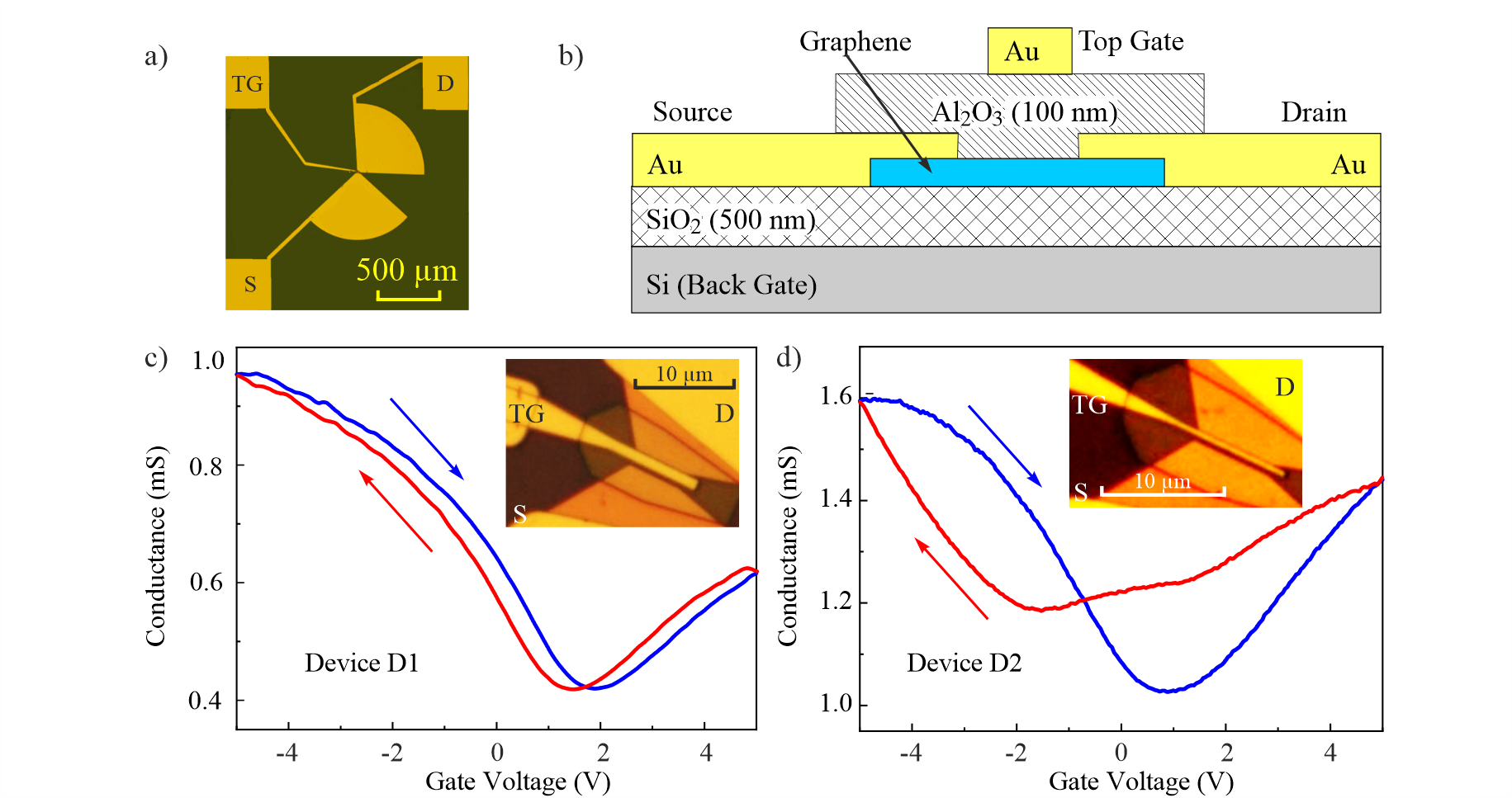
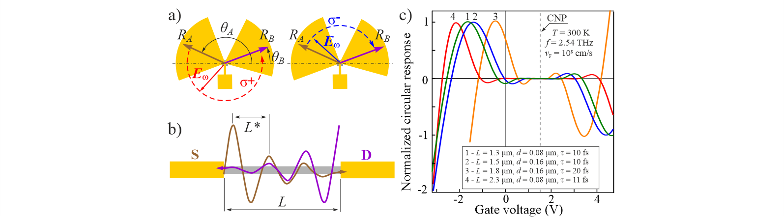
The single layer graphene (SLG), acting as the conducting channel of a field-effect transistor, was synthesized in a home-made cold-wall chemical vapor deposition reactor by chemical vapor deposition (CVD) on a copper foil with a thickness of 25 m Rybin2016 . SLG was transferred onto an oxidized silicon waferGayduchenko2018 , for more details see Appendix. The antenna sleeves were attached to the source and drain electrodes. To realize the helicity sensitive terahertz plasmonic interferometer, the antenna sleeves were bent by 45∘ as shown in Fig. 1b. The sleeves were made using photolithographic methods and metallization sputtering (Ti/Au, 5/100 nm). At the first lithography step, contact pads to graphene channel were formed using pure Au with a thickness of 25 nm. Note that we did not use adhesion sub layer (like titan or chrome) at this step. At the next technological step, e-beam evaporator was applied to sputter a 100 nm thick layer of Al2O3 that acts as a gate insulator. Note that Al2O3 layer reduces the initially high doping level of as-transferred graphene to almost zero Fallahazad2012 ; Kang2013 . Finally, the top gate electrode (Ti/Au, 5/200 nm) is patterned and formed using standard sputtering and lift-off techniques. The resulting structure is sketched in the Figure 1a. Two devices with channel lengths 2 m (device 1) and 1 m (device 2) were fabricated. Zoomed images of the channel parts are shown in insets in Figs. 1c and 1d. Note that for both devices the gates are deposited asymmetrically in respect to the channel. They cover about 75% (device 1) and 50% (device 2) of the channels and the gate stripes are located closer to the drain contact pads.
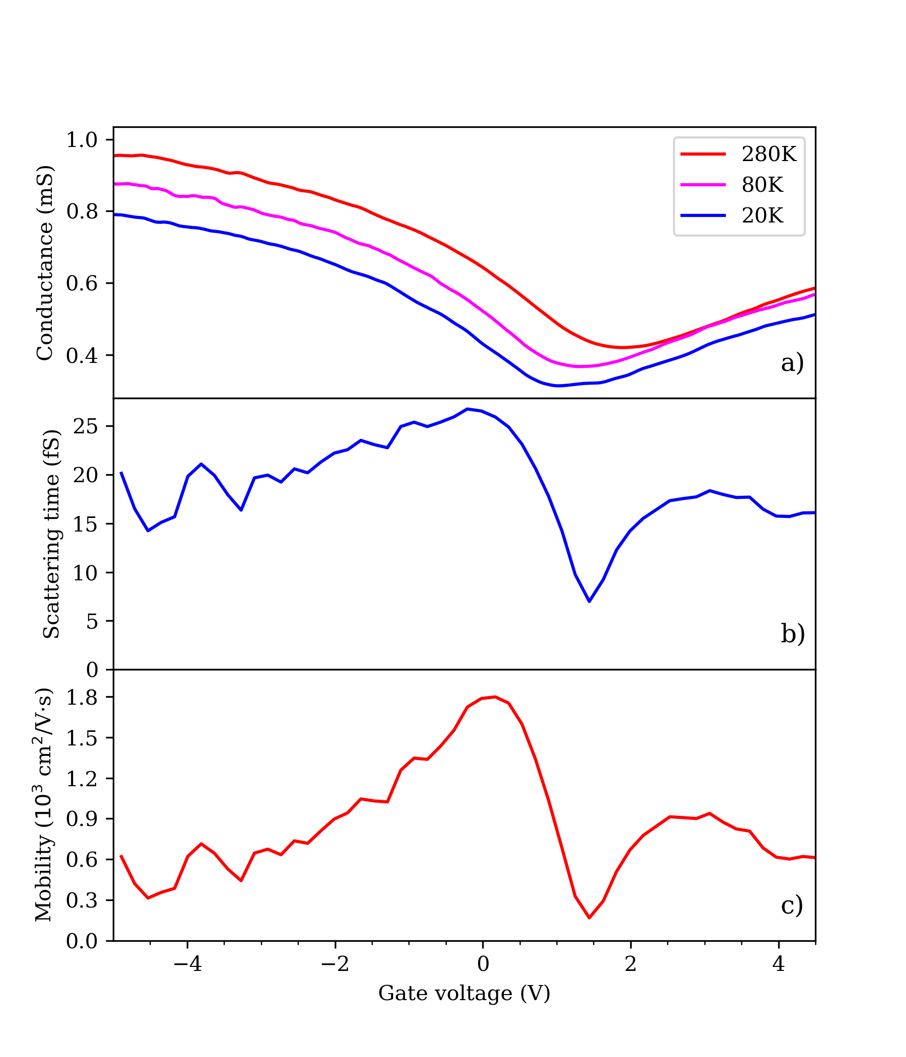
Typical transport characteristics of our graphene devices are shown in the Figs. 1c and 1d. For different directions of the gate voltage sweep as well as the sample cooldowns, the charge neutrality point (CNP) can occur at different gate voltages . This is well known feature and is possibly caused by the gate-sweep direction (cooldown-) dependent charge trapping. Therefore, below we indicate range of corresponding to the CNP instead of providing its exact value. Comparing conductance curves of the device 1 and 2 shows that the minimal conductance scales as an inverse of the graphene channel length, indicating that most of the resistance comes from the graphene channel itself rather than from the contacts. Analysis of the channel mobilities and corresponding scattering times is presented in Appendix. Using the Drude formula generalized for graphene we estimate scattering times of the order of 10-20 fs for, e.g., device 1 at room temperature. Finally, we note that the curves do not change as the temperature goes down (see Appendix), meaning that mobility is restricted by the defect scattering.
The experiments have been performed applying a continuous wave methanol laser operating at frequencies THz (wavelength m) with a power of mW and THz (wavelength m) with mW Ganichev2009 ; Kvon2008 . The laser spot with a diameter of about 1-3 mm is substantially larger than the sample size ensuring uniform illumination of both antennas. The radiation polarization state was controllably varied by means of lambda-half plate that rotates the polarization direction of linear polarized radiation and lambda-quarter plate that transforms linearly polarized radiation into elleptically polarized one.
The helicity of the radiation is then controlled via changing the angle between the laser polarization and the main axes of the lambda-quarter plate, so that for the radiation is right circularly polarized () and for - left circularly polarized (). The functional behavior of the Stokes parameters upon rotation of the waveplates is summarized in Appendix, see also Ref. [61]. The samples were placed in an temperature variable optical cryostat and photoresponse was measured as the voltage drop directly over the sample applying lock-in technique at a modulation frequency of 75 Hz.
III Results
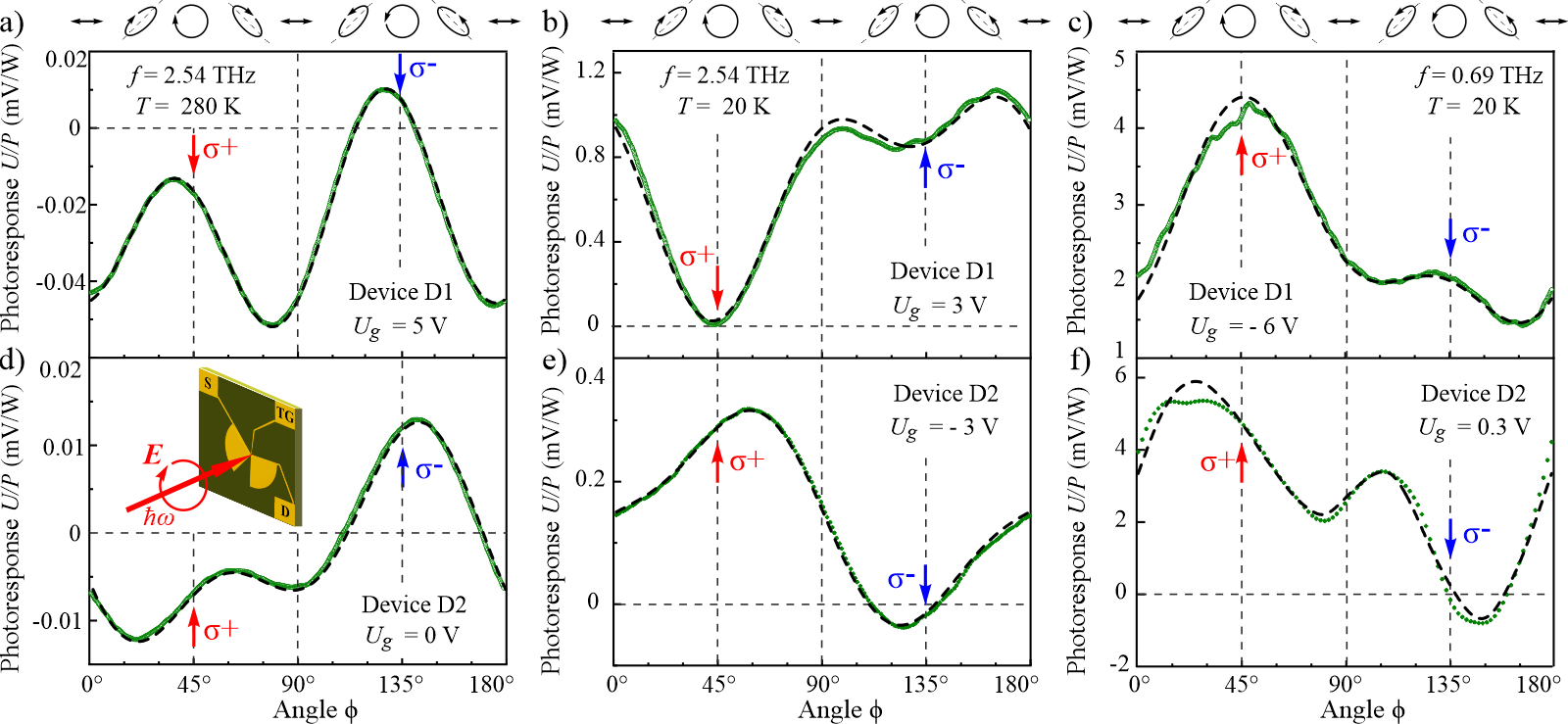
The principal observation made in our experiment is that for all investigated devices the response to a circularly polarized radiation crucially depends on its helicity. Fig. 2 displays the response voltage normalized by the radiation intensity as a function of the angle obtained under different conditions. We emphasize significant difference in the signal for and , corresponding to opposite helicities of circularly polarized light, in particular, the sign inversion observed under some conditions, see e.g. Fig. 2d. The effect is observed for radiation with frequencies 2.54 and 0.69 THz in a wide temperature range from 4.2 K to 300 K. The overall dependence of the signal on angle is more complex and is well described by
with , , and are fit parameters depending on gate voltage, temperature and radiation frequency. Note that trigonometric functions used for the fit are the radiation Stokes parameters describing the degree of the circular and linear polarization (see Appendix) bahaasaleh2019 ; Belkov2005 ; Weber2008 . While three last terms are insensitive to the radiation helicity the first term () is -periodic and describes helicity-sensitive response: it reverses the sign upon switching from right- () to left- () handed circular polarization. Figure 2 reveals that this term gives substantial contribution to the total signal. As we show below the -periodic term is related to the plasma interference in the graphene-based FET channel. Measurements at room and low temperatures demonstrate that cooling the device increases the amplitude of the circular photoresponse by more than ten times, see Figs. 2a and 2b as well as 2d and 2e. The signal increase is also observed by reduction of radiation frequency, see Figs. 2b and 2c as well as 2e and 2f.
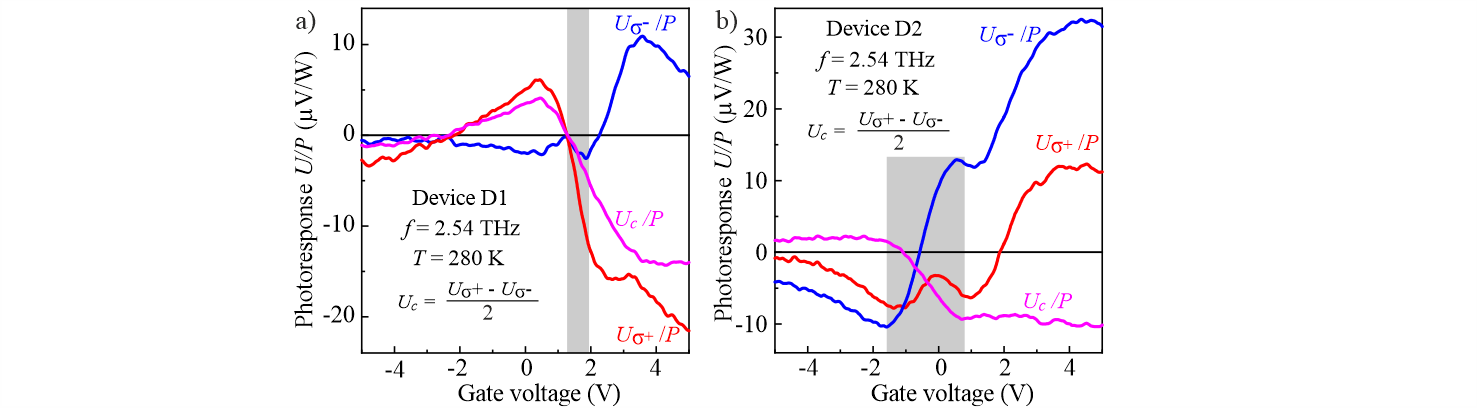
Having experimentally proved the applicability of Eq. (III) and substantial contribution of the helicity drive signal we now concentrate on the dependence of the parameter on the gate voltage that controls the type and concentration of the charge carriers in the FET channel. We use the following procedure: we obtain the gate voltage dependence of the response voltage normalized to the radiation power for two positions of the plate and , corresponding to opposite helicities of circularly polarized light ( and ). The half-difference between these two curves directly gives gate voltage dependence of the helicity sensitive photoresponse [see Eq. (III)] Results of these measurements, shown in Fig. 3, reveal that is more pronounced at positive gate voltage, where the channel is electrostatically doped with electrons, and changes the sign close to the CNP. As addressed above the variation of the CNP from measurement to measurement does not allow us to allocate the exact position of the CNP for the gate voltage sweeps during the photoresponse measurements. Note that for the device 1, having the gate length twice larger as that of device 2, at large negative gate voltages the second sign inversion of the photocurrent is present. Figure 3a indicates that in device 1 for the whole range of gate voltages photoresponse for - and - radiation have consistently opposite sign indicating negligible contribution of the polarization independent background. In device 2, however, the background is of the same order as the helicity sensitive response , see Fig. 3b.
Finally, we present additional data on the contributions proportional to fit parameters , and in Eq. (III). As discussed above these contributions do not connected to the radiation helicity and are related to the Stokes parameters describing the degrees of linear polarization (terms and ) and radiation intensity (term ). In experiments applying linearly polarized radiation with rotation of plates Stokes parameters modifies and polarization dependence Eq. (III) takes a form
| (2) |
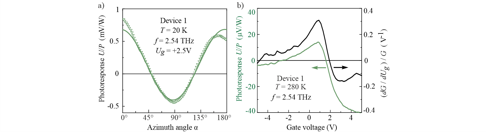
An example of the photoresponse variation upon change of the azimuth angle is shown in Fig. 4a. The data reflects the specific antenna pattern of our devices with tilted sleeves. Figure 4b shows the gate voltage dependence of the photoresponse obtained in device 1 for . Comparing these plots with the results for circular photoresponse shows that they behave similarly: in both cases signal changes the sign close to CNP and the response for positive gate voltages is larger than that for negative . Transport measurements carried out parallel to photoresponse measurements show that the photosignal behaves similarly to the normalized first derivative of the conductance over : , see Fig. 4a. Note that this behavior is well known for non-coherent, phase-insensitive plasmonic detectors Veksler2006 .
IV Theory and discussion
Conversion of THz radiation into dc voltage can be obtained due to several phenomena including photothermoelectric (PTE) effects Fedorov2013 ; Gabor2011 ; Fuhrer2014 , rectification on inhomogeneity of carrier doping in gated structures Fuhrer2014 ; Gayduchenko2018 ; CastillaKoppens2019 , photogalvanic and photon drag effects Karch2010 ; Jiang2011 ; Glazov2014 as well as rectification of electromagnetic waves in a FET channel supporting plasma waves Dyakonov1996 . However, in our experiment only plasmonic mechanism can yield the dc voltage whose polarity changes upon switching the radiation helicity. Indeed, PTE effects and rectification due to gradient of carrier doping in gated structures are based on inhomogeneities of either radiation heating or radiation absorption, which are helicity-insensitive b1 .
Below, we show that the helicity-sensitive plasmonic response originates from the interference of plasmonic signals excited by the source and drain antenna sleeves. The source and drain potentials with respect to the top gate are given by
| (3) |
where is the radiation frequency. Complex amplitudes and of the signal at source and drain, respectively, are proportional to the electric field amplitude of the incident electromagnetic wave. Their amplitudes and the phase shift between signals () depend on the radiation polarization and antennas geometry, see Appendix. Design of our devices, see Fig. 5a, ensures asymmetric coupling of radiation to the source and drain electrodes so that both amplitudes and phases of source and drain potentials are different. Most importantly, when such a bent bow-tie antenna is illuminated by circularly polarized radiation, the source- and drain-related antenna sleeves are polarized with a time delay because of rotation of the electric field vector. For circularly polarized wave, the phase shift changes sign with changing the helicity of the radiation: for (positive helicity) and for (negative helicity ), where and are geometrical angles of antennas sleeves. Equations describing more general case of elliptic polarization are derived in Appendix. We note that in the case of linear polarization, the phase shift is zero and the second term in Eq. (4) is absent.
Due to hydrodynamic non-linearity of plasma waves Dyakonov1993 ; Dyakonov1996 DC voltage across the channel appears
| (4) |
where and are gate-controlled coefficients which represent, respectively, non-coherentDyakonov1996 and interference Drexler2012 ; Romanov2013 ; gorbenko2018single ; Gorbenko2019 contributions to the response. This coefficients do not depend on signal phases and amplitudes, while all information about coupling with antennas is encoded in factors and .
For the case of radiation with arbitrary polarization characterized by the Stockes parameters, that are controlled by the orientation of the plate, defined by the phase angle , we obtain
| (5) | |||||
Here , , , are the geometrical factors calculated in Appendix for a simplified model. Note that these factors are independent of the gate voltage, so that the entire gate voltage dependence of the photoresponse is defined by the factors and . Comparing these results with empirical Eq. (III) we conclude that the data shown in the Fig. 2 are fully consistent with theoretical considerations discussed thus far. In particular, the interference-induced helicity-sensitive contribution, given by the last term on the right hand side of the above equation, is clearly observed in the experiment, see Fig. 2.
Such interference contribution appears when source and drain electrodes “talk” to each other via exchange of plasma wave phase-shifted excitations. Hence, the characteristic length of plasma wave decay should not be too small as compared to channel length so that plasmons excited near source and drain electrodes could efficiently interfere within the channel, see the Fig. 5b. As the gate voltage controls the type and concentration of the charge carriers it also controls the velocity of the plasma waves and the length As a result, the second term in the Eq. (4) should oscillate as function of the gate voltage. The general formulas for response given in Appendix can be essentially simplified for the non-resonant case , which corresponds to our experimental situation b2 . In this case, plasma waves decay from the source and drain part of the channel within the length and the response is given by Eq. (38) in Appendix. The parameters in Eq. (5) are given by
| (6) |
In our experiment was essentially smaller than the device length: . However, the interference, helicity-dependent part of the response was clearly seen in the experiment. The result of calculations are presented in Fig. 5c. For gate voltages far from the Dirac point we obtain a qualitative agreement of the calculations and results of experiments presented in Fig. 3a:
-
•
the circular photoresponse at high positive gate voltages and for moderate negative have opposite sign;
-
•
with increase of the negative gate voltages value the response changes its sign;
-
•
in the vicinity of the Dirac point calculations yield oscillations of the circular response.
The last statement needs a clarification. While the oscillations are not visible in the experimental magenta curve of Fig. 3a, showing , in individual curves obtained for left- (blue curve) and right- (red curve) they are clearly present. This difference is caused by the fact that the and curves represent the results of two different experiments, namely, measurements for and radiation. At the same time, is obtained as a result of subtraction of these two curves, corresponding to different sweeps. Due to the hysteresis of the discussed above in Sec. 2, the sample parameters were slightly different for these two measurements. As a result, the oscillations present in one curve are superimposed with larger featureless signal from the other. Furthermore, Fig. 3b shows that presence of the oscillations in photoresponse to circularly polarized radiation for the second device too.
Now we estimate the period of the oscillations. The dependence on the gate voltage is mostly encoded in The oscillations period can be estimated from the condition which gives For V and we find V in a good agreement with experiment. We also note that the experimentally observed oscillations (see blue curve for the device 1) decays at the same scale as an oscillation period in an excellent agreement with behavior of the function , see Eq. (6).
Finally, we emphasize that the presence of oscillations in the hallmark of the interference part of response. Importantly, the response to the linearly polarized radiation does not show any oscillations in the vicinity of the CNP, see Fig. 4b. By contrast it just follows to — a well know behavior for Dyakonov-Shur non-coherent plasmonic detectors, see e.g. Ref. [50]. Note that for linearly polarized radiation the above theory also yields this gate dependence, see structureless expression for non-coherent contribution in Eq. (6).
V Summary
To summarize, we demonstrated that specially designed graphene-based FET can be used to study plasma wave interference effects. Our approaches can be extrapolated to other 2D materials and used as a tool to characterize optically-induced plasmonic excitations. Specifically, the conversion of the interfering plasma waves into dc response is controlled by the gate voltage and encodes information about helicity of the radiation and phase difference between the plasmonic signals. Remarkably, our work shows that CVD graphene with moderate mobility, which is compatible with most standard technological routes can be used as a material for active plasmonic devices. The suggested device design can be used for a broad-band helicity-sensitive interferometer capable of analyzing both polarization of THz radiation and geometrical phase shift caused by antennas asymmetry. By the proper choice of the antenna design and FET parameters, phase-sensitive and fast room temperature plasmonic detectors can be tuned to detect individual Stokes parameters. Hence, our work paves a novel way for developing the all-electric detectors of the terahertz radiation polarization state.
VI Acknowledgements
The work was supported by the FLAG-ERA program (project DeMeGRaS, project GA501/16-1 of the DFG), the Russian Foundation for Basic Research within Grants No. 18-37-20058 and No. 18-29-20116, the Volkswagen Stiftung Program (97738) and Foundation for Polish Science (IRA Program, grant MAB/2018/9, CENTERA). The work of V.K. was supported by the Russian Science Foundation (Grant No. 20-12-00147). The work of I.G. was supported by Russian Foundation for Basic Research (Grant No. 20-02-00490) and by Foundation for the Advancement of Theoretical Physics and Mathematics BASIS. M.M. acknowledges support of Russian Science Foundation (project No. 17-72-30036) in sample design.
VII Appendix
VII.1 Devices, experimental details and fit parameters
Device fabrication. The single layer graphene (SLG), acting as the conducting channel of a field-effect transistor, was synthesized in a home-made cold-wall chemical vapor deposition reactor by chemical vapor deposition (CVD) on a copper foil with a thickness of 25 m Rybin2016 . SLG was transferred onto an oxidized silicon waferGayduchenko2018 . The silicon substrate consists of 480 m thick silicon wafer covered with a 500 nm thick thermally grown SiO2 layer. Note that silicon used for the substrate (with the room temperature resistivity of 10 cm) is transparent for the sub-THz and THz radiation. After transferring graphene onto a silicon wafer the geometry of the device is further defined by e-beam lithography using a PMMA mask and oxygen plasma etching.
At the first lithography step, contact pads to graphene channel were formed using pure Au with a thickness of 25 nm. Note that we did not use adhesion sub layer (like titan or chrome) at this step. At the next technological step, e-beam evaporator was applied to sputter a 100 nm thick layer of Al2O3 that acts as a gate insulator. Note that Al2O3 layer reduces the initially high doping level of as-transferred graphene to almost zero Fallahazad2012 ; Kang2013 .
Afterward, the antenna sleeves were attached to the source and drain electrodes. To realize the helicity sensitive terahertz plasmonic interferometer, the antenna sleeves were bent by 45∘ as shown in Fig. 1a. The sleeves were made using photolithographic methods and metallization sputtering (Ti/Au, 5/100 nm). Finally, the top gate electrode (Ti/Au, 5/200 nm) is patterned and formed using standard sputtering and lift-off techniques. The resulting structure is sketched in Fig. 1b of the main text. Two devices with channel lengths 2 m (device 1) and 1 m (device 2) were fabricated. Zoomed images of the channel parts are shown in insets in Figs. 1c and d of the main text. Note that for both devices the gates are deposited asymmetrically in respect to the channel. They cover about 75% (device 1) and 50% (device 2) of the channels and the gate stripes are located closer to the drain contact pads.
Transport characteristics and transport scattering time. Typical transport characteristics of our graphene devices are shown in the Figs. 1c and 1d of the main text. For different directions of the gate voltage scan as well as the sample cooldowns, the charge neutrality point (CNP) can occur at different gate voltages. This is well known feature and is possibly caused by the gate-scan-direction (cooldown-) dependent charge trapping. Therefore, below we indicate range of corresponding to the CNP instead of providing its exact value. Comparing conductance curves of the device 1 and 2 shows that the minimal conductance scales as an inverse of the graphene channel length, indicating that most of the resistance comes from the graphene channel itself rather than from the contacts. For that we used the transfer curves measured in two-probe configuration, since we cannot perform four contacts Hall effect measurements due to configuration of our devices.
We extract mobility and transport scattering time from the conductance measurements shown in Fig. 6a. The conductivity of graphene is given by
| (7) |
where is the Fermi energy and is the energy-dependent transport scattering time. The Fermi energy depends on the concentration, which is controlled by the gate voltage: where is the gate voltage counted from the Dirac point, is the dielectric constant and is the width of the spacer. Here, in all calculations, we assume that having in mind that response should change sign under replacement Using Eq. (7) and the formula
| (8) |
one can extract from experimental data (see Fig. 6a) the dependence of both and mobility, defined as
| (9) |
on The result is presented in Figs. 6b and c. Assuming that with approaching to the neutrality point the scattering is limited by charged impurities, for which
| (10) |
we approximate the experimental dependence shown in Fig. 6b as
| (11) |
where s and Equation (11) was used to calculate and entering Eq. (34). We also used the well known expression for plasma wave velocity in graphene
| (12) |
Equations (11) and (12) become invalid very close to the neutrality point. Finally, we note that the curves do not change as the temperature goes down, meaning that mobility is restricted by the defect scattering.
Laser and experimental setup. The experiments have been performed applying a continuous wave (CW) methanol laser operating at frequencies THz (wavelength m) with a power of mW and THz (wavelength m) with mW Ganichev2009 ; Kvon2008 . The incident radiation power was monitored by a reference pyroelectric detector. The laser beam was focused onto the sample by a parabolic mirror with a focal length of 75 mm. Typical laser spot diameters varied, depending on the wavelength, from 1 to 3 mm. The spatial laser beam distribution had an almost Gaussian profile, checked with a pyroelectric camera Ziemann2000 . The radiation was modulated at about 75 Hz by an optical chopper. The samples were placed in an optical temperature variable cryostat and photoresponse was measured as a voltage drop using standard lock-in technique. The radiation of the laser was linearly polarized. To demonstrate sensitivity of the photovoltage to the helicity of the incoming radiation we place a plate made of -cut crystalline quartz in the incoming beam. The helicity of the radiation is then controlled via changing the angle between the laser polarization and the main axes (“fast direction”) rotating the plate in vertical plane. When the radiation incident on the device is clock wise circularly polarized (right circularly polarized radiation, ) while for one gets the opposite polarization (left circularly polarized radiation, ). To study response to the linearly polarized radiation we used -plates. Rotating the plate, we rotated the radiation electric field vector by an azimuth angle .
Fitting parameters. The curves in Fig. 2 were obtained with fitting parameters summarized in Tab. 1.
| Panel in Fig. 2 | a) | b) | c) | d) | e) | f) |
|---|---|---|---|---|---|---|
| -0.012 | -0.42 | 1.15 | 0.009 | 0.15 | 2.15 | |
| 0.025 | -0.14 | -0.08 | -0.007 | -0.09 | 3.34 | |
| -0.039 | 0.49 | -1.03 | -0.009 | 0.01 | 0.52 | |
| -0.005 | 0.46 | 3.18 | 0.003 | 0.13 | 2.58 |
VII.2 Response to polarization of arbitrary polarization
We assume that wavelength of the radiation is much larger that the device size and that incoming beam linearly polarized along axis acquires elliptical polarization after transmission through plate. Then, the field is described by homogeneous electric vector with the components
| (13) | |||||
| (14) |
where
| (15) |
We get
| (16) | |||||
| (17) | |||||
| (18) | |||||
| (19) |
Here, we introduced Stokes parameters
| (20) | |||||
| (21) | |||||
| (22) |
where is the rotation angle of plate with respect to axis. As seen, the angles correspond to linear polarization along axis, while angles (or ) and (or ) to circular polarization with right and left helicity, respectively. We note that the helicity also changes sign by inversion of the radiation frequency: For definiteness, in all equations below we assume
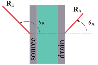
The detailed analysis of time-dependent potential distribution in our device requires calculation of antennas properties, which is a challenging problem beyond the scope of the current work. However, some phenomenological properties of suggested interferometer can be understood by using a toy model, which captures basic physics of the problem. The model is illustrated in Fig. 7, where two antennas are replaced with long thin metallic rods described by vectors . Assuming that antennas are perfect conductors and neglecting small mutual capacitances, one can write the potentials applied to source and drain as
where parameters and for obey [see Eqs. (13) and (14)]
| (23) | |||
| (24) |
In the simplest case of circular polarization considered in Refs. S1 ; S2 (), equations (23) and (24) simplifies, so that and for (positive helicity) and for (negative helicity). For the case of generic elliptic polarization, it is convenient to use the Stokes parameters. After simple algebra, we find equations needed for calculation of the response according to the theory developed in Refs. S1 ; S2
| (25) |
| (26) |
where
| (27) | |||||
| (28) | |||||
| (29) | |||||
| (30) |
are purely geometrical factors. Although these factors can change for a more realistic models of antennas, the general structure of Eqs. 25 and 26 should remain the same, so that one can use and as fitting parameters that do not depend on frequency and gate voltage. Importantly, terms proportional to and to have different angle periodicity— and respectively—that allows one to separate them in experiment. Dependence of the response on can be found by using results of Ref. S1 [see Eqs. (14-16) in S1 ] :
| (31) |
| (32) |
where is the plasma wave velocity, is the length of the FET channel,
| (33) |
is the plasma wave vector, is the inverse momentum relaxaton time, and and are effective frequency and damping rate of the plasma waves, given by
| (34) |
and the coefficients and read
| (35) | |||
| (36) |
Equation (32) can be written in form of Eq. (5) with
| (37) | |||
| (38) |
The coefficients and entering Eq. (III) reads
| (39) |
VII.3 Interference part of the response
Eq. (32) allows to extract experimentally interference contribution to response. We find
| (40) |
Hence, interference term in our setup depends only on circular component of polarization. Using simplified formula for geometrical factor, [see Eq. (30)], we rewrite Eq. (40) as follows
| (41) |
We see that the response is proportional to One can show that for device with a beam splitter and a delay line one should simply add in Eq. (41) the delay line phase shift to geometrical phase shift :
| (42) |
VII.4 Non-resonant regime
Equations (34), (35), (36), (37) and (38) simplify in the non-resonant regime, under additional assumption (long non-resonant sample S1 ). Here
| (43) |
is the plasma wave decay length. In this regime, plasma waves, excited at the source and drain parts of the channel weakly overlap inside the transistor channel. The response becomes S1 ; b3
| (44) |
while the coefficients and are given by Eqs. (6) of the main text. Physically, last phase- and helicity-sensitive term in Eq. (44) describes interference arising due to overlapping of the plasma waves.
References
- (1) M. O. Scully and M. S. Zubairy, Quantum Optics (Cambridge University Press, 1997), URL https://doi.org/10.1017/cbo9780511813993.
- (2) Basics of Interferometry (Elsevier, 2007), URL https://doi.org/10.1016/b978-0-12-373589-8.x5000-7.
- (3) R. Demkowicz-Dobrzański, M. Jarzyna, and J. Kołodyński, in Progress in Optics (Elsevier, 2015), pp. 345435, URL https://doi.org/10.1016/bs.po.2015.02.003.
- (4) J.-W. Pan, Z.-B. Chen, C.-Y. Lu, H. Weinfurter, A. Zeilinger, and M. Żukowski, Rev. Mod. Phys. 84, 777 (2012), URL https://doi.org/10.1103/revmodphys.84.777.
- (5) S. Ganichev, S. Yemelyanov, E. Ivchenko, E. Perlin, Y. Terent’ev, A. Fedorov, and I. Yaroshetskii, J. Exp. Theor. Phys. 64, 729 (1986).
- (6) B. J. Keay, S. J. Allen, J. Galán, J. P. Kaminski, K. L. Campman, A. C. Gossard, U. Bhattacharya, and M. J. W. Rodwell, Phys. Rev. Lett. 75, 4098 (1995), URL https://doi.org/10.1103/physrevlett.75.4098.
- (7) D. H. Boal, C.-K. Gelbke, and B. K. Jennings, Rev. Mod. Phys. 62, 553 (1990), URL https://doi.org/10.1103/revmodphys.62.553.
- (8) A. D. Cronin, J. Schmiedmayer, and D. E. Pritchard, Rev. Mod. Phys. 81, 1051 (2009), URL https://doi.org/10.1103/revmodphys.81.1051.
- (9) A. J. Uzan, H. Soifer, O. Pedatzur, A. Clergerie, S. Larroque, B. D. Bruner, B. Pons, M. Ivanov, O. Smirnova, and N. Dudovich, Nat. Photonics 14, 188 (2020), URL https://doi.org/10.1038/s41566-019-0584-2.
- (10) D. Becker, M. D. Lachmann, S. T. Seidel, H. Ahlers, A. N. Dinkelaker, J. Grosse, O. Hellmig, H. M’́untinga, V. Schkolnik, T. Wendrich, et al., Nature 562, 391 (2018), URL https://doi.org/10.1038/s41586-018-0605-1.
- (11) A. Danner, B. Demirel, W. Kersten, H. Lemmel, R. Wagner, S. Sponar, and Y. Hasegawa, Npj Quantum Inf. 6, 23 (2020), URL https://doi.org/10.1038/s41534-020-0254-8.
- (12) B. Yin, Z. Piao, K. Nishimiya, C. Hyun, J. A. Gardecki, A. Mauskapf, F. A. Jaffer, and G. J. Tearney, Light: Sci. Appl. 8, 104 (2019), URL https://doi.org/10.1038/s41377-019-0211-5.
- (13) H. Spahr, C. Pf’́ affe, S. Burhan, L. Kutzner, F. Hilge, G. H’́uttmann, and D. Hillmann, Sci. Rep. 9, 11748 (2019), URL https://doi.org/10.1038/s41598-019-47979-8.
- (14) S. Shevchenko, S. Ashhab, and F. Nori, Phys. Rep. 492, 1 (2010), URL https://doi.org/10.1016/j.physrep.2010.03.002.
- (15) Z. Wang, W.-C. Huang, Q.-F. Liang, and X. Hu, Sci. Rep. 8, 7920 (2018), URL https://doi.org/10.1038/s41598-018-26324-5.
- (16) S. K. Saha, Rev. Mod. Phys. 74, 551 (2002), URL https://doi.org/10.1103/revmodphys.74.551.
- (17) K. Goda, O. Miyakawa, E. E. Mikhailov, S. Saraf, R. Adhikari, K. McKenzie, R. Ward, S. Vass, A. J. Weinstein, and N. Mavalvala, Nat. Phys. 4, 472 (2008), URL https://doi.org/10.1038/nphys920.
- (18) R. X. Adhikari, Rev. Mod. Phys. 86, 121 (2014), URL https://doi.org/10.1103/revmodphys.86.121.
- (19) S. Sala, A. Ariga, A. Ereditato, R. Ferragut, M. Giammarchi, M. Leone, C. Pistillo, and P. Scampoli, Sci. Adv. 5, eaav7610 (2019), URL https://doi.org/10.1126/sciadv.aav7610.
- (20) D. K. Gramotnev and S. I. Bozhevolnyi, Nat. Photonics 4, 83 (2010), URL https://doi.org/10.1038/nphoton.2009.282.
- (21) O. Graydon, Nat. Photonics 6, 139 (2012), URL https://doi.org/10.1038/nphoton.2012.45.
- (22) J. Ali, N. Pornsuwancharoen, P. Youplao, M. Aziz, S. Chiangga, J. Jaglan, I. Amiri, and P. Yupapin, Results Phys. 8, 438 (2018), URL https://doi.org/10.1016/j.rinp.2017.12.055.
- (23) Z. Khajemiri, S. Hamidi, and O. K. Suwal, Opt. Commun. 427, 85 (2018), URL https://doi.org/10.1016/j.optcom.2018.06.032.
- (24) Z. Khajemiri, D. Lee, S. M. Hamidi, and D.-S. Kim, Sci. Rep. 9, 1378 (2019), URL https://doi.org/10.1038/s41598-018-37499-2.
- (25) Z. Zhang, Y. Chen, H. Liu, H. Bae, D. A. Olson, A. K. Gupta, and M. Yu, Opt. Express 23, 10732 (2015), URL https://doi.org/10.1364/oe.23.010732.
- (26) Y. Salamin, I.-C. Benea-Chelmus, Y. Fedoryshyn, W. Heni, D. L. Elder, L. R. Dalton, J. Faist, and J. Leuthold, Nat. Commun. 10, 5550 (2019), URL https://doi.org/10.1038/s41467-019-13490-x.
- (27) G. Yuan, E. T. F. Rogers, and N. I. Zheludev, Light:Sci. Appl. 8, 2 (2019), URL https://doi.org/10.1038/s41377-018-0112-z.
- (28) A. Woessner, Y. Gao, I. Torre, M. B. Lundeberg, C. Tan, K. Watanabe, T. Taniguchi, R. Hillenbrand, J. Hone, M. Polini, et al., Nat. Photonics 11, 421 (2017), URL https://doi.org/10.1038/nphoton.2017.98.
- (29) A. Smolyaninov, A. E. Amili, F. Vallini, S. Pappert, and Y. Fainman, Nat. Photonics 13, 431 (2019), URL https://doi.org/10.1038/s41566-019-0360-3.
- (30) T. K. Hakala, A. J. Moilanen, A. I. V’́akev’́ainen, R. Guo, J.-P. Martikainen, K. S. Daskalakis, H. T. Rekola, A. Julku, and P. T’́orm’́a, Nat. Phys. 14, 739 (2018), URL https://doi.org/10.1038/s41567-018-0109-9.
- (31) B. S. Dennis, M. I. Haftel, D. A. Czaplewski, D. Lopez, G. Blumberg, and V. A. Aksyuk, Nat. Photonics 9, 267 (2015), URL https://doi.org/10.1038/nphoton.2015.40.
- (32) C. Haffner, W. Heni, Y. Fedoryshyn, J. Niegemann, A. Melikyan, D. L. Elder, B. Baeuerle, Y. Salamin, A. Josten, U. Koch, et al., Nat. Photonics 9, 525 (2015), URL https://doi.org/10.1038/nphoton.2015.127.
- (33) D. Mittleman, Sensing with Terahertz Radiation (Springer Series in Optical Sciences, 2010).
- (34) S. S. Dhillon, M. S. Vitiello, E. H. Lineld, A. G. Davies, M. C. Hoffmann, J. Booske, C. Paoloni, M. Gensch, P. Weightman, G. P. Williams, et al., J. Phys. D:Appl. Phys. 50, 043001 (2017), URL https://doi.org/10.1088/1361-6463/50/4/043001.
- (35) C. Drexler, N. Dyakonova, P. Olbrich, J. Karch, M. Schafberger, K. Karpierz, Y. Mityagin, M. B. Lifshits, F. Teppe, O. Klimenko, et al., J. Appl. Phys. 111, 124504 (2012), URL https://doi.org/10.1063/1.4729043.
- (36) K. S. Romanov and M. I. Dyakonov, Appl. Phys. Lett. 102, 153502 (2013), URL https://doi.org/10.1063/1.4801946.
- (37) I. Gorbenko, V. Kachorovskii, and M. Shur (2018), 1810.06429.
- (38) I. V. Gorbenko, V. Y. Kachorovskii, and M. Shur, Opt. Express 27, 4004 (2019), URL https://doi.org/10.1364/oe.27.004004.
- (39) M. Dyakonov and M. Shur, Phys. Rev. Lett. 71, 2465 (1993), URL https://doi.org/10.1103/physrevlett.71.2465.
- (40) M. Dyakonov and M. Shur, IEEE Trans. Electron Devices 43, 380 (1996), URL https://doi.org/10.1109/16.485650.
- (41) W. Knap, M. Dyakonov, D. Coquillat, F. Teppe, N. Dyakonova, J. Lusakowski, K. Karpierz, M. Sakowicz, G. Valusis, D. Seliuta, et al., J. Infrared Millim. Terahertz Waves 30, 1319 (2009), URL https://doi.org/10.1007/s10762-009-9564-9.
- (42) R. Tauk, F. Teppe, S. Boubanga, D. Coquillat, W. Knap, Y. M. Meziani, C. Gallon, F. Boeuf, T. Skotnicki, C. Fenouillet-Beranger, et al., Appl. Phys. Lett. 89, 253511 (2006), URL https://doi.org/10.1063/1.2410215.
- (43) M. Sakowicz, J. Łusakowski, K. Karpierz, M. Grynberg, W. Knap, K. K’́ohler, G. Valušis, K. Gołaszewska, E. Kamińska, and A. Piotrowska, Appl. Phys. Lett. 92, 203509 (2008), URL https://doi.org/10.1063/1.2930682.
- (44) W. Knap, V. Kachorovskii, Y. Deng, S. Rumyantsev, J.-Q. Lu, R. Gaska, M. S. Shur, G. Simin, X. Hu, M. A. Khan, et al., J. Appl. Phys. 91, 9346 (2002), URL https://doi.org/10.1063/1.1468257.
- (45) W. Knap, Y. Deng, S. Rumyantsev, and M. S. Shur, Appl. Phys. Lett. 81, 4637 (2002), URL https://doi.org/10.1063/1.1525851.
- (46) X. G. Peralta, S. J. Allen, M. C. Wanke, N. E. Harff, J. A. Simmons, M. P. Lilly, J. L. Reno, P. J. Burke, and J. P. Eisenstein, Appl. Phys. Lett. 81, 1627 (2002), URL https://doi.org/10.1063/1.1497433.
- (47) T. Otsuji, M. Hanabe, and O. Ogawara, 85, 2119 (2004), URL https://doi.org/10.1063/1.1792377.
- (48) F. Teppe, W. Knap, D. Veksler, M. S. Shur, A. P. Dmitriev, V. Y. Kachorovskii, and S. Rumyantsev, Appl. Phys. Lett. 87, 052107 (2005), URL https://doi.org/10.1063/1. 2005394.
- (49) F. Teppe, D. Veksler, V. Y. Kachorovski, A. P. Dmitriev, X. Xie, X.-C. Zhang, S. Rumyantsev, W. Knap, and M. S. Shur, Appl. Phys. Lett. 87, 022102 (2005), URL https://doi.org/10.1063/1.1952578.
- (50) D. Veksler, F. Teppe, A. P. Dmitriev, V. Y. Kachorovskii, W. Knap, and M. S. Shur, Phys. Rev. B: Condens. Matter Mater. Phys. 73, 125328 (2006), URL https://doi.org/10.1103/physrevb.73.125328.
- (51) D. Derkacs, S. H. Lim, P. Matheu, W. Mar, and E. T. Yu, Appl. Phys. Lett. 89, 093103 (2006), URL https://doi.org/10.1063/1.2336629.
- (52) A. E. Fatimy, S. B. Tombet, F. Teppe, W. Knap, D. Veksler, S. Rumyantsev, M. Shur, N. Pala, R. Gaska, Q. Fareed, et al., Electron. Lett 42, 1342 (2006), URL https://doi.org/10.1049/el:20062452.
- (53) L. Vicarelli, M. S. Vitiello, D. Coquillat, A. Lombardo, A. C. Ferrari, W. Knap, M. Polini, V. Pellegrini, and A. Tredicucci, Nat. Mater. 11, 865 (2012), URL https://doi.org/10.1038/nmat3417.
- (54) F. H. L. Koppens, T. Mueller, P. Avouris, A. C. Ferrari, M. S. Vitiello, and M. Polini, Nat. Nanotechnol. 9, 780 (2014), URL https://doi.org/10.1038/nnano.2014.215.
- (55) M. Rybin, A. Pereyaslavtsev, T. Vasilieva, V. Myasnikov, I. Sokolov, A. Pavlova, E. Obraztsova, A. Khomich, V. Ralchenko, and E. Obraztsova, Carbon 96, 196 (2016), URL https://doi.org/10.1016/j.carbon.2015.09.056.
- (56) I. A. Gayduchenko, G. E. Fedorov, M. V. Moskotin, D. I. Yagodkin, S. V. Seliverstov, G. N. Goltsman, A. Y. Kuntsevich, M. G. Rybin, E. D. Obraztsova, V. G. Leiman, et al., Nanotechnology 29, 245204 (2018), URL https://doi.org/10.1088/1361-6528/aab7a5.
- (57) B. Fallahazad, K. Lee, G. Lian, S. Kim, C. M. Corbet, D. A. Ferrer, L. Colombo, and E. Tutuc, Appl. Phys. Lett. 100, 093112 (2012), URL https://doi.org/10.1063/1.3689785.
- (58) C. G. Kang, Y. G. Lee, S. K. Lee, E. Park, C. Cho, S. K. Lim, H. J. Hwang, and B. H. Lee, Carbon 53, 182 (2013), URL https://doi.org/10.1016/j.carbon.2012.10.046.
- (59) S. D. Ganichev, S. A. Tarasenko, V. V. Bel’kov, P. Olbrich, W. Eder, D. R. Yakovlev, V. Kolkovsky, W. Zaleszczyk, G. Karczewski, T. Wojtowicz, et al., Phys. Rev. Lett. 102, 156602 (2009), URL https://doi.org/10.1103/physrevlett.102.156602.
- (60) Z.-D. Kvon, S. N. Danilov, N. N. Mikhailov, S. A. Dvoretsky, W. Prettl, and S. D. Ganichev, Physica E Low Dimens. Syst. Nanostruct. 40, 1885 (2008), URL https://doi.org/10.1016/j.physe.2007.08.115.
- (61) V. V. Bel’kov, S. D. Ganichev, E. L. Ivchenko, S. A. Tarasenko, W. Weber, S. Giglberger, M. Olteanu, H.-P. Tranitz, S. N. Danilov, P. Schneider, et al., J. Phys.: Condens. Matter 17, 3405 (2005), URL https://doi.org/10.1088/0953-8984/17/21/032.
- (62) B. E. A. Saleh, Fundamentals of Photonics, 2 Volume Set (Wiley Series in Pure and Applied Optics) (Wiley, 2019), ISBN 1119506875, URL https://www.xarg.org/ref/a/1119506875/.
- (63) W. Weber, L. E. Golub, S. N. Danilov, J. Karch, C. Reitmaier, B. Wittmann, V. V. Bel’kov, E. L. Ivchenko, Z. D. Kvon, N. Q. Vinh, et al., Phys. Rev. B: Condens. Matter Mater. Phys. 77, 245304 (2008), URL https://doi.org/10.1103/physrevb.77.245304.
- (64) G. Fedorov, A. Kardakova, I. Gayduchenko, I. Charayev, B. M. Voronov, M. Finkel, T. M. Klapwijk, S. Morozov, M. Presniakov, I. Bobrinetskiy, et al., Appl. Phys. Lett. 103, 181121 (2013), URL https://doi.org/10.1063/1.4828555.
- (65) N. M. Gabor, J. C. W. Song, Q. Ma, N. L. Nair, T. Taychatanapat, K. Watanabe, T. Taniguchi, L. S. Levitov, and P. Jarillo-Herrero, Science 334, 648 (2011), URL https://doi.org/10.1126/science.1211384.
- (66) X. Cai, A. B. Sushkov, R. J. Suess, M. M. Jadidi, G. S. Jenkins, L. O. Nyakiti, R. L. Myers-Ward, S. Li, J. Yan, D. K. Gaskill, et al., Nat. Nanotechnol. 9, 814 (2014), URL https://doi.org/10.1038/nnano.2014.182.
- (67) S. Castilla, B. Terrés, M. Autore, L. Viti, J. Li, A. Y. Nikitin, I. Vangelidis, K. Watanabe, T. Taniguchi, E. Lidorikis, et al., Nano Lett. 19, 2765 (2019), URL https://doi.org/10.1021/acs.nanolett.8b04171.
- (68) J. Karch, P. Olbrich, M. Schmalzbauer, C. Zoth, C. Brinsteiner, M. Fehrenbacher, U. Wurstbauer, M. M. Glazov, S. A. Tarasenko, E. L. Ivchenko, et al., Phys. Rev. Lett. 105, 227402 (2010), URL https://doi.org/10.1103/physrevlett.105.227402.
- (69) C. Jiang, V. A. Shalygin, V. Y. Panevin, S. N. Danilov, M. M. Glazov, R. Yakimova, S. Lara-Avila, S. Kubatkin, and S. D. Ganichev, Phys. Rev. B: Condens. Matter Mater. Phys. 84, 125429 (2011), URL https://doi.org/10.1103/physrevb.84.125429.
- (70) M. Glazov and S. Ganichev, Phys. Rep. 535, 101 (2014), URL https://doi.org/10.1016/j.physrep.2013.10.003.
- (71) While the circular photocurrents due to the photon drag and photogalvanic effects in the bulk of graphene have been observed previously (see the Ref. [70] for review), for present experimental geometry applying normal incident radiation, it is forbidden by symmetry arguments. This is because, for graphene with structure inversion asymmetry (induced by substrate and/or gate) described by C6v point symmetry, the circular photocurrents are allowed and experimentally demonstrated for oblique incidence onlyKarch2010 ; Jiang2011 ; Glazov2014 .
- (72) From the experimental conductance curves the scattering rate is estimated to be about 50 THz, which is much larger than the radiation frequency 2.54 THz used in our work.
- (73) E. Ziemann, S. D. Ganichev, W. Prettl, I. N. Yassievich, and V. I. Perel, J. Appl. Phys. 87, 3843 (2000), URL https://doi.org/10.1063/1.372423.
- (74) I. V. Gorbenko, V. Y. Kachorovskii, and M. S. Shur, physica status solidi (RRL) Rapid Research Letters p. 1800464 (2018), URL https://doi.org/10.1002/pssr.201800464.
- (75) I. V. Gorbenko, V. Y. Kachorovskii, and M. Shur, Optics Express 27, 4004 (2019), URL https://doi.org/10.1364/oe.27.004004.
- (76) In Ref. [74] Eq. (17) for non-resonant response of long sample contains typo. Correct equation is given by Eq. (24) of the arXive version of Ref. [74]: I. V. Gorbenko, V. Yu. Kachorovskii, M. S. Shur, arXiv:1807.05456