Assessing the defect tolerance of kesterite-inspired solar absorbers
Abstract
Various thin-film I2-II-IV-VI4 photovoltaic absorbers derived from kesterite Cu2ZnSn(S,Se)4 have been synthesized, characterized, and theoretically investigated in the past few years. The availability of this homogeneous materials dataset is an opportunity to examine trends in their defect properties and identify criteria to find new defect-tolerant materials in this vast chemical space. We find that substitutions on the Zn site lead to a smooth decrease in band tailing as the ionic radius of the substituting cation increases. Unfortunately, this substitution strategy does not ensure the suppression of deeper defects and non-radiative recombination. Trends across the full dataset suggest that Gaussian and Urbach band tails in kesterite-inspired semiconductors are two separate phenomena caused by two different antisite defect types. Deep Urbach tails are correlated with the calculated band gap narrowing caused by the (2III+IVII) defect cluster. Shallow Gaussian tails are correlated with the energy difference between the kesterite and stannite polymorphs, which points to the role of (III+III) defect clusters involving Group IB and Group IIB atoms swapping across different cation planes. This finding can explain why in-plane cation disorder and band tailing are uncorrelated in kesterites. Our results provide quantitative criteria for discovering new kesterite-inspired photovoltaic materials with low band tailing.
I Introduction
Progress in the photovoltaic efficiency of kesterite Cu2ZnSn(S,Se)4 solar cells has been minimal after reaching the 12.6% efficiency mark in 2013. Giraldo et al. (2019) While interface-related issues may be solved by an appropriate choice of contact layers, Crovetto et al. (2018, 2017) the unforgiving native defect chemistry of Cu2ZnSn(S,Se)4 kesterites Chen et al. (2013); Kim et al. (2019) implies that bulk-related issues may be more difficult to overcome. In fact, fast non-radiative recombination Hages et al. (2017) and band tailing Rey et al. (2018a) are observed in Cu2ZnSn(S,Se)4 regardless of growth technique, stoichiometry and chemical potentials during growth. Some of these concerns were recently quantified by a combination of first-principles defect calculations and device simulation, which led to the estimation of an upper efficiency limit of only 20-21% for both Cu2ZnSnS4 and Cu2ZnSnSe4, as opposed to the upper limit of 32% for a defect-free absorber of the same band gap. Kim et al. (2020) The efficiency limitation was derived by calculating the open circuit voltage loss associated with non-radiative recombination through various native defects. Since tail states were not considered in the simulation, the realistic efficiency potential of Cu2ZnSn(S,Se)4 solar cells is probably even lower. Gokmen, Gunawan, and Mitzi (2014)
A possible strategy to mitigate the efficiency losses due to non-radiative recombination and band tailing is to perform isoelectronic element substitutions on the Cu2ZnSn(S,Se)4 template in the hope to obtain a more defect-tolerant material than the original. Wang et al. (2014); Shin, Saparov, and Mitzi (2017); Giraldo et al. (2019); Pandey and Jacobsen (2018) A popular approach has been to partially substitute certain cations with small amounts of other cations (e.g. Sn with Ge and Cu with Li). Giraldo et al. (2018); Cabas-Vidani et al. (2018) However, the chemical trends in the defect tolerance of these kesterite-inspired compounds may be easier to discern by considering the fully substituted materials, since non-linear alloying effects are avoided and comparison between experiment and theory is more straightforward. Some fully-substituted, kesterite-inspired absorbers have received considerable attention and have achieved efficiencies above 5%: Ag2ZnSnSe4, Gershon et al. (2016a) Cu2ZnGeSe4, Sahayaraj et al. (2017) Cu2CdSnS4, Hadke et al. (2019) and Cu2BaSn(S,Se)4 (CBTSSe). Shin et al. (2017) Interestingly, solar cells based on the pure sulfides Cu2SrSnS4 (CSTS) and Cu2BaSnS4 (CBTS) were also reported recently. Ge et al. (2017a); Crovetto et al. (2019) This gives access to a series of four Cu2-II-Sn-S4 (CXTS) sulfides (X = Zn, Cd, Sr, Ba). The four X2+ cations from Groups IIA and IIB cover a wide range of ionic radii (Table 1), which are a classical descriptor of defect formation energies in semiconductors.Hautier et al. (2011) Thus, studying chemical trends in the CXTS series could give insights into the fundamental mechanisms behind strong band tailing and fast non-radiative recombination in kesterite absorbers.
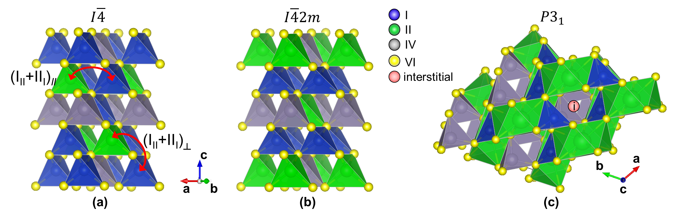
Cu2ZnSnS4 (CZTS) and Cu2CdSnS4 (CCTS) have similar zincblende-derived, tetrahedrally-coordinated structures ( kesterite and stannite respectively) with similar band gaps (1.4-1.5 eV). Cu2SrSnS4 (CSTS) and Cu2BaSnS4 (CBTS) have wider band gaps (2.0 eV) and crystallize in the trigonal structure where Cu and Sn are tetrahedrally coordinated but the larger II2+ cation is 8-fold coordinated (Fig. 1).
| Coord. | Ionic | Crystal | |||
|---|---|---|---|---|---|
| Cation | number | radius (Å) | compound | structure | |
| Cu+ | 4 | 0.60 | |||
| Sn4+ | 4 | 0.55 | |||
| Zn2+ | 4 | 0.60 | Cu2ZnSnS4 | 6.8 | |
| ” | ” | ” | Cu2ZnSnSe4 | 8.6 | |
| Cd2+ | 4 | 0.78 | Cu2CdSnS4 | ||
| Sr2+ | 8 | 1.26 | Cu2SrSnS4 | 6.1 | |
| Ba2+ | 8 | 1.42 | Cu2BaSnS4 | 6.1 | |
| Ag+ | 4 | 1.00 | Ag2ZnSnSe4 | 12.6 | |
| Ge4+ | 4 | 0.39 | Cu2ZnGeSe4 |
As mentioned above, an interesting feature of the CXTS series is the progressive increase of ionic radius of the X2+ cation from Zn2+ (0.60 Å) to Ba2+ (1.42 Å). The increasing ionic radius corresponds to an increasing size mismatch between the II2+ cation and both the Cu+ and Sn4+ cations (Table 1). Thus, classical intuition suggests that substituting Zn with the largest II2+ cations (Sr and Ba) presents an opportunity to reduce the concentration of various antisite defects, due to the high energetic cost of forming antisite defects between highly size-mismatched cations. Hong et al. (2016) Despite this potential advantage, the record efficiencies of CBTS and CSTS solar cells (2.0% and 0.6% respectively) Ge et al. (2017a); Crovetto et al. (2019) are much lower than those of CZTS and CCTS solar cells (11.0% and 8.0% respectively). Hadke et al. (2019); Yan et al. (2018)
In the first part of this work, we investigate chemical trends in the defect properties of the CXTS series by a combination of experimental techniques and first-principles calculations. Since defect spectroscopy measurements are not available in the literature for CBTS and CSTS, we start by performing temperature- and excitation dependent photoluminescence (PL) measurements on these materials and assign their shallow defect transitions to Cu vacancies and Cu interstitials by matching their measured ionization energies to the calculated charge transition levels. Across the whole Cu2-II-Sn-S4 series, we find that increasing the size of the II2+ cation leads to a smooth decrease in band tailing. In the second part of this work, we expand our investigation to a wider range of kesterite-inspired materials involving the substitution of other cations and anions. Analysis of their band tail trends suggests that Gaussian and Urbach tails in this class of materials have different chemical origins. Based on correlations between measured band tail parameters and calculated quantities, we tentatively assign Urbach tails to the (2III+IVI) defect clusters and Gaussian tails to the (III+III) defect cluster involving cations on different cationic planes. Finally, we conclude that non-radiative recombination and band tailing are largely decoupled from one another in kesterite-inspired materials. For example, CBTS and CSTS have more non-radiative losses than CZTS, although they exhibit significantly less band tailing.
II Experimental and computational details
CBTS and CSTS films on Mo-coated soda lime glass (SLG) were synthesized by sulfurization of oxide precursor films deposited by reactive sputtering. CZTS films on Mo-coated SLG were synthesized by sulfurization of sulfur-deficient CZTS films deposited by pulsed laser deposition. Details of the growth processes are available in previous publications. Crovetto et al. (2019, 2020); Cazzaniga et al. (2017) The elemental composition and sulfurization conditions of the films characterized in this work are those that gave the highest-efficiency cells in the previous studies. Crovetto et al. (2019, 2020); Cazzaniga et al. (2017) For all compounds, the bulk composition is Cu-poor and II-rich, and the sulfurization temperature is in the 520-560∘C range. For photoluminescence spectroscopy, the films were measured as-sulfurized without top contact layers. For external quantum efficiency measurements, a CdS/ZnO/ITO top contact was deposited by chemical bath deposition/RF sputtering/RF sputtering respectively.
Temperature-dependent and excitation intensity-dependent photoluminescence (PL) measurements were performed with a customized scanning microscopy setup based on a Nikon Eclipse Ti-U inverted microscope and a continuous wave (CW) 523 nm laser. The sample was placed inside a temperature controlled stage (HFS600, Linkam Scientific Instruments). Using a beam splitter, laser light was focused on the sample by a 10x objective lens and PL emission was collected by the same objective. The spot size was 11 m and the excitation intensity was 400 mW/mm2 for the temperature-dependent measurements. PL emission was filtered by a 550 nm long pass filter and directed to a spectrometer (Shamrock 303i, Andor) equipped with an electronically cooled CCD detector through a 250 m input slit. Additional PL spectra over a larger area (about 1 mm2) were used to quantify the relative PL intensity across various materials. An Accent RPM2000 system with 405 nm continuous-wave excitation laser at power density 500 mW/mm2 was used for this purpose. The external quantum efficiency (EQE) of the solar cells was measured using a PV Measurements QEXL setup calibrated with a reference Si photodiode.
Defect formation was probed from first-principles using the supercell approach. Calculations were performed based on density functional theory (DFT) Hohenberg and Kohn (1964); Kohn and Sham (1965) using the projector-augmented wave (PAW) method Blöchl (1994) and the hybrid exchange-correlation functional of Heyd-Scuseria-Ernzerhof (HSE06) Heyd, Scuseria, and Ernzerhof (2003) as implemented in VASP. Kresse (1999) The wave functions were expanded in plane waves up to an energy cutoff of 380 eV. The k-points were sampled according to a Monkhorst-Pack -mesh Monkhorst and Pack (1976) with a grid spacing less than 0.03 Å-1 for Brillouin zone integration. The atomic coordinates were relaxed until the forces were less than 0.01 eV/Å. The lattice vectors were optimized until residual stress was below 0.5 kbar. To eliminate the spurious electrostatic interactions between charged defects, finite size corrections Freysoldt, Neugebauer, and Van de Walle (2009); Kumagai and Oba (2014) were employed.
III Results and discussion
III.1 Photoluminescence features of Cu2-II-Sn-S4 compounds
PL features of CZTS have been extensively discussed in the literature Levcenko et al. (2016); Gershon et al. (2013); Grossberg et al. (2013); Tanaka, Shinji, and Uchiki (2014); Grossberg et al. (2012) and were recently summarized. Grossberg et al. (2019) Briefly, the PL peak of CZTS thin films at room temperature (RT) is broad and significantly red-shifted with respect to the band gap (FWHM and Stokes shift of more than 150 meV). Analysis of temperature-dependent and excitation power-dependent PL indicates strong spatial fluctuations in the band gap or the electrostatic potential of CZTS, or both. There is some consensus that the PL peak usually observed at RT can be attributed either to a band-to-impurity transition, also known as free-to-bound (FB), Levcenko et al. (2016) or a tail-to-impurity (TI) transition. Grossberg et al. (2012) Assignment to either transition may depend on how tail states are defined and on the specific samples being characterized. The impurity in these transitions is usually attributed to the CuZn acceptor or the ZnCu donor, both expected to be abundant and with compatible ionization energies. Chen et al. (2013) The pure selenide CZTSe has qualitatively similar PL features to the pure sulfide CZTS, although its room-temperature Stokes shift and peak width are generally smaller than in the pure sulfide, and the defect involved in the FB transition is generally shallower. In fact, some authors argue that impurities in CZTSe are too shallow to be distinguishable from the overall tail states, at least at RT. Rey et al. (2018a) Band-to-band (BB) transitions are rarely detected in CZTS and CZTSe by PL, although they have been reported in both compounds under high excitation intensity at RT. Chagarov et al. (2016); Grossberg et al. (2013); Tanaka, Shinji, and Uchiki (2014)
PL features of CCTS have also been discussed in the literature, although less extensively than for CZTS. Hadke et al. (2019); Pilvet et al. (2017) Similarly to the case of CZTS, the main room-temperature PL peak of CCTS is broad, strongly Stokes-shifted, and attributed to a FB transition. However, a narrower band-to-band peak is clearly observed in high-quality films. Hadke et al. (2019) PL features of CBTS and CSTS have not been analyzed in detail, Ge et al. (2017b); Crovetto et al. (2019, 2020) so in the the next two sections we will discuss temperature- and excitation dependent PL measurements on our own CBTS and CSTS films.
III.1.1 Photoluminescence of CBTS
PL spectra of CBTS are complex, with at least five distinct peaks recognizable at 79 K (Fig. 2(a)). We will propose a possible interpretation of PL features and related defects based on the data in Fig. S1, Supporting Information using the interpretation rules listed in Ref. 46. The results will be summarized in Table 2. Plots of the integrated peak areas (), peak widths (FWHM) and peak positions () as a function of temperature and excitation intensity are considered. Siebentritt (2006) Additional supporting data is provided by the exponent of the power law (Fig. S1(d)) and the activation energy of shallow defect levels obtained by least-squares fitting of Arrhenius plots of (Fig. S1(b)). Finally, the energy shift between a pair of peaks, or between a peak and the band gap energy can be useful for determining defect levels. All reported values are based on least-squares peak fitting using Gaussian functions with three fitting parameters (peak area, FWHM, and position).
Two narrow peaks at 2.038 eV and 2.065 eV are observed at 79 K, with peak positions independent of excitation intensity (Fig. S1(e)). Their narrow linewidth is typical of excitonic transitions Siebentritt (2006) using the model of a series of Wannier excitons with S orbitals. Assignment to the first and second free exciton of CBTS is excluded because the higher-energy peak has roughly the same intensity of the lower-energy peak. Instead, we assign the peak at 2.065 eV to a free exciton (FX) and the peak at 2.038 eV to a bound exciton (BX) similarly to the case of Cu-rich CuGaSe2. Bauknecht et al. (2000) The possible origin of the defect involved in the BX peak will be discussed later. The FX peak broadens and red-shifts with increasing temperature, with a position of 2.022 eV at RT (Fig. S1(a)). On the other hand, the BX peak becomes difficult to distinguish already at 100 K due to thermal ionization of the involved defect. Band-to-band (BB) recombination often takes over excitonic recombination in inorganic semiconductors with a low exciton binding energy and a high dielectric constant as the temperature is increased. Siebentritt (2006); Larsen et al. (2011) This change in recombination mechanism can be detected by the shift of the FX/BB peak versus temperature. The net effect of two phenomena determines the thermal peak shift: 1) the temperature-dependent band gap change, and 2) a blue shift given by when BB recombination takes over FX recombination. We find that the FX peak of CBTS red-shifts by 43 meV between 79 K and RT, in good agreement with the known temperature coefficient of the CBTS band gap. Ge et al. (2017a) We estimate the exciton binding energy of CBTS as meV from the hydrogen model using our calculated dielectric constant of 6.1 and average electron- and hole effective masses of 0.22 and 0.92 , respectively Zhu et al. (2017); Pandey and Jacobsen (2018) ( is the electron rest mass). A blue shift of 65 meV would be quite substantial, yet it is not observed in Fig. S1(a).
Hence, we conclude that the dominant PL peak of CBTS at RT is a (broadened) excitonic transition, as in layered halide perovskites and in many organic semiconductors. Ishihara, Takahashi, and Goto (1990); Würfel and Würfel (2010) The relatively low and relatively high in CBTS may be responsible for the persistence of excitonic transitions up to RT. This conclusion can explain the characteristic dip in the RT absorption coefficient of CBTS just above the band gap, which is typical of excitonic absorption Ishihara, Takahashi, and Goto (1990) and has been observed in nearly all previous studies of CBTS. Ge et al. (2017a, b); Crovetto et al. (2020); Shin et al. (2017) If the RT absorption onset is due to excitonic absorption, band gap extraction by means of Tauc plots is not justified and leads to underestimation of the band gap. Fitting the absorption coefficient with an Elliott function is a more appropriate method to extract the band gap in the presence of excitonic absorption. Elliott (1957) Based on the value of estimated above, we suggest that the RT band gap of CBTS is 70-100 meV higher than the values previously estimated using Tauc plots. Ge et al. (2017a, b); Crovetto et al. (2020); Shin et al. (2017)
The peak at 1.9 eV is the dominant PL feature at 79 K but it quenches with increasing temperature. At RT, it is merely detectable as a shoulder of the dominant FX peak. The Arrhenius plot in Fig. S1(b) shows that the 1.9 eV peak quenches quickly between 79 K and 120 K, then it is approximately constant in intensity between 120 K and 200 K, and it finally quenches again above 200 K. This behavior cannot be easily explained for a single transition, so we conclude that the 1.9 eV peak is the convolution of two different peaks and we fit each of them with a Gaussian function up to 120 K. In this low-temperature range, both peaks red-shift with increasing temperature to a slightly larger amount than expected from thermal band gap narrowing. The position of the higher-energy peak is independent of excitation intensity, whereas the lower-energy peak blue-shifts by 10 meV/decade (Fig. S1(e)), suggesting that band tails exist in this temperature range due to band edge fluctuations. Siebentritt (2006) Thus, we identify the lower-energy peak as a quasi-donor-acceptor-pair (QDAP) peak and the higher energy peak as a tail-to-impurity (TI) transition which becomes dominant when the shallow defect of the QDAP transition becomes thermally ionized. The shallow defect level can be extracted from the TIQDAP offset, which is meV in the temperature range where both peaks are detected (Fig. S1(a)). This value should is in good agreement with the activation energy of the QDAP peak, which is estimated as meV from a single exponential Arrhenius fit ( in Fig. S1(b)). As the temperature increases, the TI peak blue-shifts in the 175-225 K range but does not shift further at higher temperatures. This behavior is very similar to the temperature evolution of the QDAP/TI peak in Cu-poor CuGaSe2 Larsen et al. (2011) and can be explained by flattening of the band edge fluctuations in the region where the blue shift occurs. At temperatures above 225 K, band tails can be considered negligible so tail-to-impurity recombination effectively turns into band-to-impurity recombination, which is usually labeled as free-to-bound (FB) recombination. The mechanism responsible for band tail flattening at intermediate temperatures can be hypothesized by observing that the FWHM of PL peaks in CBTS generally increases with excitation intensity at low temperatures (Fig. S1(c)). If free carrier screening was the dominant mechanism the FWHM would decrease instead, Rey et al. (2018a); Lang et al. (2017) so tail state filling by photocarriers is a more likely mechanism. The impurity involved in the TI/FB transition is the same as the deep defect involved in the QDAP transition. This defect level can be extracted from the offset between the band gap energy (estimated as FX) and the FB peak position at temperatures 225 K, where band edge fluctuations are flattened and thus do not influence the FB peak energy. This offset is meV, in good agreement with the activation energy of meV (Fig. S1(b)) obtained by fitting the thermal quenching of the TI/FB peak with the equation
| (1) |
where is a constant, is a rate parameter, is the activation energy, and is the thermal energy.
Two additional low-intensity peaks can be detected at around 1.65 eV and 1.35 eV at low temperatures. They cannot simply be phonon replicas of the TI/FB peak because they would require much higher phonon wavenumbers than the ones found experimentally in CBTS (below 400 cm-1). Ge et al. (2017a); Crovetto et al. Thus, these peaks must be related to other radiative transitions in CBTS involving deeper defects. Small peak shifts versus excitation intensity are difficult to determine reliably for such low-intensity peaks. However, both peaks red-shift with increasing temperature similarly to the QDAP and TI peaks (Fig. S1(a)), they exhibit rather small coefficients (Fig. S1(d)), and their activation energies are much lower than those expected for such deep defects (Fig. S1(b)). Therefore, we identify both peaks as QDAP transitions between a rather shallow defect (corresponding to the observed activation energy) and a deeper defect which cannot be thermally ionized at these temperatures. Since a deep defect is involved, we label the 1.65 eV and 1.35 eV peaks as DDAP1 and DDAP2 respectively, meaning deep DAP transitions. The activation energy of the DDAP1 peak, extracted with Eq. 1, is meV, suggesting that the shallow defect involved in the DDPA1 transition may be the same defect that is also responsible for the TI/FB transition. Due to the limited available temperature range, the intensity of the DDAP2 peak is simply fitted with the equation, yielding meV. This value is similar to the activation energy of the shallower defect involved in the QDAP transition, again suggesting the same chemical origin for both defects. The ionization energy of the deep defects involved in the two DDAP transitions can be estimated as
| (2) |
where (FX) is the low-temperature band gap, DDAPx is the DDAP peak position, is the activation energy of its shallower defect (as determined above) and is the average tail depth at one of the band edges. Estimating meV based on the blue shift of the TI/FB peak at intermediate temperatures (Fig. S1(a)), ionization energies of meV and meV are derived for the deeper defects of the DDAP1 and DDAP2 transitions, respectively.
In conclusion, we have identified two shallow defects of opposite type (donor and acceptor) with ionization energies of about 40 meV and 135 meV. PL measurements alone cannot establish which is a donor and which is an acceptor. We have also identified two deeper defects with 300 meV ionization energy (same type as the 40 meV defect) and 700 meV ionization energy (same type as the 135 meV defect). These results are summarized in Table 2. Band edge fluctuations exist in CBTS at low temperatures, but they are not sufficiently strong to dissociate excitons. The related tail states are filled by photocarriers at temperatures above 200 K.
| CBTS: Experiment | CBTS: Theory | ||
|---|---|---|---|
| Exp. quantity | (meV) | Defect | (meV) |
| Cui(D1) | 118 | ||
| K)FB | ” | ” | |
| ” | ” | ||
| (FXBX) | ” | ” | |
| VCu(A1) | 63 | ||
| FBQDAP | ” | ” | |
| ” | ” | ||
| Eq. 2 (DDAP1) | A2 | ?? | |
| Eq. 2 (DDAP2) | D2 | ?? | |
III.1.2 Photoluminescence of CSTS
As for the case of CBTS, interpretation of PL features in CSTS requires detailed analysis based on the data in Fig. S2, Supporting Information. The results will be summarized in Table 3. Two main PL features are observed in CSTS at 83 K (Fig. 2(b)): a feature at 2.0 eV with a clear high-energy shoulder, and a broad asymmetric feature in the 1.2-1.7 eV range. Each feature can be fitted with two Gaussian peaks. The positions of the Gaussian peaks in the 2.0 eV feature are about 1.96 eV and 2.06 eV, with negligible excitation intensity- and temperature dependence up to 150 K (Figs. S2(a,e)). We assign the 1.96 eV peak to a TI transition (TI1) as in CBTS. Although it seems logical to identify the 2.06 eV as a FX or BB peak, there are two trends that are inconsistent with such an assignment. First, the TI1 peak has a higher coefficient than the 2.06 eV peak (Fig. S2(d)), which is in contrast with the corresponding coefficients in CBTS (Fig. S2(d)) and is not expected for a defect-related transition versus a non-defect-related transition. Siebentritt (2006) Second, the 2.06 eV peak remains at a constant position until 175 K and then it red-shifts by a much larger amount than the expected thermal band gap narrowing (Fig. S1(a)). Hence, we assign the 2.06 eV peak to a band-to-tail (BT) transition instead. Similarly to the case of CBTS, the TI peak of CSTS blue-shifts in the 150-200 K temperature range and then follows the red shift of the FX peak above 200 K. As in CBTS, we interpret the 30 meV blue shift at intermediate temperatures as flattening of band edge fluctuations. However, there is an important qualitative difference between the two materials. Namely, the FWHM of most peaks in CSTS decreases with excitation intensity, instead of increasing as in CBTS. This behavior is compatible with electronic screening of band edge fluctuations by photocarriers, rather than state filling. Rey et al. (2018a); Lang et al. (2017) As band edge fluctuations flatten, the BT peak turns into a FX peak and the TI1 peak turns into a FB peak (FB1), which quenches and leaves the FX peak as the dominant peak at RT. The dominance of a FX peak in CSTS at RT is compatible with the excitonic feature observed in the absorption coefficient of CSTS at RT. Crovetto et al. (2019) As for CBTS, this calls for a re-evaluation of the band gap of CSTS using an Elliott function, since standard Tauc analysis is not applicable and results in band gap underestimation. The exciton binding energy of CSTS is estimated as 62 meV using our calculated static dielectric constant of 6.1 and previously calculated average effective masses (0.22 for electrons and 0.82 for holes). Pandey and Jacobsen (2018); Zhu et al. (2017) Assuming the same temperature dependence of the band gap as in CBTS, the BT peak lies 24 meV below the estimated low-temperature band gap of CSTS, in good agreement with the tail state depth estimated by the blue shift of the TI peak (30 meV). PL transitions involving defects that are shallower than the band tails would merge with tail emission, so the existence of shallow defects with ionization energy 30 meV cannot be confirmed nor excluded.
| CSTS: Experiment | CSTS: Theory | ||
|---|---|---|---|
| Exp. quantity | (meV) | Defect | (meV) |
| (83 K)BT | ? | Cui(D1?) | 0 |
| BTTI1 | VCu(A1) | 70 | |
| FB2DDAP | ” | ” | |
| ” | ” | ||
| BTTI2 | D2 | ?? | |
The ionization energy of the (less shallow) defect involved in the TI1/FB1 transition can be estimated based on the shift between the BT and the TI1 peaks at low temperatures ( meV) or from the activation energy of the FB1 peak. However, the latter has an extremely large standard error ( meV) because the FB1 transition only begins to quench at relatively high temperatures (Fig. S2(b)), so we discard it in our analysis. The broad PL feature in the 1.2-1.7 eV range peak can also be fitted with two separate Gaussian peaks centered at 1.36 eV and 1.46 eV at 83 K. The peaks quench at different rates at higher temperatures, so that the lower-energy (high-energy) peak is dominant at low (high) temperatures. Above 160 K, the intensity of the low-energy peak is too low to be determined reliably, so we only fit the higher-energy peak with a single Gaussian function. Unlike the case of CBTS, this peak is still clearly visible at RT (Fig. 2(b)). The 1.46 eV peak does not shift with excitation intensity or with increasing temperature, whereas a small blue shift with excitation intensity and temperature is observed for the 1.36 eV peak. Thus, we assign the 1.46 eV peak to a TI peak transition involving a deep impurity and we assign the 1.36 eV peak to a DDAP transition. Similarly to the TI1 peak, the TI2 peak turns into a FB transition (FB2) at higher temperatures where band edge fluctuations flatten out. Thermal quenching of the TI2/FB2 and DDAP peaks can be fitted with Eq. 1, yielding activation energies of meV and meV for the TI2/FB2 peak and the DDAP peak, respectively (Fig. S2(b)). The former activation energy cannot be related to ionization of the (much deeper) defect involved in the TI2/FB2 transition, and is probably related to the activation of a competing non-radiative recombination channel instead. The ionization energy of this defect can, however, be estimated as meV based on the shift between the BT peak and the TI2 peak. On the other hand, the activation energy of the DDAP peak ( meV) is in good agreement with the ionization energy of the TI1/FB1 defect so we conclude that: (i) the shallow defect involved in the DDAP transition is the same defect responsible for the TI1/FB1 transition, and (ii) the deep defect involved in the DDAP transition is the same 600 meV defect responsible for the the TI2/FB2 transition. Consistent with this interpretation, the shift between the TI2 and the DDAP peak ( meV) is in good agreement with the activation energy of the DDAP peak.
To conclude, we have identified a shallow defect (110 meV ionization energy) and a deeper defect of opposite type (600 meV ionization energy) in CSTS. Since band edge fluctuations are present at low temperature, the existence of shallow defects with ionization energy 30 meV cannot be confirmed nor excluded. These results are summarized in Table 3. Similarly to CBTS, the tail states caused by band edge fluctuations are relatively shallow (30 meV) and seem to disappear at temperatures higher than 200 K.
III.2 Interpretation of defect levels in CBTS and CSTS
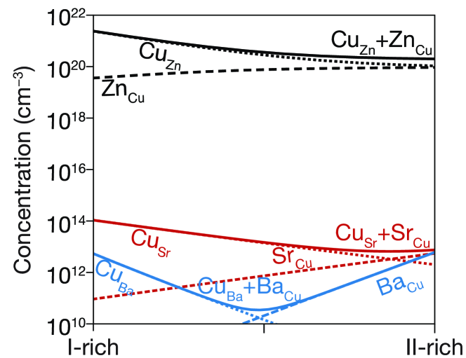
To investigate the possible chemical origin of the defects identified experimentally, we perform first-principles defect calculations. Previous work showed the single acceptor VCu and the single donor Cui to be the lowest-energy shallow defects in CBTS. Hong et al. (2016) We also find that VCu and Cui have shallow charge transition energies and much lower formation energies than the IICu donors and CuII acceptors (Fig. 3), which are expected to be 7 orders of magnitude less abundant than in CZTS and CCTS (Fig. 4). The particularly low formation energy of VCu favors p-type conductivity in both materials, as observed by experiment. Crovetto et al. (2019); Ge et al. (2017a) Compensation of VCu by the Cui donor is stronger in CSTS than in CBTS, which is consistent with a higher Fermi level position measured in CSTS with respect to its valence band maximum. Crovetto et al.
Since VCu and Cui are the most probable origin of the shallow defects identified by PL, we compare their calculated charge transition levels to the measured defect ionization energies in Table 2 and Table 3. In CBTS, meV for VCu and meV for Cui. These levels are in good agreement with the experimental ionization energies of 40 meV and 135 meV. Therefore, we assign the 40 meV level to the VCu acceptor and we assign the 130 meV level to the Cui donor as shown in Fig. 5. This assignment can be substantiated by analysis of the bound excition peak observed in CBTS (BX in Fig. 2(a)). The bound exciton involves a defect with ionization energy (BX-FX), where BXFX = 27 meV is the shift between the two excitonic peaks in Fig. 2(a) and is Haynes’ constant, which depends on the defect type and can be determined from the ratio of the effective masses of CBTS. Sharma and Rodriguez (1967); Atzmüller, Fröschl, and Schröder (1979) Assuming the same effective masses that we used for the estimation of , Zhu et al. (2017); Pandey and Jacobsen (2018) three possibilities exist. If the exciton was bound to an ionized impurity, the ionization energy of the latter would be 27 meV as for both donors and acceptors. Sharma and Rodriguez (1967) If the exciton was bound to a neutral impurity, the ionization energy of the latter would be 135 meV for a donor or 360 meV for an acceptor. Atzmüller, Fröschl, and Schröder (1979) The best match with the experimentally detected defects in Table 2 is between the 135 meV neutral donor expected by Haynes’s rule and the 135 meV defect found by PL analysis, which was also assigned to a donor based on our computational results. This donor is expected to be neutral at the temperature where the bound exciton peak is detected (79 K) because thermal quenching of the FB peak, corresponding to donor ionization, occurs at a much higher temperature.
The situation in CSTS is reversed, as the calculations predict VCu to be deeper than Cui. The calculated transition energies of the two defects (70 meV and 0 meV) suggest that the experimentally-determined 105 meV defect may be attributed to the VCu acceptor. Note that Cui is predicted to be extremely shallow, so it is in practice invisible to PL characterization even if present in a large concentration because of band edge fluctuations in CSTS at low temperature. Assignment of the deeper radiative levels to specific point defects is more difficult for both materials. The 300 meV acceptor in CBTS is potentially compatible with the charge transition levels of the the Si and SCu single acceptors, which were identified as the lowest-energy deep acceptors in a previous calculation. Hong et al. (2016) The ionization energies of the 700 meV and 600 meV deep donors found in CBTS and CSTS do not match the charge transition energy of any low-formation energy donors. Hong et al. (2016) The origin of these defects is unknown.
III.3 Defect trends in Cu2-II-Sn-S4 compounds
The shallow defects identified from PL transitions of CZTS and CZTSe are often assigned to cation antisites, typically ZnCu or CuZn. Their formation energies and charge transition levels are similar to those of the equivalent CdCu and CuCd antisites in CCTS. Yuan et al. (2015); Hadke et al. (2019) Furthermore, the characteristics of the room-temperature FB peak in CCTS are similar to those of the corresponding PL peak in CZTS Hadke et al. (2019) so it likely that antisites are responsible for shallow defect PL emission in CCTS as well. On the other hand, the large size of the Sr2+ and Ba2+ cations combined with their unique coordination number in the structure (Table 1) makes formation of II2+-based antisites energetically unfavorable (Fig. 4). Instead, VCu and Cui are likely to be the main shallow defects involved in radiative transitions in CBTS and CSTS, as discussed in the previous section.
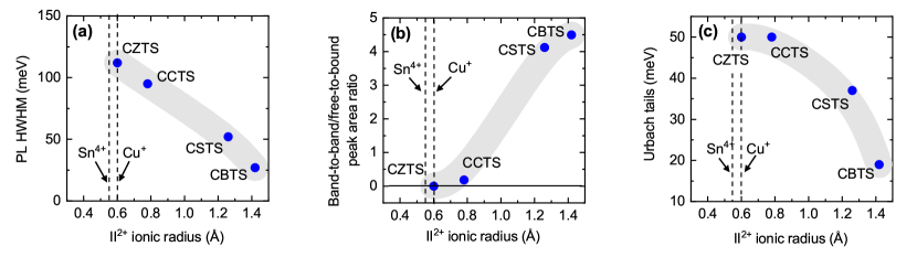
Apart from these differences in the dominant radiative defects, it is interesting to verify whether the ionic radius of the II2+ cation in the Cu2-II-Sn-S4 series is a good descriptor of the extent of band tailing in these materials, as originally hypothesized. Hong et al. (2016) We start by observing that lower band tailing in CBTS and CSTS with respect to the rest of the series cannot simply be explained by better dielectric screening, because their static dielectric constant is lower than in CZTS (Table 1). Three correlations can instead be provided, which seem to confirm the hypothesized role of the cationic radius. The first (Fig. 6(a)) is a simple correlation between the low-energy-side half-width at half-maximum (HWHM) of the main room-temperature PL peak and the II2+ ionic radius. The low-energy side of the PL spectrum corresponds to the density of the states involved in PL emission. In a tail-free material, the PL HWHM is simply due to the thermal distribution of carriers in the bands. Siebentritt (2006) In the presence of tail states, the HWHM increases to reflect the tail density of states. The behavior of the PL HWHM across the Cu2-II-Sn-S4 series confirms that tail states become shallower as the ionic radius of the II2+ cation deviates more and more from the ionic radii of Cu+ and Sn4+. A second correlation (Fig. 6(b)) involves the relative weight of the FB and the BB (or exciton) PL peaks at RT. In the presence of tail states or shallow defects that recombine radiatively, the intensity of the BB peak is reduced due to competition with tail- and defect-related transitions. Again, the trend in the Cu2-II-Sn-S4 series is consistent with a decrease in tail state- and shallow defect density as the I+-II2+ cation size mismatch increases going from Zn2+ to Ba2+. Finally, Urbach and Gaussian tails of the various compounds can be extracted directly from analysis of the solar cell’s external quantum efficiency (EQE) as shown in Fig. 7. Plotting the Urbach energy versus the II2+ ionic radius results again in the expected trend. Note that the Gaussian band gap distribution is also a decreasing function of the ionic radius, although Gaussian tails of CZTS are much larger, for reasons that will be discussed later. In conclusion, the tail state chemical trend in the Cu2-II-Sn-S4 series suggests that introducing size-mismatched cations is a successful strategy to mitigate band tailing in Cu2-II-Sn-S4 compounds, which further indicates that some type of antisite defect is the main cause of band tails in this class of materials. In the next section, the specific origin of band tails is investigated.
III.4 Tail state trends in kesterite-inspired materials
We now extend our discussion of band tails to include other kesterite-inspired materials involving substitution of Cu, Sn, and S, and attempt to understand the origin of band tails based on chemical trends. The origin of band tails in CZTS and CZTSe has been a heavily debated subject, which has not been entirely resolved. Two basic issues are important. The first is whether to attribute band tails to potential fluctuations or to band gap fluctuations. Potential fluctuations are the classical mechanism behind band tail formation in heavily compensated semiconductors. They are caused by a high concentration and non-random distribution of acceptors and donors, causing fluctuations in the electrostatic potential and non-local PL transitions between spatially separated potential wells for electrons and holes. Shklovskii and Efros (1984) Band gap fluctuations could be caused by the precipitation of binaries or ternary phases, Siebentritt and Schorr (2012) by competition between different crystal structures with similar energy and different band gaps (e.g. kesterite and stannite), Persson (2010); Siebentritt and Schorr (2012) or by the band gap narrowing effect of certain defect clusters. Chen et al. (2013) The most recent studies seem to suggest that band gap fluctuations, rather than potential fluctuations, are responsible for the majority of band tails in CZTSe. Rey et al. (2018a); Lang et al. (2017) These conclusions are mainly based on observations of the broadening of the low-energy side of the PL spectrum versus excitation intensity. If potential fluctuations were the only contribution to band tails, increased electrostatic screening due to the increasing free carrier concentration would cause peak narrowing with increasing excitation intensity. If band gap fluctuations were the only contribution, increased state filling with increasing excitation intensity would cause either no change to the low-energy side width, or possibly some broadening with increasing excitation intensity due to contributions from a more diverse set of defects. Rey et al. (2018a) However, no or very limited narrowing is observed experimentally, pointing to the predominant role of band gap fluctuations. Rey et al. (2018a); Lang et al. (2017)
The second issue in the band tail discussion is its chemical origin. Some researchers Gershon et al. (2013); Scragg et al. (2016); Nishiwaki et al. (2018) have attributed band tailing to Cu-Zn disorder owing to the abundance of the (CuZn+ZnCu) defect cluster, evidenced in Fig. 4. This can result both in band gap fluctuations due to the narrowing effect of the (CuZn+ZnCu) cluster on the band gap, Scragg et al. (2016) or in potential fluctuations due to the non-random distribution of CuZn acceptors and ZnCu donors. Gershon et al. (2013); Gokmen et al. (2013) However, other researchers have shown that band tails are independent of the order parameter of kesterite, thus excluding a major involvement of the (CuZn+ZnCu) cluster. Bourdais et al. (2016); Rey et al. (2018a) An often-invoked alternative chemical origin of the band tails is the (2CuZn+SnZn) defect cluster. Rey et al. (2018a); Hadke et al. (2019); Ma et al. (2019) According to first-principles calculations, Chen et al. (2013) this defect cluster has a low formation energy and causes significant band gap narrowing in CZTS. Its role in the experimentally observed band tails in kesterite is plausible but has not been proven experimentally so far.
In this section, we will take a different approach to the analysis of the causes of band tailing in kesterite-related materials. Our method is based on the analysis of band tail data over a chemical space containing various kesterite-inspired materials, and its comparison to calculated defect properties for those materials. This approach relies on the recent publication of experimental band tail data for various fully-substituted, kesterite-inspired semiconductors including CZTS, Hadke et al. (2019); Yan et al. (2017); Nishiwaki et al. (2018) CZTSe, Rey et al. (2018a); Hages, Carter, and Agrawal (2016); Nishiwaki et al. (2018) CZTSSe, Rey et al. (2018a); Gershon et al. (2016b); Gokmen et al. (2013) CCTS, Hadke et al. (2019) Ag2ZnSnSe4 (AZTSe), Gershon et al. (2016b) and Cu2ZnGeSe4 (CZGSe). Sahayaraj et al. (2017); Nagaya et al. (2018) It also relies on the availability of detailed defect calculations for CZTS, CZTSe, CCTS, and Ag2ZnSnS4 (AZTS). Chen et al. (2013); Yuan et al. (2015) The results of these calculations can be compared quantitatively, since they were performed by the same group using the same computational approach. Formation energies and band gaps of competing crystal structures are also available for various kesterite-inspired materials as a single consistent data set. Chen et al. (2010); Pandey and Jacobsen (2018)
Two clearly distinct types of experimental band tail data can be found. The first is a measure of the abruptness of optical absorption around the absorption onset, which can be derived either by optical measurements or by external quantum efficiency (EQE) measurements. To obtain an explicit quantity, one can take the derivative of EQE with respect to photon energy from below the absorption onset and up to its first inflection point (i.e., the maximum of the derivative) and fit it with a half-Gaussian function. The standard deviation of the Gaussian function can be interpreted as the standard deviation of the band gap distribution in the material. Mattheis, Rau, and Werner (2007) In Fig. 7(a) we perform this analysis on the EQE of CBTS, CSTS, and CZTS solar cells presented in previous work. Crovetto et al. (2019, 2020); Cazzaniga et al. (2017) Clearly, the Gaussian distribution of band gaps in CSTS and especially in CBTS is much narrower than in CZTS.
The second type of band tail data involves plotting at photon energies below the main absorption onset and fitting it with a straight line to extract the Urbach energy, which is the characteristic constant of a single-exponential tail. Hages, Carter, and Agrawal (2016) A similar method can be employed using the absorption coefficient of the material on a logarithmic scale, although a measurement technique which is sensitive to very low absorption coefficients must be used. Rey et al. (2018b); Malerba et al. (2014) In Fig. 7(b) we perform this analysis on the EQE measured on the same CBTS, CSTS, and CZTS solar cells as above. The result is qualitatively similar to the Gaussian analysis, with CBTS having a lower Urbach energy than CSTS, which in turn has a much lower Urbach energy than CZTS.
The Urbach energies and Gaussian band gap standard deviations measured for various kesterite-inspired materials are plotted against each other in Fig. 7(c). Materials based on substitutions of all four elements are included. We observe that the Urbach energy and the band gap standard deviation coincide only for certain materials, i.e., the ones that line up on the red line in Fig. 7(c). For other materials (CZGSe, CZTSe, and CZTS) the band gap standard deviation is larger than the Urbach energy by various amounts. Based on this trend, we propose that the Gaussian band gap distribution and the Urbach tails in CZTS, CZTSe, and CZGSe are not simply two possible models to quantify the same tailing phenomenon. Gokmen et al. (2013) Instead, Gaussian tails and Urbach tails are two separate phenomena which have distinct physical origins and coexist in (as a minimum) CZGSe, CZTSe and CZTS. As will be shown in the following paragraphs, establishing this distinction is very important in order to find the most plausible causes of band tails in kesterite-inspired materials. Our approach to identify the origin of both types of tails is to correlate either the band gap standard deviation or the Urbach energy to computationally available quantities related to defects or competing phases. Among them, we considered the following: (1) the calculated formation energy of various point defects and defect clusters that are known for CZTS, CZTSe, CCTS, and AZTS, such as I, II, IVII, (III + III), (2III + IVII); Chen et al. (2013); Yuan et al. (2015) (2) the calculated band gap narrowing (one defect per 128 crystal atoms) of various defect clusters, such as the (III + III) and (2III + IVII) listed above; Chen et al. (2013); Yuan et al. (2015) (3) the energy difference between the lowest-energy crystal structure and the second-lowest energy crystal structure; Chen et al. (2010); Pandey and Jacobsen (2018) and (4) the difference between the band gaps of the lowest-energy crystal structure and of the second-lowest energy crystal structure. Chen et al. (2010); Pandey and Jacobsen (2018)
We find that Urbach tails in CZTS, CZTSe, CCTS, and AZTSe are clearly not correlated to any of the investigated quantities, with the exception of band gap narrowing caused by the (2III + IVII) defect cluster (Fig. 8(a)). This correlation can be rationalized by remembering that Urbach tails are usually appropriate to model tail states that extend relatively deep into the forbidden gap. Rey et al. (2018a) In comparison to the (III + III) cluster, the (2III + IVII) cluster is less abundant but has a much larger influence on the local band gap. Chen et al. (2013) The observed correlation is in line with the assignment of several authors, e.g. Rey et al, Rey et al. (2018a) and Hadke et al., Hadke et al. (2019) who proposed (2CuZn + SnZn) as the main responsible for band tailing in kesterite. The large difference between the calculated gap narrowing (hundreds of meV) and the measured Urbach energies (tens of meV) need not be regarded as an inconsistency, because band gap narrowing was calculated assuming a certain defect concentration (one cluster per 128 crystal atoms) which is higher than the expected concentration of the (2III + IVII) cluster given its formation energy. Furthermore, Urbach tails describe exponentially decaying states, so the Urbach energy does not represent the deepest states involved in band tailing.
Since Gaussian tails are known to give a better description of relatively shallow tails with a large density of states, Rey et al. (2018a) one may expect to find some sort of correlation between the band gap standard deviation and the properties of the (III + III) cluster or of the corresponding individual defects. However no such correlation is found, with the main inconsistency being the behavior of CCTS. More precisely, the (III + III) cluster has about the same formation energy and gap narrowing effect in CCTS and in CZTS, Yuan et al. (2015); Chen et al. (2013); Hadke et al. (2019) but the band gap standard deviation in CCTS is about one half of the one in CZTS. On the other hand, we find a correlation between the standard deviation of band gaps and the energy difference between the ground state structure and the second lowest-energy structure (Fig. 8(b)), but only for the materials in which the latter has a lower band gap than the former. In all the materials that meet this requirement (CTZS, CZTSe, AZTSe, CZGSe) this corresponds to the energy difference between the ground state kesterite structure () and the stannite structure (), as shown in Table 4. Conversely, in CCTS the ground state is stannite and the second lowest-energy structure is kesterite. In CBTS and CSTS, the ground state is and the second lowest-energy structure is , which has a wider band gap (Table 4). This correlation can be rationalized as follows. All the materials that line up on the red line in Fig. 7(c) are the materials in which the most stable structure has a lower band gap than the second most stable structure (CSTS, CBTS), or in which the second most stable structure has a large energy difference with the most stable structure (AZTSe). In these materials, inclusion of the second most stable structure is either negligible in concentration, or it only modifies the absorption coefficient of the single-phase material above its absorption onset and therefore band tails are not detected using the method shown in Fig. 7(a). Importantly, inclusion of the second structure does not result in potential wells that can trap carriers, such as the previously described (2III + IVII) defect cluster. For the materials that deviate from the red line in Fig. 7(c), the ease of formation of the lower-band gap stannite polymorph is a good descriptor of the extra Gaussian contribution to the band tails as illustrated in Fig. 8(b).
This correlation requires further discussion. As mentioned above, the (CuZn+ZnCu) defect cluster has often been blamed for band tails in kesterite, Gershon et al. (2013); Scragg et al. (2016); Nishiwaki et al. (2018) a hypothesis that has been disproved by several authors. Rey et al. (2018a); Malerba, Valentini, and Mittiga (2017) However, closer examination reveals that many possible configurations of (CuZn+ZnCu) clusters can exist, depending on the location of the swapping atoms. Scragg et al. (2016); Nishiwaki et al. (2018) The lowest-energy configuration involves swapping of Cu and Zn atoms within the Cu-Zn planes (1/4 or 3/4) of the kesterite structure (Fig. 1(a)). We will label this in-plane cluster configuration as (CuZn+ZnCu)∥. The (CuZn+ZnCu)∥ cluster is the one reported in Fig. 4 of the present paper and in our reference defect calculations. Yuan et al. (2015); Chen et al. (2013) The (CuZn+ZnCu)∥ configuration is responsible for the much-discussed cation disorder in CZTS, as it can be sufficiently abundant to be detected directly by, e.g., neutron diffraction. Schorr et al. (2019) In fact, complete cation disorder in the 1/4 and 3/4 planes is achieved when there is one (CuZn+ZnCu)∥ cluster per 16 atoms (or two unit cells). Among all the conceivable (CuZn+ZnCu) cluster configurations and concentrations, this completely disordered configuration has the lowest energy, only 0.3 meV/atom higher than the defect-free CZTS kesterite structure. Scragg et al. (2016) However, many other cluster configurations and concentrations are possible. A particularly interesting configuration is the out-of-plane (CuZn+ZnCu)⟂ cluster, where one Cu atom from a Cu-Sn plane (0, 1/2, or 1) swaps with a Zn atom from a Cu-Zn plane. Formation of one (CuZn+ZnCu)⟂ cluster per 64 atoms (8 unit cells) costs 3.7 meV/atom more than forming a defect-free CZTS kesterite structure. Scragg et al. (2016) There are two important features of the (CuZn+ZnCu)⟂ cluster. First, its formation energy is low but not as low as for the (CuZn+ZnCu)∥ cluster, indicating that it should be present in very high concentrations with respect to most other defects but it may be still difficult to detect in the refinement step of x-ray or neutron diffraction experiments. Second, the presence of (CuZn+ZnCu)⟂ clusters can be interpreted as a partial transition from the kesterite to the stannite structure. In fact, it can be seen from Fig. 1 that the stannite structure is equal to a kesterite structure with one (CuZn+ZnCu)⟂ defect cluster per unit cell.
From the above discussion, we propose that the additional Gaussian band tails observed in materials with the kesterite crystal structure are due either to ”true” stannite inclusions or to a high density of (III+III)⟂ defect clusters, which are related to a partial transition to a stannite structure. The formation energy of (III+III)⟂ clusters is only available for CZTS so it cannot be used for correlation purposes across multiple materials. However, the energy difference between stannite and kesterite structures can be considered a good descriptor of such a formation energy and can support the role of (III+III)⟂ clusters in the correlation observed in Fig. 8(b). These hypotheses are compatible with the outcome of previous studies Rey et al. (2018a); Malerba, Valentini, and Mittiga (2017) which concluded that band tails in CZTS and CZTSe do not depend on the order parameter. The reason is that the order parameter is sensitive to (CuZn+ZnCu)∥ cluster concentrations but not necessarily to (CuZn+ZnCu)⟂ cluster concentrations or to the fraction of stannite present in the kesterite matrix. However, in a more general sense the III and III defects are still responsible for the Gaussian contribution to the band tails in the materials with a kesterite ground state structure CZTS, CZTSe, CZGSe, and AZTSe. Since the ground state structure of CCTS is stannite, Gaussian tails in CCTS are much less pronounced than in CZTS despite the nearly identical formation energy of the (III+III)∥ cluster in the two materials.
| Ref. 69 | Ref. 12 | Ref. 12 | |
| material | (meV/at.) | (meV/at.) | (meV/at.) |
| AZTSe | |||
| CZGSe | |||
| CZTSe | |||
| CZTS | |||
| CCTS | 3.2 | 4.7 | +100 |
| CSTS | 35.2 | +100 | |
| CBTS | 51.1 | +130 |
III.5 Deep defects and non-radiative recombination trends in kesterite-inspired materials
Fig. 8(c) shows the relative PL intensity of various kesterite-inspired semiconductors. According to Planck’s law, Würfel and Würfel (2010) PL intensity depends exponentially on the splitting between the electron and hole quasi-Fermi levels in the illuminated semiconductor, following the approximate relation , or . Here, is the thermal energy and is a constant reflecting the fact that the the PL intensities reported in Fig. 8(c) are in arbitrary units instead of as a quantum yield. Defining the voltage loss due to non-radiative recombination as , where is the maximum open-circuit voltage according to the Shockley-Queisser limit, it follows that every order of magnitude increase in corresponds to a mV decrease in the non-radiative loss . Comparing PL intensities across various materials is then equivalent to comparing differences in their non-radiative voltage losses.
Note that the data in Fig. 8(c) was compiled from different sources, where the PL intensities of various absorbers were measured relative to one another. Hadke et al. (2019); Gurieva et al. (2020); Crovetto et al. (2019, 2020) Thus, the data is to be intended only as semi-quantitative, as error bars up to one order of magnitude are expected for the relative PL intensity of material pairs that were not compared directly in the same study. It should also be noted that different excitation intensities may have been used in the different studies. However, the exponents in the power laws at RT are similar (around 1.3-1.4) for most of the materials shown in Fig. 8(c). This ensures that the relative intensity trends are roughly preserved using different excitation intensities.
Some interesting qualitative conclusions can be drawn from Fig. 8(c). First, PL intensity is clearly not correlated to the measured band gap standard deviation, indicating that non-radiative recombination and band tails are independent of each other. In other words, a given material may have a low density of defects responsible for band tailing but that doesn’t imply a low density of efficient non-radiative recombination centers. For example, band tails in CBTS are quite shallow compared to most other kesterite-inspired materials but its non-radiative recombination loss is about 115 mV larger than in CZTS since its PL intensity is about two orders of magnitude lower. A second important conclusion is related to the materials design principle based on intentionally employing size-mismatched cations to discourage the formation of antisite defects. The introduction of the large Ba2+ and Sr2+ cations in CBTS and CSTS does prevent the formation of some antisite defects (Figs. 4 and 6) but it clearly aggravates non-radiative recombination losses, as evidenced by a particularly low PL intensity in CBTS and CSTS (Fig. 8(c)). We speculate that interstitial defects, which generally have high formation energies in kesterite or stannite materials, Chen et al. (2013); Yuan et al. (2015) may be abundant in CBTS and CSTS due to the characteristics of the structure (Fig. 1(c)). Specifically, the eight sulfur atoms surrounding the II2+ cation in the structure form square antiprisms. The squared faces of the antiprisms are rather distant from one another, leaving an open ”cage” where an interstitial atom can be accommodated without a large perturbation of the crystal structure. In CBTS, a S interstitial located between two antiprisms would be 3.20 Å away from eight other sulfur atoms, which is not much closer than the equilibrium distance between sulfur atoms in the structure of CBTS (3.52 Å). It is also important to note that defects with 600 meV ionization energy have been identified in CBTS and CSTS by PL characterization in this study (Fig. 5). With some rare exceptions Grossberg et al. (2014) such deep defects are usually not detected by PL in materials with the kesterite structure. Hence, we conclude that deep defects and non-radiative recombination are a serious issue in the -structured CBTS and CSTS compounds.
IV Conclusion
To better understand the fundamental loss mechanisms of kesterite-inspired photovoltaic materials, we investigated the chemical trends in the defect properties of the Cu2-II-Sn-S4 (CXTS) series by a combination of experimental techniques and first-principles calculations. Three main conclusions were reached. First, the dominant shallow defects in CBTS and CSTS are Cu vacancies (acceptors) and Cu interstitials (donors) instead of the CuII and IICu antisites that are prominent in CZTS. Second, band tailing in the CXTS series decreases gradually as the size mismatch between the II2+ cation and the other cations increases. Third, mitigation of band tailing does not imply mitigation of non-radiative recombination rates. On the contrary, deep defects are more prominent and non-radiative recombination losses more severe in CBTS and CSTS than in CZTS, despite their much less pronounced band tails.
Then, we took a broader look at the family of kesterite-inspired semiconductors and suggested that deep Urbach tails and shallow Gaussian tails may have fundamentally different origins in this class of materials. Urbach tails are correlated with the calculated band gap narrowing caused by (2III+IVII) defect clusters. Gaussian tails are correlated with the energy difference between the kesterite and stannite polymorphs in the materials having kesterite as the lowest-energy structure. Noticing that the transformation from kesterite to stannite is equivalent to the formation of (III+III)⟂ defect clusters across cationic planes, we suggest that Gaussian tails may be caused by these out-of-plane clusters. Unlike the (III+III)∥ clusters responsible for the well-known cation disorder in kesterite, the different arrangement of (III+III)⟂ clusters implies that they do not cause disorder in the I-II plane, which is the experimentally available measure of the (III+III) defect concentation. This subtle difference can explain why various studies have found a lack of correlation between cation disorder and band tails in kesterite. Our results provide clear criteria for selecting tail-state-free photovoltaic absorbers in the vast I2-II-IV-VI4 chemical space.
Acknowledgements
This project has received funding from the European Union’s Horizon 2020 research and innovation programme under the Marie Skłodowska-Curie grant agreement No 840751, and from VILLUM Fonden (grant no. 9455). The Center for Nanostructured Graphene is sponsored by the Danish National Research Foundation (Project No. DNRF103). The PL imaging setup has been partly funded by the IDUN Center of Excellence funded by the Danish National Research Foundation (project no. DNRF122) and VILLUM Fonden (grant no. 9301). This research has also been funded by the EU Horizon2020 Framework (STARCELL, Grant No. 720907). We are grateful to the UK Materials and Molecular Modelling Hub for computational resources, which is partially funded by EPSRC (EP/P020194/1). Via our membership of the UK’s HEC Materials Chemistry Consortium, which is funded by EPSRC (EP/L000202), this work used the ARCHER UK National Supercomputing Service (http://www.archer.ac.uk).
V References
References
- Giraldo et al. (2019) S. Giraldo, Z. Jehl, M. Placidi, V. Izquierdo‐Roca, A. Pérez‐Rodríguez, and E. Saucedo, Advanced Materials 31, 1806692 (2019).
- Crovetto et al. (2018) A. Crovetto, A. Cazzaniga, R. B. Ettlinger, J. Schou, and O. Hansen, Solar Energy Materials and Solar Cells 187, 233 (2018).
- Crovetto et al. (2017) A. Crovetto, M. L. N. Palsgaard, T. Gunst, T. Markussen, K. Stokbro, M. Brandbyge, and O. Hansen, Applied Physics Letters 110, 083903 (2017).
- Chen et al. (2013) S. Chen, A. Walsh, X.-G. Gong, and S.-H. Wei, Advanced Materials 25, 1522 (2013).
- Kim et al. (2019) S. Kim, J.-S. Park, S. N. Hood, and A. Walsh, Journal of Materials Chemistry A 7, 2686 (2019).
- Hages et al. (2017) C. J. Hages, A. Redinger, S. Levcenko, H. Hempel, M. J. Koeper, R. Agrawal, D. Greiner, C. A. Kaufmann, and T. Unold, Advanced Energy Materials 7, 1700167 (2017).
- Rey et al. (2018a) G. Rey, G. Larramona, S. Bourdais, C. Choné, B. Delatouche, A. Jacob, G. Dennler, and S. Siebentritt, Solar Energy Materials and Solar Cells 179, 142 (2018a).
- Kim et al. (2020) S. Kim, J. A. Márquez, T. Unold, and A. Walsh, Energy Environ. Sci. 13, 1481 (2020).
- Gokmen, Gunawan, and Mitzi (2014) T. Gokmen, O. Gunawan, and D. B. Mitzi, Applied Physics Letters 105, 033903 (2014).
- Wang et al. (2014) C. Wang, S. Chen, J.-H. Yang, L. Lang, H.-J. Xiang, X.-G. Gong, A. Walsh, and S.-H. Wei, Chemistry of Materials 26, 3411 (2014).
- Shin, Saparov, and Mitzi (2017) D. Shin, B. Saparov, and D. B. Mitzi, Advanced Energy Materials , 1602366 (2017).
- Pandey and Jacobsen (2018) M. Pandey and K. W. Jacobsen, Physical Review Materials 2, 105402 (2018).
- Giraldo et al. (2018) S. Giraldo, E. Saucedo, M. Neuschitzer, F. Oliva, M. Placidi, X. Alcobé, V. Izquierdo-Roca, S. Kim, H. Tampo, H. Shibata, A. Pérez-Rodríguez, and P. Pistor, Energy Environ. Sci. 11, 582 (2018).
- Cabas-Vidani et al. (2018) A. Cabas-Vidani, S. G. Haass, C. Andres, R. Caballero, R. Figi, C. Schreiner, J. A. Márquez, C. Hages, T. Unold, D. Bleiner, A. N. Tiwari, and Y. E. Romanyuk, Advanced Energy Materials 8, 1801191 (2018).
- Gershon et al. (2016a) T. Gershon, Y. S. Lee, P. Antunez, R. Mankad, S. Singh, D. Bishop, O. Gunawan, M. Hopstaken, and R. Haight, Advanced Energy Materials 6, 1502468 (2016a).
- Sahayaraj et al. (2017) S. Sahayaraj, G. Brammertz, B. Vermang, T. Schnabel, E. Ahlswede, Z. Huang, S. Ranjbar, M. Meuris, J. Vleugels, and J. Poortmans, Solar Energy Materials and Solar Cells 171, 136 (2017).
- Hadke et al. (2019) S. Hadke, S. Levcenko, G. Sai Gautam, C. J. Hages, J. A. Márquez, V. Izquierdo‐Roca, E. A. Carter, T. Unold, and L. H. Wong, Advanced Energy Materials , 1902509 (2019).
- Shin et al. (2017) D. Shin, T. Zhu, X. Huang, O. Gunawan, V. Blum, and D. B. Mitzi, Advanced Materials 29, 1606945 (2017).
- Ge et al. (2017a) J. Ge, P. Koirala, C. R. Grice, P. J. Roland, Y. Yu, X. Tan, R. J. Ellingson, R. W. Collins, and Y. Yan, Advanced Energy Materials 7, 1601803 (2017a), arXiv:1404.7572 .
- Crovetto et al. (2019) A. Crovetto, R. Nielsen, E. Stamate, O. Hansen, B. Seger, I. Chorkendorff, and P. C. K. Vesborg, ACS Applied Energy Materials 2, 7340 (2019).
- Hautier et al. (2011) G. Hautier, C. Fischer, V. Ehrlacher, A. Jain, and G. Ceder, Inorganic Chemistry 50, 656 (2011).
- Shannon (1976) R. D. Shannon, Acta Crystallographica Section A 32, 751 (1976).
- Persson (2010) C. Persson, Journal of Applied Physics 107, 053710 (2010).
- Gershon et al. (2017) T. Gershon, O. Gunawan, T. Gokmen, K. W. Brew, S. Singh, M. Hopstaken, J. R. Poindexter, E. S. Barnard, T. Buonassisi, and R. Haight, Journal of Applied Physics 121, 174501 (2017).
- Hong et al. (2016) F. Hong, W. Lin, W. Meng, and Y. Yan, Physical Chemistry Chemical Physics 18, 4828 (2016).
- Yan et al. (2018) C. Yan, J. Huang, K. Sun, S. Johnston, Y. Zhang, H. Sun, A. Pu, M. He, F. Liu, K. Eder, L. Yang, J. M. Cairney, N. J. Ekins-Daukes, Z. Hameiri, J. A. Stride, S. Chen, M. A. Green, and X. Hao, Nature Energy 3, 764 (2018).
- Crovetto et al. (2020) A. Crovetto, K. Børsting, R. Nielsen, A. Hajijafarassar, O. Hansen, B. Seger, I. Chorkendorff, and P. C. K. Vesborg, ACS Applied Energy Materials 3, 1190 (2020).
- Cazzaniga et al. (2017) A. Cazzaniga, A. Crovetto, C. Yan, K. Sun, X. Hao, J. Ramis Estelrich, S. Canulescu, E. Stamate, N. Pryds, O. Hansen, and J. Schou, Solar Energy Materials and Solar Cells 166, 91 (2017).
- Hohenberg and Kohn (1964) P. Hohenberg and W. Kohn, Physical Review 136, B864 (1964).
- Kohn and Sham (1965) W. Kohn and L. J. Sham, Physical Review 140, A1133 (1965).
- Blöchl (1994) P. E. Blöchl, Physical Review B 50, 17953 (1994).
- Heyd, Scuseria, and Ernzerhof (2003) J. Heyd, G. E. Scuseria, and M. Ernzerhof, The Journal of Chemical Physics 118, 8207 (2003).
- Kresse (1999) G. Kresse, Physical Review B 59, 1758 (1999).
- Monkhorst and Pack (1976) H. J. Monkhorst and J. D. Pack, Physical Review B 13, 5188 (1976).
- Freysoldt, Neugebauer, and Van de Walle (2009) C. Freysoldt, J. Neugebauer, and C. G. Van de Walle, Physical Review Letters 102, 016402 (2009).
- Kumagai and Oba (2014) Y. Kumagai and F. Oba, Physical Review B 89, 195205 (2014), arXiv:1402.1226 .
- Levcenko et al. (2016) S. Levcenko, J. Just, A. Redinger, G. Larramona, S. Bourdais, G. Dennler, A. Jacob, and T. Unold, Physical Review Applied 5, 024004 (2016).
- Gershon et al. (2013) T. Gershon, B. Shin, N. Bojarczuk, T. Gokmen, S. Lu, and S. Guha, Journal of Applied Physics 114, 154905 (2013).
- Grossberg et al. (2013) M. Grossberg, P. Salu, J. Raudoja, and J. Krustok, Journal of Photonics for Energy 3, 030599 (2013).
- Tanaka, Shinji, and Uchiki (2014) K. Tanaka, T. Shinji, and H. Uchiki, Solar Energy Materials and Solar Cells 126, 143 (2014).
- Grossberg et al. (2012) M. Grossberg, J. Krustok, J. Raudoja, and T. Raadik, Applied Physics Letters 101, 102102 (2012).
- Grossberg et al. (2019) M. Grossberg, J. Krustok, C. J. Hages, D. M. Bishop, O. Gunawan, R. Scheer, S. M. Lyam, H. Hempel, S. Levcenco, and T. Unold, Journal of Physics: Energy 1, 044002 (2019).
- Chagarov et al. (2016) E. Chagarov, K. Sardashti, A. C. Kummel, Y. S. Lee, R. Haight, and T. S. Gershon, The Journal of Chemical Physics 144, 104704 (2016).
- Pilvet et al. (2017) M. Pilvet, M. Kauk-Kuusik, M. Grossberg, T. Raadik, V. Mikli, R. Traksmaa, J. Raudoja, K. Timmo, and J. Krustok, Journal of Alloys and Compounds 723, 820 (2017).
- Ge et al. (2017b) J. Ge, P. J. Roland, P. Koirala, W. Meng, J. L. Young, R. Petersen, T. G. Deutsch, G. Teeter, R. J. Ellingson, R. W. Collins, and Y. Yan, Chemistry of Materials 29, 916 (2017b).
- Siebentritt (2006) S. Siebentritt, in Wide-Gap Chalcopyrites, Vol. 86, edited by S. Siebentritt and U. Rau (Springer, Berlin, Heidelberg, 2006) pp. 113–156.
- Bauknecht et al. (2000) A. Bauknecht, S. Siebentritt, J. Albert, Y. Tomm, and M. C. Lux-Steiner, Japanese Journal of Applied Physics 39, 322 (2000).
- Larsen et al. (2011) J. K. Larsen, K. Burger, L. Gutay, and S. Siebentritt, in 2011 37th IEEE Photovoltaic Specialists Conference (IEEE, 2011) pp. 000396–000401.
- Zhu et al. (2017) T. Zhu, W. P. Huhn, G. C. Wessler, D. Shin, B. Saparov, D. B. Mitzi, and V. Blum, Chemistry of Materials 29, 7868 (2017).
- Ishihara, Takahashi, and Goto (1990) T. Ishihara, J. Takahashi, and T. Goto, Physical Review B 42, 11099 (1990).
- Würfel and Würfel (2010) P. Würfel and U. Würfel, Physics of solar cells, 3rd ed. (Wiley-VCH Verlag GmbH, Wenheim, 2010).
- Elliott (1957) R. J. Elliott, Physical Review 108, 1384 (1957).
- Lang et al. (2017) M. Lang, C. Zimmermann, C. Krämmer, T. Renz, C. Huber, H. Kalt, and M. Hetterich, Physical Review B 95, 155202 (2017).
- (54) A. Crovetto, Z. Xing, M. Fischer, T. Rindzevicius, R. Nielsen, N. Stenger, D. Scanlon, I. Chorkendorff, and P. C. K. Vesborg, submitted .
- Sharma and Rodriguez (1967) R. R. Sharma and S. Rodriguez, Physical Review 153, 823 (1967).
- Atzmüller, Fröschl, and Schröder (1979) H. Atzmüller, F. Fröschl, and U. Schröder, Physical Review B 19, 3118 (1979).
- Yuan et al. (2015) Z.-K. Yuan, S. Chen, H. Xiang, X.-G. Gong, A. Walsh, J.-S. Park, I. Repins, and S.-H. Wei, Advanced Functional Materials 25, 6733 (2015).
- Shklovskii and Efros (1984) B. I. Shklovskii and A. L. Efros, Electronic properties of doped semiconductors (Springer, Berlin, 1984).
- Siebentritt and Schorr (2012) S. Siebentritt and S. Schorr, Progress in Photovoltaics: Research and Applications 20, 512 (2012).
- Gershon et al. (2016b) T. Gershon, K. Sardashti, O. Gunawan, R. Mankad, S. Singh, Y. S. Lee, J. A. Ott, A. Kummel, and R. Haight, Advanced Energy Materials , 1601182 (2016b).
- Scragg et al. (2016) J. J. S. Scragg, J. K. Larsen, M. Kumar, C. Persson, J. Sendler, S. Siebentritt, and C. Platzer Björkman, physica status solidi (b) 253, 247 (2016).
- Nishiwaki et al. (2018) M. Nishiwaki, K. Nagaya, M. Kato, S. Fujimoto, H. Tampo, T. Miyadera, M. Chikamatsu, H. Shibata, and H. Fujiwara, Physical Review Materials 2, 085404 (2018), arXiv:1803.05106 .
- Gokmen et al. (2013) T. Gokmen, O. Gunawan, T. K. Todorov, and D. B. Mitzi, Applied Physics Letters 103, 103506 (2013).
- Bourdais et al. (2016) S. Bourdais, C. Choné, B. Delatouche, A. Jacob, G. Larramona, C. Moisan, A. Lafond, F. Donatini, G. Rey, S. Siebentritt, A. Walsh, and G. Dennler, Advanced Energy Materials 6, 1502276 (2016).
- Ma et al. (2019) S. Ma, H. Li, J. Hong, H. Wang, X. Lu, Y. Chen, L. Sun, F. Yue, J. W. Tomm, J. Chu, and S. Chen, The Journal of Physical Chemistry Letters 10, 7929 (2019).
- Yan et al. (2017) C. Yan, K. Sun, J. Huang, S. Johnston, F. Liu, B. P. Veettil, K. Sun, A. Pu, F. Zhou, J. A. Stride, M. A. Green, and X. Hao, ACS Energy Letters 2, 930 (2017).
- Hages, Carter, and Agrawal (2016) C. J. Hages, N. J. Carter, and R. Agrawal, Journal of Applied Physics 119, 014505 (2016).
- Nagaya et al. (2018) K. Nagaya, S. Fujimoto, H. Tampo, S. Kim, M. Nishiwaki, Y. Nishigaki, M. Kato, H. Shibata, and H. Fujiwara, Applied Physics Letters 113, 093901 (2018).
- Chen et al. (2010) S. Chen, A. Walsh, Y. Luo, J.-H. Yang, X. G. Gong, and S.-H. Wei, Physical Review B 82, 195203 (2010).
- Mattheis, Rau, and Werner (2007) J. Mattheis, U. Rau, and J. H. Werner, Journal of Applied Physics 101, 113519 (2007).
- Rey et al. (2018b) G. Rey, C. Spindler, F. Babbe, W. Rachad, S. Siebentritt, M. Nuys, R. Carius, S. Li, and C. Platzer-Björkman, Physical Review Applied 9, 064008 (2018b).
- Malerba et al. (2014) C. Malerba, F. Biccari, C. L. Azanza Ricardo, M. Valentini, R. Chierchia, M. Müller, A. Santoni, E. Esposito, P. Mangiapane, P. Scardi, and A. Mittiga, Journal of Alloys and Compounds 582, 528 (2014).
- Malerba, Valentini, and Mittiga (2017) C. Malerba, M. Valentini, and A. Mittiga, Solar RRL 1, 1700101 (2017).
- Schorr et al. (2019) S. Schorr, G. Gurieva, M. Guc, M. Dimitrievska, A. Pérez-Rodríguez, V. Izquierdo-Roca, C. S. Schnohr, J. Kim, W. Jo, and J. M. Merino, Journal of Physics: Energy 2, 012002 (2019).
- Gurieva et al. (2020) G. Gurieva, J. A. Márquez, A. Franz, C. J. Hages, S. Levcenko, T. Unold, and S. Schorr, Physical Review Materials 4, 054602 (2020).
- Grossberg et al. (2014) M. Grossberg, T. Raadik, J. Raudoja, and J. Krustok, Current Applied Physics 14, 447 (2014).
SUPPORTING INFORMATION
The special case of band gap narrowing in AZTSe
In Fig. 8(a) of the main article, the calculated band gap narrowing due to the 2(III + IVII) defect cluster is plotted on the x-axis, based on the values calculated in Refs. 4; 57. The AZTSe data point is, however, a special case that needs further clarification. First, calculations of defect clusters are only available for AZTS and not for AZTSe and, second, the 2(AgZn + SnZn) cluster in AZTS has a very high formation energy. Yuan et al. (2015) As a worst-case scenario, we considered the defect cluster with the largest calculated band gap narrowing among low-formation-energy defects in AZTS, which is (SnZn + ZnSn). To extrapolate its band gap narrowing effect from AZTS to AZTSe we simply followed the trend of the (SnZn + ZnSn) defect from CZTS to CZTSe, as shown in Ref. 4. We consider this an acceptable approximation since all four compounds have the same crystal structure (kesterite) and exhibit the same band gap trend, i.e., a band gap decrease by 0.5 eV when replacing S with Se.
When going from CZTS to CZTSe, the valence band upshift is reduced by a factor 2, and the conduction band downshift is reduced by a factor of 4.Chen et al. (2013) Using these correction factors, the calculated band gap narrowing of AZTSe is extrapolated as 70 meV, which is the value plotted on the x-axis of Fig. 8(a) in the main article for the AZTSe data point. Note that the trend identified in Fig. 8(a) is still valid if a different defect cluster is chosen for AZTSe, because all the other calculated defect clusters narrow the band gap to a smaller extent than the (SnZn + ZnSn) cluster. Yuan et al. (2015)