Charge density wave and superconducting phase in monolayer InSe
Abstract
In this paper, the completed investigation of a possible superconducting phase in monolayer indium selenide is determined using first-principles calculations for both the hole and electron doping systems. The hole-doped dependence of the Fermi surface is exclusively fundamental for monolayer InSe. It leads to the extensive modification of the Fermi surface from six separated pockets to two pockets by increasing the hole densities. For low hole doping levels of the system, below the Lifshitz transition point, superconductive critical temperatures K are obtained within anisotropic Eliashberg theory depending on varying amounts of the Coulomb potential from 0.2 to 0.1. However, for some hole doping above the Lifshitz transition point, the combination of the temperature dependence of the bare susceptibility and the strong electron-phonon interaction gives rise to a charge density wave that emerged at a temperature far above the corresponding . Having included non-adiabatic effects, we could carefully analyze conditions for which either a superconductive or charge density wave phase occurs in the system. In addition, monolayer InSe becomes dynamically stable by including non-adiabatic effects for different carrier concentrations at room temperature.
I Introduction
Motivated by the discovery of graphene Novoselov et al. (2004), a two-dimensional (2D) advanced material with spectacular properties, researchers have greatly discovered 2D layered materials; namely, hexagonal boron nitride Kim et al. (2012), transition metal dichalcogenides (such as MoS2 and WS2) Chhowalla et al. (2013), magnetic 2D crystalline-like monolayer chromium triiodide (CrI3) Huang et al. (2017) and other elemental 2D semiconductors such as black phosphorus Li et al. (2014) and silicene Vogt et al. (2012), ranging from insulators, semiconductors, metals, magnetics and superconductors.
In addition, group III-VI semiconductors (M2X2, M = Ga and In and X = S, Se and Te) with sombrero-shaped valence band edges have shown marvelous electrical and optical properties Zólyomi et al. (2013, 2014). The bulk indium selenide (InSe), III-monochalcogenide semiconductor, has and structural phases depending on the stacking characteristics Han et al. (2014); Lei et al. (2014); Politano et al. (2017). Among these phases, has an indirect bandgap about eV Lei et al. (2014), while, and phases have a direct bandgap close to Gürbulak et al. (2014) and eV Julien and Balkanski (2003), respectively. Electron–phonon coupling (EPC) and the superconductive properties of an electron-doped monolayer InSe were studied Chen (2019) and a superconductive transition temperature about 3.41 K was reported. Moreover, it has been shown that hole states in monolayer InSe are strongly renormalized by coupling with acoustic phonons leading to the formation of satellite quasiparticle states near the Fermi energy Lugovskoi et al. (2019a). Not long ago, monolayer InSe has been fabricated from its bulk counterpart by mechanical exfoliation Mudd et al. (2013, 2014); Feng et al. (2015). High carrier mobility of about cm2/Vs, which is greater than that of MoS2 Cui et al. (2015), has been reported at room temperature Sun et al. (2016); Bandurin et al. (2017); suggesting that this 2D material is promising for ultra-thin digital electronics applications. Furthermore, InSe represents a promising material for making use of FETs Marin et al. (2018).
The presence of a sombrero-shaped valence band in the electronic band structure of monolayer InSe gives rise to a larger density of states (DOS), which is similar to that of one-dimensional material, and specifies a Van Hove singularity at the valence band maximum (VBM) which could primarily lead to a magnetic transition and superconducting phases as well Bardeen et al. (1957); Cao et al. (2015); Dresselhaus et al. (2007); Hung et al. (2017); Wu et al. (2014). Stimulated by the remarkable discovery of gate-induced superconductivity in graphene (upon lithium adsorption) Ludbrook et al. (2015); Ichinokura et al. (2016); Profeta et al. (2012); Xue et al. (2012), a new field for investigating superconducting features on other 2D materials typically has emerged. In advance, lithium adsorbed graphene was properly utilized for 2D superconductivity. Undoubtedly owing to a small DOS at the Fermi level and symmetry which gives rise to a weakened electron coupling with the flexural modes, graphene illustrates a small electron-phonon coupling constant, . However, these shortcomings could be lifted by typically making use of lithium adsorption Profeta et al. (2012); Xue et al. (2012).
Even though monolayer InSe naturally has symmetry, electrons in monolayer InSe could couple to the flexural phonons owing to the presence of atomic layers away from the symmetry plane. Notably, this coupling alongside a larger DOS near the VBM potentially leads to a significant EPC parameter. On the other hand, the active presence of a significant DOS as well as makes the system susceptible to a charge density wave (CDW) instability, which represents a static modulation of the itinerant electrons and usually accompanied by a periodic distortion of the lattice. The CDW formation may naturally arise from a possible combination of a large nesting and/or electron-phonon interaction at a specific phonon wave vector (). Therefore, the formation of the CDW must be carefully examined for systems with a strong EPC, though a superconducting state is possible.
The standard method of properly investigating CDW formation is first to calculate the phonon dispersion of the system within density functional theory (DFT) calculations, i.e. considering either a small displacement or density functional perturbation theory (DFPT) method at specific temperatures Baroni et al. (2001). It is worth mentioning that the long-wavelength electron-phonon interaction induced phonon self-energy is carefully considered in the phonon dispersion of both mentioned approaches Calandra et al. (2010). However, it has become evident that dynamical phonons undoubtedly play a significant role and non-adiabatic/dynamic effects could give rise to a significantly renormalized phonon dispersion for doped semiconducting materials Lazzeri and Mauri (2006); Saitta et al. (2008); Novko et al. (2019) including InSe.
Here, we investigate a viable superconducting and CDW phases of monolayer InSe based on DFT and necessary DFPT calculations. We calculate the renormalized phonon dispersion owing to the electron-phonon coupling in both adiabatic and non-adiabatic regimes for different temperatures and doping levels. We further investigate the competition between CDW formation and the superconductive phase for different hole and electron doping levels. We eagerly discuss the most important phonon wave vectors leading to the remarkable electron-phonon coupling strength which well expresses the significance of both bare susceptibility and the nesting function below and above the Lifshitz transition point. By including non-adiabatic effects, we carefully analyze conditions for which either a superconductive or CDW phase could typically emerge in the system. Our desired results show that in some hole-doped cases, CDW instability prevents access to quite high-temperature superconductivity, whereas for some other doped levels, the achievement of such superconducting temperatures is possible. In the electron-doped cases, the CDW instability is significantly suppressed, and therefore the superconducting phase is possible.
The paper is organized as follows. We commence with a description of our theoretical formalism in Sec. II, followed by the details of the DFT and DFPT calculations. Numerical results for the band structures, phonon dispersions, DOS, superconducting critical temperature, and CDW in adiabatic and non-adiabatic approximations are reported in Sec. III. We summarize our main findings in Sec. IV.
II Theory and computational details
Self-consistent DFT calculations are carefully performed with LDA-norm-conserving pseudopotential as implemented in the Quantum Espresso package Giannozzi et al. (2009). The phonon dispersion and self-consistent deformed potentials are calculated based on the DFPT method Baroni et al. (2001); Wierzbowska et al. (2005); Calandra et al. (2010). The Kohn-sham wave functions and Fourier expansion of the charge density are truncated at 90 and 360 Ry, respectively. To eliminate spurious interactions between adjacent layers, a vacuum space of 25 Å along the direction is adopted. For the electronic and phononic calculations, a k mesh and q-mesh, are used and a finer k mesh of and q mesh of , respectively, are applied to calculate the Wannier interpolation of the electronic and phonon dispersions as implemented in EPW code Marzari and Vanderbilt (1997); Souza et al. (2001); Mostofi et al. (2008); Poncé et al. (2016). The Dirac delta functions are approximated by applying a Gaussian smearing and . The convergence of results is carefully performed as a function of the k and q mesh and Gaussian smearing. Moreover, to adequately describe the temperature dependence of the electronic structure, the Fermi-Dirac smearing of about 0.01 Ry is used Verstraete and Gonze (2001).
Since the static part of the phonon self-energy is typically included in the phonon dispersion, one may uniquely define a dressed phonon frequency as Albertini et al. (2017),
| (1) |
where is the bare phonon frequency and is the static part of the first-order self-energy of phonon modes, refer to the electronic band indeces, is the considerable number of k points, is the electron-phonon interaction matrix elements and represents the Fermi-Dirac distribution function.
It is justifiable to assume k independent electron-phonon interactions in which . Therefore, Eq. (1) can be written as follows;
| (2) |
where is the bare charge susceptibility. Phonon softening typically emerges at some branches of the phonon spectrum, known as the Kohn anomaly Kohn (1959) which originates from any sizable variation of as a function of and/or the electronic temperature. Consequently, it is standard practice to scientifically verify as a necessary signature of the phonon softening and thus the formation of the CDW. The CDW instability can be well appeared in the form of an imaginary phonon band when the temperature lies below (the temperature where softened modes touch the zero frequency at ).
To estimate the superconducting temperature in systems with a strong EPC, we utilize the Migdal-Eliashberg formalism Migdal (1958); Eliashberg (1960) in the form of a modified Allen-Dynes parametrization Allen and Dynes (1975):
| (3) |
with , , is the Morel-Anderson Coulomb potential, in general, adopted in the range of 0.1-0.2, and and represent strong-coupling and shape corrections, respectively (for detailed definitions of and see Ref. Allen and Dynes (1975)). The Eliashberg function is defined as
| (4) | |||
where N() is the electronic density of states at the Fermi level. The imaginary part of the phonon self-energy reads as follows:
| (5) |
To carefully analyze the different contributions of and , the projected quantities are defined as follows. Two principal directions are typically considered: in-plane and out-of-plane distortions. The along the specific direction is written as
| (6) |
for the atom type in the unit cell (including In2 or Se2) where (labeled by in-plane), (labeled as out of plane), and
| (7) |
where vector is the eigenvector of the dynamical matrix. The can also be projected into Cartesian coordinates by making use of the phonon displacements associated with various atom types in different directions,
| (8) |
where refer to the in-plane and out-of-plane deformations, respectively with and and is the displacement pattern Not (a), so that satisfies the following relation
| (9) |
In particular, we define , and . Projected can be obtained by projected as follows:
| (10) |
It would be worth mentioning the Fermi surface of monolayer InSe is anisotropic for some doping levels implying the importance of using the anisotropic Eliashberg theory. In this regard, the in anisotropic equations Margine and Giustino (2013) was implemented as a cutoff independent quantity in EPW code. However, to get better consistent results comparable with that obtained by Eq. 3, we gain use of a cutoff dependent given by
| (11) |
where represents the number of Matsubara frequencies at a defined temperature and Allen and Dynes (1975); Not (b) is a good estimation. This approach provides better results compared with the one when is used Margine and Giustino (2013). The value of is obtained when the superconducting gap becomes smaller than eV.
Furthermore, in metallic systems, the ion dynamic affects the electron dynamics and leads to the excited state owing to the proximity of phonon energies and electron excited states Calandra et al. (2010). The experimental realization of such dynamics on the phonon energies is observable in the form of a Raman frequency shift at the zone center so-called non-adiabatic effects Novko et al. (2019); Saitta et al. (2008); Novko (2020); Giustino (2017). To explore this, a time-dependent perturbation theory (TDPT) is necessary for a full ab initio treatment of non-adiabatic effects. Since a full TDPT is complicated enough in practical terms of complexity of the accurate calculations, we adopt the following procedure, by pursuing Ref. Calandra et al. (2010), to properly include the non-adiabatic effects. As the first necessary step for a specific q vector, adiabatic self-consistent force constants, , are calculated. Here is the electronic temperature applied in self-consistent calculations ( is large enough to prevent a Kohn anomaly). The non-adiabatic phonons can be naturally obtained by diagonalizing the phonon dynamical matrix related to non-adiabatic non-self-consistent force constants, , at a physical temperature given by Calandra et al. (2010):
| (12) |
where comprises both the addition (subtraction) of non-adiabatic (adiabatic) effects at the specific temperature () used in the related Fermi-Dirac distribution function , respectively,
| (13) |
where is the k-point grid at smearing and much larger than and we consider as a positive real infinitesimal parameter. Furthermore, are deformation potential matrix elements which include the derivative of the Kohn-Sham self-consistent potential with respect to the Fourier transform of the phonon displacements Calandra et al. (2010). Therefore, to obtain phonon energies within an adiabatic regime a coarse k-point mesh and 1580 K as a proper starting point are considered. While a dense enough k-point grid of is adopted for the calculation of non-adiabatic and adiabatic force constant matrices at more reduced temperatures ().
III Numerical results and discussions
Two distinct types of structural phases ( and ) have been properly reported for pristine monolayer InSe in Ref. Zólyomi et al. (2014) whose phase has mirror symmetry, while has inversion symmetry. Moreover, both of them are dynamically stable, but, the former possesses cohesive energy slightly lower than the latter. We efficiently perform our DFT calculations on phase by incorporating a hexagonal structure with symmetry. The relaxed geometry calculations of pristine monolayer InSe show that the optimized hexagonal unit cell naturally has the lattice constant Å and two sublayers are separated by distance = 2.66 Å and = 5.15 Å. These parameters are in good agreement with those results reported in Zólyomi et al. (2014); Hung et al. (2017); Chen (2019).
| e/f.u. | charge density | (K) | (K) | ||||
|---|---|---|---|---|---|---|---|
| 0.15 | 0.20 | ||||||
| +0.01 | 0.758 | 7.62 | 4.26 | 123 | 65 | 58 | 51 |
| +0.04 | 3.0 | 7.36 | 8.05 | 106 | 55 | 48 | 42 |
| +0.1 | 7.58 | 6.99 | 8.30 | 90 | 44 | 38 | 34 |
| +0.2 | 15.1 | 3.07 | 3.02 | 79 | 21 | 17 | 15 |
| +0.3 | 22.6 | 1.44 | 1.50 | 78 | 9 | 8 | 7 |
| +0.4 | 30 | 0.85 | 0.76 | 80 | 4 | 3 | 2 |
| - 0.1 | 7.44 | 0.55 | 0.82 | 97 | 2 | 1 | 0 |
| - 0.2 | 14.6 | 0.50 | 0.63 | 103 | 2 | 1 | 0 |
III.1 Investigation of superconductive properties of monolayer InSe
In this work, both the electron- and hole-doped cases are studied within the jellium model for monolayer InSe. A compensate positive or negative background charge is included to guarantee the charge neutrality.
There are different experimental techniques like electrolytic gate
Efetov and Kim (2010) to precisely control the rate of the electron and hole densities. Here, we consider electron doping levels and electron per formula unit (e/f.u.) precisely corresponding to the electron densities, and cm-2 respectively. Similarly, (low doping regime), and e/f.u. (high doping regime) for hole-doped cases corresponding to , , , , and cm-2 charge densities are considered. For the sake of simplicity, we promptly drop e/f.u. units corresponding to various doping levels, refers to the hole/electron doping, respectively.
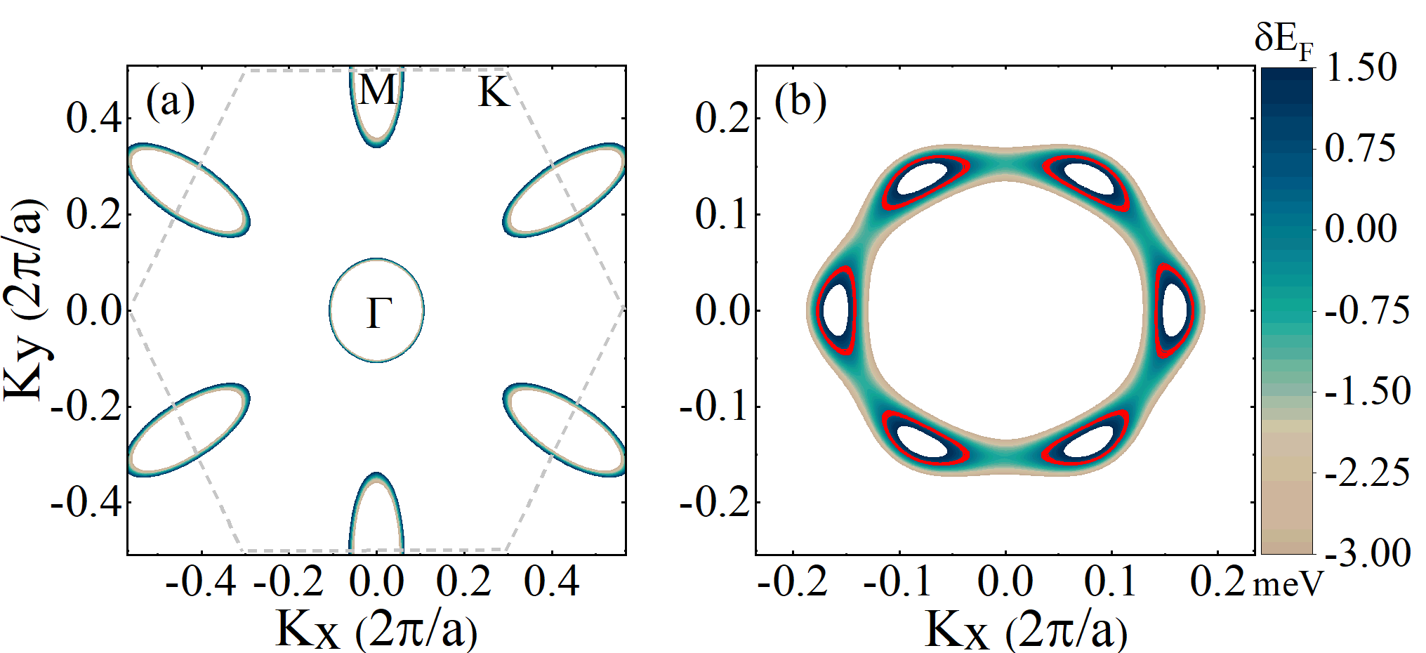
The Fermi surfaces of the system are described in Fig. 1 for different doping levels. Figure 1(a) displays the topology of the Fermi surface for doping consisting precisely of two types of electronic pockets located at the and points. In the case of the deeper electronic doping level , the specific form of the Fermi surface is similar to the previous doping level. The Fermi surface of the doping system consists of six separated pockets located around a point between the and K as shown in Fig. 1 marked by the red color.
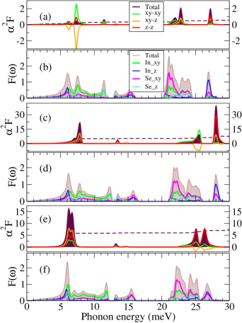
In the hole-doped case [see Fig. 1(b)] and upon more significantly decreasing the Fermi energy , a Lifshitz transition Zólyomi et al. (2014) occurs. Therefore, the topology of the Fermi surface with six pockets, located between and K, changes to two coaxial pockets around the point. This fundamental change of the principal character of the Fermi surface results in a tangible variation of the superconductive properties of the hole-doped system which we adequately address in the following. Moreover, this specific concentration is obtained to be equal to 5.8 or +0.076 e/f.u. which is in good agreement with that reported in Ref.Zólyomi et al. (2014). To begin with, we carefully look at the Eliashberg function in terms of various doping levels. Figures 2(a) and (b) depict the projected and phonon DOS for doping level . The projected Eliashberg function along the in-plane and out-of-plane deformations show a mighty peak at around 27 meV related to a scattering process which originates primarily from resulting from the out-of-plane vibration of In atoms and in-plane vibration of Se atoms. This is equally consistent with the projected in Fig. 2(b), where there is a significant density of phonons with Inz and Sexy deformations. Looking at more reduced energies there is a two-peak structure between meV, which comes from . On the other hand, peaks at more reduced energies originate from .
The and are shown in Figs. 2(c) and (d) for the low hole doping level . A peak around 28 meV comes principally from single optical phonon mode with out-of-plane In and in-plane Se vibrations. In this case, the deformation of is considerably larger than . Moreover, the lesser peak at around 26 meV has a major and a minor character with a negative contribution from , while the strong peak at around 8 meV has a major character with relatively similar contributions from the other two deformations.
As a notable example of high a hole-doped regime, the and projected for are shown in Figs. 2(e) and (f), respectively. Despite the low hole-doped and electron-doped cases, the prominent peak around 28 meV is absent. In general, the spectrum of hole-doped is slightly shrunk in comparison with the one. Moreover, the gapped two-peak structure in the high-energy part of the for is replaced with a gapless one at an energy of about 25-27 meV. The outstanding contribution of this high-energy part arises mainly from the and deformations, however, the has a completely negative contribution. The low-energy peak between 5-7 meV has almost an identical character to the low-energy peak of the doping level, albeit with a lesser height. Therefore, the peak of is shifted to lower energies by passing through the Lifshitz transition point (increasing hole doping levels). In addition, there is a tangible suppression of the proportion of the spectral weight of high-energy phonons to low-energy phonons. Such a modulation of optical phonons affects their superconductive properties, which mainly manifests itself in the suppression of (see Table. 1).
Looking at the cumulative in Figs. 2(a), (c) and (e), we can fairly state that in hole doping the acoustic branches carry out a more pronounced role in the formation of the . Unlike the hole-doped cases, for electron doping, there is a more uniform distribution of each branch contributing in the formation of the for the electron doping, as inferred from .
The tabulated amounts of with respect to various doped levels in Table. 1 reveal that increasing the hole/electron doping levels leads to a descending/constant behavior of , respectively.
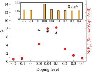
To perceive the correlation between the DOS at the Fermi energy and , we collect the results of Table. 1 into Fig. 3, where and are shown for different doping levels. Upon progressively increasing the hole density, while decreases monotonously, the increases up to doping level then decreases for a larger doping level.
One can seemly remark that can take an effect from and the average of the electron-phonon matrix elements on the Fermi surface, and effectively could be represented as , where is an average electron-phonon interaction. Therefore, if one considers the , it will be possible to recognize that the proportion is about unity for all doping levels but, +0.01 and 0.1,
for doping level 0.01 an enhancement of the average electron-phonon interaction is expected. To estimate the average electron-phonon interaction we use, , and the results of the are presented in the inset of Fig. 3. As seen, the average electron-phonon interaction is enhanced for +0.01, compared to the other hole and electron doping levels. Thus, in general, a larger DOS results in a larger with a linear dependency, with the only exception being the 0.01 doping level, where is enhanced in comparison with the other doping levels where it is almost constant.
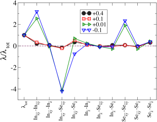
Furthermore, Eq. (10) is used to carefully consider the contribution of the projected for different atom types and the out-of/in-plane directions in the . Figure 4 shows the projected while those are rescaled to the for four doping levels and . The desired results show, for the electron-doped case, the highest contribution to the is attributed to the in-plane displacements. For the corresponding in-plane/out-of-plane contributions are .
For the hole-doped levels beyond +0.1, on the other hand, the largest contribution arises from the out-of-plane deformations and mixed in-plane In and out-of-plane Se deformations. For doping level +0.1 the projected s read, .
In the case of +0.01 doping, the system is somewhere between a greater hole doping and the electron-doped
cases. While its in-plane contributions share the same behavior as of the electron-doped one; its out-of-plane and mixed in-plane/out-of-plane contributions behave properly similar to the high doping levels, .
To be specific, the valuable contribution which comes from (In-Se) deformation has a negative impact for the electron-doped system, while it has a positive contribution for low and high hole-doped cases.
This key difference originates from the distinction between the generic forms of the topology of the Fermi surface such that this type of polarization is beneficial for hole-doped cases and it is a disadvantage for the electron-doped ones.
In addition, Table 1 shows the critical transition temperature to the superconducting phase with the aforementioned doped conditions calculated through Eq. (3) by considering three values for . In the case of hole doping, the highest value of K is obtained for . Our results reveal that can be shrunk about 20 percent when was applied.
Obviously, while the amount of is almost the same for the first three hole-doped cases, the for is larger than that of (by considering ); stemming from a larger value of . The larger value of the corresponding to the former originates from the fact that the phonon dispersion for doped is typically harder than . Moreover, the proportion of the high energy peak to the low-energy peak of for the case of +0.01 is appreciably larger than that of (see Figs. 2(c) and (e)). Thus, is enhanced for in comparison with .
| e/f.u. | (K) | (K) | (K) | ||
|---|---|---|---|---|---|
| 0.15 | 0.20 | ||||
| +0.01 | 73 | 64 | 54 | 122 | 2 |
| +0.04 | 75 | 68 | 62 | 145 | 2 |
| +0.1 | 55 | 50 | 43 | 416 | 120 |
| +0.2 | 20 | 17 | 15 | 539 | 191 |
| +0.3 | 9 | 8 | 7 | 476 | 246 |
| +0.4 | 4 | 3 | 2 | 2 | 2 |
| - 0.1 | 2 | 0 | 0 | 2 | 2 |
| - 0.2 | 2 | 1 | 0 | 2 | 2 |
Notice that the highest tabulated temperature is comparable with K for blue phosphorene studied in Ref. Esfahani and Asgari (2017). Moreover, it is much larger than the reported for Li-decorated monolayer graphene and antimonene with Ludbrook et al. (2015) and K Lugovskoi et al. (2019b), respectively. However, the high value of needs a careful examination and further insights into the formation of the CDW phase at low temperatures for the hole-doped system which we adequately address in the following section.
To have a better estimate of , we utilize a self-consistent solution of the anisotropic the Migdal-Eliashberg theory. The results are reported in Table. 2. Obviously, anisotropic effects alter at the first three hole-doped cases, where the Fermi surface has a more pronounced anisotropic character (see Fig. 1(b)), while a slight variation of is observed for other hole- and electron-doped cases when s are extracted from Allen-Dynes formula ( Eq. 3) and self-consistent anisotropic Eliashberg equations. These results indicate that below the Lifshitz transition point, in comparison with the Allen-Dynes estimate, the is more pronounced in comparison with the cases above the Lifshitz transition point as well as the electron doped levels. For the +0.04 doping level, such an anisotropy can enhance from a range 42-55 K corresponding to the Allen-Dynes estimate to 62-75 K for different applied .
III.2 CDW formation in adiabatic and non-adiabatic approximations
More reduction in the electronic temperature to achieve is alongside the giant amplitude of the Kohn anomaly. To acquire an estimate of , we extract the frequency of the most softened mode on the whole -mesh, for different temperatures, then we fit the extracted frequencies to Duong et al. (2015). In our calculations, is a constant close to 0.4 and yields values in the range 0.40-0.43 for all hole doping levels which are partly close to the value extracted from the mean-field approximation Duong et al. (2015); Gruner (1994). Figure 5 shows the variation of the phonon frequencies as a function of electronic temperature and related fitting curves (red dashed lines) for case +0.3 in both adiabatic and non-adiabatic regimes. The results indicate that the transition to the CDW region occurs in K and K. The values of corresponding to other doping levels, for both adiabatic and non-adiabatic regimes are reported in Table 2.
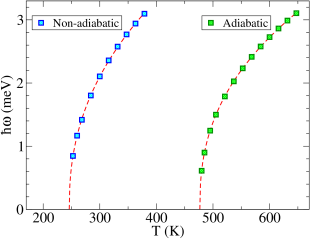
Figure 6 depicts the amplitude of the Kohn anomaly as a function of the electronic Fermi-Dirac smearing for doping level +0.1. Typically decreasing the temperature leads to a more softening of the phonon energies and finally, the system suffers from a CDW instability at a smearing slightly lower than 416 K. For exploring the considerable variations of the phonon softening as a function of the Fermi-Dirac smearing, three upper temperatures, 420, 470 and 1580, in the adiabatic/static regime are depicted. The typical smearing 1580 K, as a starting point in the adiabatic regime, is large enough to wipe out the Kohn anomaly in the linear response calculations. In addition, this figure shows there are two which give rise to two different chiralities. One includes a commensurate supercell corresponding to the dip in the middle of the - direction. The secondary point of the CDW instability is related to an incommensurate distortion precisely corresponding to another dip along the - path. Our numerical calculations reveal that the dip in the middle of the -K direction has a lower and we, therefore, refer to this point as in the reminder. Notice that for the other higher doped levels, i.e. and , the CDW forms at the same q for the +0.1 doping level. On the other hand, in the adiabatic regime, low hole doping levels +0.01 and +0.04 show instability in a q marginally different from the high doped regime. However, it does not show any instability of the system even at extremely low temperatures by including non-adiabatic effects as illustrated in Table 2. Besides, in the comparison between low doped and high doped regimes in terms of phonon softening at , we therefore report our results at for doping levels and as well.
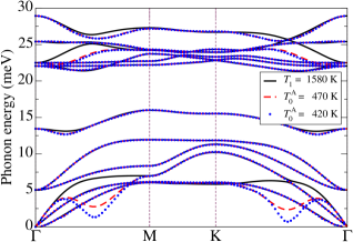
Figure 7 shows different quantities associated with the CDW formation for various doping levels and temperatures. In particular, the average amounts of the electron-phonon interaction , where the nesting function is precisely defined as , is properly used. The tilde symbol in Fig. 7 refers to the related calculations at the . Moreover, the depicted quantities are associated with the softened branch at , therefore, the branch index is dropped.
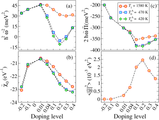
The effects of phonon energy renormalization as a function of temperature within the adiabatic/static regime are shown in Fig. 7(a). These results reveal the tendency of the system to the CDW region for the three , and doping levels. On the contrary, the electron-doped and low hole doping levels, below the Lifshitz transition point, almost retain their constant behavior as a function of various temperatures. Figure 7(b) shows the bare susceptibility as a function of doped levels at the for the aforementioned temperatures. Notice that the is the largest for doping level (see Fig. 7(d)), in addition, the largest change of the basically belongs to the doping level . This leads to a further decline of (from a temperature of 1580 K) for doping level as shown in Fig. 7(c). Moreover, such a larger variation in the for doping levels , and leads to a giant Kohn anomaly and finally the appearance of the instability in monolayer InSe for smearing lower than 416, 539 and 476 K, respectively. A comparison for doping implicitly expresses that though there is a reduction of the self-energy correction, having less temperature dependence on together with a smaller average of (Fig. 7(d)) on the Fermi surface, results in less effective Kohn anomaly and therefore, the CDW is suppressed at for doping level .
Further analyses associated with the polarization of the softened mode at adequately explain the instability at this point mainly involves the in-plane displacements of the In atoms and the out-of-plane displacements of the Se atoms at the same time.
The notable absence of the Kohn anomaly for an electron doping is owing to the lack of a reduction of the with respect to the different temperatures alongside an extremely small (Fig. 7(d)). In two low hole doping cases, is smaller than that obtained for other hole-doped levels. For doping level a specific combination of a small and the lack of typically decreasing of as a function of temperature results in the absence of the Kohn anomaly at . In doping level , although there is a depletion in upon temperature reduction, due to a slight value of , it sufficiently shows a smaller softening.
Therefore, considering the adiabatic regime, competition and coexistence between and , reveals that is exceedingly greater than and consequently, the CDW instability prevents access to the high-temperature superconductivity in the first five hole-doped cases +0.01, +0.04, +0.1, +0.2 and +0.3. On the other hand, in the intra-sheet scattering process, when , the substantional difference of the non-adiabatic and adiabatic frequencies is which approximately specifies at the Fermi surface Novko et al. (2019); Saitta et al. (2008); Lazzeri and Mauri (2006). Hence, this proper discrepancy is remarkable for the doping cases and encompassing large amounts for both the ) and ; essentially restating the considerable importance of the non-adiabatic effects for these hole-doped cases.
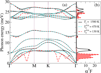
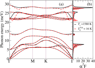
Figure 8 shows non-adiabatic effects on phonon modes in the case of doping for two low temperatures ( = 130 and 470 K) together with a high enough temperature ( = 1580 K). In order to perceive the effect of the phonon softening on , = 130 K is chosen such that it is slightly larger than = 120 K. Employing non-adiabatic phonons at = 130 K for the calculation of results in a slight enhancement of = 57 K within anisotropic Eliashberg theory, which still is much smaller than = 120 K. This lack of enhancement of could be understood based on Allen-Dynes estimation of , as softening related to phonon modes is accompany with shift of to the lower frequencies, = 130 K, in particular in acoustic branches (see Fig.8(b)). This softening results in both remarkable enhancement of and suppression of at the same time which finally leads to a little enhancement of . Notice that the amplitude of the Kohn anomaly decreases in the presence of non-adiabatic effects as one may compare the phonon dispersion corresponding to electronic broadening at K in Figs. 6 and 8.
In addition, the same calculations are repeated for doping and . Applying the non-adiabatic effects on the phonon modes in two cases and at temperatures slightly above their reveal a negligible enhancement of the superconducting transition temperature, = 26, 15 K respectively. This slight enhancement of is simultaneous with a considerable suppression of = 36, 36 K respectively.
Consequently, non-adiabatic effects shift only the CDW region to lower temperatures 120, 191 and 246 K for elevated doping levels and , respectively, and are not capable of suppressing the formation of the CDW instability in these three cases. Therefore, it appears that the superconducting transition for the three mentioned hole doping levels is unlikely to be accessible as a CDW phase forms before a superconductive phase. On the other hand, Table 2 shows no dynamic instability at the remaining doped levels in the presence of non-adiabatic effects.
In Fig. 9 the high temperature phonon dispersion, = 1580 K, and non-adiabatic low temperature one with K are plotted along with their corresponding for hole doping level +0.01. The system is stable even for temperatures considerably smaller than its 54-73 K (see Table 2). Notice that the calculated based on non-adiabatic phonons gives marginally different as small as 2 K, owing to the slight softening at certain q points. Accordingly, the low hole-doped monolayer InSe likely shows a superconductive phase with maximum K. The same analysis holds for hole doping level +0.04, where is far below its as it is shown in Tables 1 and Table 2.
Note that the convergence of Eq. (13) for is carefully checked to adequately explain this equation becomes practically -independent when was changed in the range of 0.0015-0.015 Ry. In addition, the desired results reported in Table 2 show that in the presence of the non-adiabatic effects, monolayer InSe is dynamically stable for all aforesaid doped levels at room temperature because all s are lower than room temperature.
IV Conclusion
In summary, based on the first-principles DFT and DFPT methods, the superconducting properties of pristine monolayer InSe employing the Migdal-Eliashberg theory are explored. We have also calculated the renormalized phonon dispersion owing to the electron-phonon coupling in both the adiabatic and non-adiabatic regimes for various temperatures and doping levels. We have further investigated the competition between CDW formation and the superconductive phase for various hole and electron doping levels.
We have adequately discussed the most important phonon wave vectors leading to the remarkable electron-phonon coupling strength. That correctly expresses the significance of both bare susceptibility and the nesting function below and beyond the Lifshitz transition point. Also, more analyses associated with the polarization of the softened phonon mode at explain that instability at this point mainly involves the in-plane displacements of the In atoms and the out-of-plane displacements of the Se atoms at the same time.
Our desired results show that in some hole-doped cases associated with elevated doping levels beyond the Lifshitz transition point (, and e/f.u.), is much greater than and consequently, CDW instability prevents access to the superconductive phase, whereas, for other hole doping levels, i.e. doping levels below the Lifshitz transition point ( and e/f.u.) and very deep hole doping level e/f.u., is lower than and a maximum K was achieved for low hole doping levels. In the case of very deep hole doping and electron doping, rather small and K, respectively, are obtained. The non-adiabatic phonon effects correctly determining monolayer InSe become dynamically stable for different carrier concentrations at room temperature.
Acknowledgements.
RA was supported by the Australian Research Council Centre of Excellence in Future Low-Energy Electronics Technologies (Project number CE170100039).References
- Novoselov et al. (2004) K. S. Novoselov, A. K. Geim, S. V. Morozov, D. Jiang, Y. Zhang, S. V. Dubonos, I. V. Grigorieva, and A. A. Firsov, “Electric field effect in atomically thin carbon films,” Science 306, 666 (2004).
- Kim et al. (2012) K. K. Kim, A. Hsu, X. Jia, S. M. Kim, Y. Shi, M. Hofmann, D. Nezich, J. F. Rodriguez-Nieva, M. Dresselhaus, T. Palacios, and J. Kong, “Synthesis of monolayer hexagonal boron nitride on cu foil using chemical vapor deposition,” Nano Letters 12, 161 (2012).
- Chhowalla et al. (2013) M. Chhowalla, H. S. Shin, G. Eda, L.-J. Li, K. P. Loh, and H. Zhang, “The chemistry of two-dimensional layered transition metal dichalcogenide nanosheets,” Nature chemistry 5, 263 (2013).
- Huang et al. (2017) B. Huang, G. Clark, E. Navarro-Moratalla, D. R. Klein, R. Cheng, K. L. Seyler, D. Zhong, E. Schmidgall, M. A. McGuire, D. H. Cobden, et al., “Layer-dependent ferromagnetism in a van der Waals crystal down to the monolayer limit,” Nature 546, 270 (2017).
- Li et al. (2014) L. Li, Y. Yu, G. J. Ye, Q. Ge, X. Ou, H. Wu, D. Feng, X. H. Chen, and Y. Zhang, “Black phosphorus field-effect transistors,” Nature nanotechnology 9, 372 (2014).
- Vogt et al. (2012) P. Vogt, P. De Padova, C. Quaresima, J. Avila, E. Frantzeskakis, M. C. Asensio, A. Resta, B. Ealet, and G. Le Lay, “Silicene: Compelling experimental evidence for graphenelike two-dimensional silicon,” Phys. Rev. Lett. 108, 155501 (2012).
- Zólyomi et al. (2013) V. Zólyomi, N. D. Drummond, and V. I. Fal’ko, “Band structure and optical transitions in atomic layers of hexagonal gallium chalcogenides,” Phys. Rev. B 87, 195403 (2013).
- Zólyomi et al. (2014) V. Zólyomi, N. D. Drummond, and V. I. Fal’ko, “Electrons and phonons in single layers of hexagonal indium chalcogenides from ab initio calculations,” Phys. Rev. B 89, 205416 (2014).
- Han et al. (2014) G. Han, Z.-G. Chen, J. Drennan, and J. Zou, “Indium selenides: Structural characteristics, synthesis and their thermoelectric performances,” Small 10, 2747 (2014).
- Lei et al. (2014) S. Lei, L. Ge, S. Najmaei, A. George, R. Kappera, J. Lou, M. Chhowalla, H. Yamaguchi, G. Gupta, R. Vajtai, A. D. Mohite, and P. M. Ajayan, “Evolution of the electronic band structure and efficient photo-detection in atomic layers of inse,” ACS Nano 8, 1263 (2014), pMID: 24392873.
- Politano et al. (2017) A. Politano, D. Campi, M. Cattelan, I. B. Amara, S. Jaziri, A. Mazzotti, A. Barinov, B. Gürbulak, S. Duman, S. Agnoli, et al., “Indium selenide: an insight into electronic band structure and surface excitations,” Scientific reports 7, 3445 (2017).
- Gürbulak et al. (2014) B. Gürbulak, M. Şata, S. Dogan, S. Duman, A. Ashkhasi, and E. F. Keskenler, “Structural characterizations and optical properties of inse and inse:ag semiconductors grown by bridgman/stockbarger technique,” Physica E: Low-dimensional Systems and Nanostructures 64, 106 (2014).
- Julien and Balkanski (2003) C. Julien and M. Balkanski, “Lithium reactivity with iii–vi layered compounds,” Materials Science and Engineering: B 100, 263 (2003).
- Chen (2019) J. Chen, “Phonon-mediated superconductivity in electron-doped monolayer inse: A first-principles investigation,” Journal of Physics and Chemistry of Solids 125, 23 (2019).
- Lugovskoi et al. (2019a) A. V. Lugovskoi, M. I. Katsnelson, and A. N. Rudenko, “Strong electron-phonon coupling and its influence on the transport and optical properties of hole-doped single-layer inse,” Phys. Rev. Lett. 123, 176401 (2019a).
- Mudd et al. (2013) G. W. Mudd, S. A. Svatek, T. Ren, A. Patanè, O. Makarovsky, L. Eaves, P. H. Beton, Z. D. Kovalyuk, G. V. Lashkarev, Z. R. Kudrynskyi, and A. I. Dmitriev, “Tuning the bandgap of exfoliated inse nanosheets by quantum confinement,” Advanced Materials 25, 5714 (2013).
- Mudd et al. (2014) G. W. Mudd, A. Patanè, Z. R. Kudrynskyi, M. W. Fay, O. Makarovsky, L. Eaves, Z. D. Kovalyuk, V. Zólyomi, and V. Falko, “Quantum confined acceptors and donors in inse nanosheets,” Applied Physics Letters 105, 221909 (2014).
- Feng et al. (2015) W. Feng, W. Zheng, X. Chen, G. Liu, and P. Hu, “Gate modulation of threshold voltage instability in multilayer inse field effect transistors,” ACS Applied Materials & Interfaces 7, 26691 (2015), pMID: 26575205.
- Cui et al. (2015) X. Cui, G.-H. Lee, Y. D. Kim, G. Arefe, P. Y. Huang, C.-H. Lee, D. A. Chenet, X. Zhang, L. Wang, F. Ye, et al., “Multi-terminal transport measurements of mos 2 using a van der waals heterostructure device platform,” Nature nanotechnology 10, 534 (2015).
- Sun et al. (2016) C. Sun, H. Xiang, B. Xu, Y. Xia, J. Yin, and Z. Liu, “Ab initio study of carrier mobility of few-layer InSe,” Applied Physics Express 9, 035203 (2016).
- Bandurin et al. (2017) D. A. Bandurin, A. V. Tyurnina, L. Y. Geliang, A. Mishchenko, V. Zólyomi, S. V. Morozov, R. K. Kumar, R. V. Gorbachev, Z. R. Kudrynskyi, S. Pezzini, et al., “High electron mobility, quantum hall effect and anomalous optical response in atomically thin inse,” Nature nanotechnology 12, 223 (2017).
- Marin et al. (2018) E. G. Marin, D. Marian, G. Iannaccone, and G. Fiori, “First-principles simulations of fets based on two-dimensional inse,” IEEE Electron Device Letters 39, 626 (2018).
- Bardeen et al. (1957) J. Bardeen, L. N. Cooper, and J. R. Schrieffer, “Theory of superconductivity,” Phys. Rev. 108, 1175 (1957).
- Cao et al. (2015) T. Cao, Z. Li, and S. G. Louie, “Tunable magnetism and half-metallicity in hole-doped monolayer gase,” Phys. Rev. Lett. 114, 236602 (2015).
- Dresselhaus et al. (2007) M. Dresselhaus, G. Chen, M. Tang, R. Yang, H. Lee, D. Wang, Z. Ren, J.-P. Fleurial, and P. Gogna, “New directions for low-dimensional thermoelectric materials,” Advanced Materials 19, 1043 (2007).
- Hung et al. (2017) N. T. Hung, A. R. T. Nugraha, and R. Saito, “Two-dimensional inse as a potential thermoelectric material,” Applied Physics Letters 111, 092107 (2017).
- Wu et al. (2014) S. Wu, X. Dai, H. Yu, H. Fan, J. Hu, and W. Yao, “Magnetisms in -type monolayer gallium chalcogenides (gase, gas),” arXiv preprint arXiv:1409.4733 (2014).
- Ludbrook et al. (2015) B. M. Ludbrook, G. Levy, P. Nigge, M. Zonno, M. Schneider, D. J. Dvorak, C. N. Veenstra, S. Zhdanovich, D. Wong, P. Dosanjh, C. Straßer, A. Stöhr, S. Forti, C. R. Ast, U. Starke, and A. Damascelli, “Evidence for superconductivity in li-decorated monolayer graphene,” Proceedings of the National Academy of Sciences 112, 11795 (2015).
- Ichinokura et al. (2016) S. Ichinokura, K. Sugawara, A. Takayama, T. Takahashi, and S. Hasegawa, “Superconducting calcium-intercalated bilayer graphene,” ACS Nano 10, 2761 (2016).
- Profeta et al. (2012) G. Profeta, M. Calandra, and F. Mauri, “Phonon-mediated superconductivity in graphene by lithium deposition,” Nature physics 8, 131 (2012).
- Xue et al. (2012) M. Xue, G. Chen, H. Yang, Y. Zhu, D. Wang, J. He, and T. Cao, “Superconductivity in potassium-doped few-layer graphene,” Journal of the American Chemical Society 134, 6536 (2012).
- Baroni et al. (2001) S. Baroni, S. de Gironcoli, A. Dal Corso, and P. Giannozzi, “Phonons and related crystal properties from density-functional perturbation theory,” Rev. Mod. Phys. 73, 515 (2001).
- Calandra et al. (2010) M. Calandra, G. Profeta, and F. Mauri, “Adiabatic and nonadiabatic phonon dispersion in a wannier function approach,” Phys. Rev. B 82, 165111 (2010).
- Lazzeri and Mauri (2006) M. Lazzeri and F. Mauri, “Nonadiabatic kohn anomaly in a doped graphene monolayer,” Phys. Rev. Lett. 97, 266407 (2006).
- Saitta et al. (2008) A. M. Saitta, M. Lazzeri, M. Calandra, and F. Mauri, “Giant nonadiabatic effects in layer metals: Raman spectra of intercalated graphite explained,” Phys. Rev. Lett. 100, 226401 (2008).
- Novko et al. (2019) D. Novko, Q. Zhang, and P. Kaghazchi, “Nonadiabatic effects in raman spectra of alcl4-graphite based batteries,” Phys. Rev. Applied 12, 024016 (2019).
- Giannozzi et al. (2009) P. Giannozzi, S. Baroni, N. Bonini, M. Calandra, R. Car, C. Cavazzoni, D. Ceresoli, G. L. Chiarotti, M. Cococcioni, I. Dabo, A. D. Corso, S. de Gironcoli, S. Fabris, G. Fratesi, R. Gebauer, U. Gerstmann, C. Gougoussis, A. Kokalj, M. Lazzeri, L. Martin-Samos, N. Marzari, F. Mauri, R. Mazzarello, S. Paolini, A. Pasquarello, L. Paulatto, C. Sbraccia, S. Scandolo, G. Sclauzero, A. P. Seitsonen, A. Smogunov, P. Umari, and R. M. Wentzcovitch, “Quantum espresso: a modular and open-source software project for quantum simulations of materials,” Journal of Physics: Condensed Matter 21, 395502 (2009).
- Wierzbowska et al. (2005) M. Wierzbowska, S. de Gironcoli, and P. Giannozzi, “Origins of low-and high-pressure discontinuities of {} in niobium,” arXiv preprint cond-mat/0504077 (2005).
- Marzari and Vanderbilt (1997) N. Marzari and D. Vanderbilt, “Maximally localized generalized wannier functions for composite energy bands,” Phys. Rev. B 56, 12847 (1997).
- Souza et al. (2001) I. Souza, N. Marzari, and D. Vanderbilt, “Maximally localized wannier functions for entangled energy bands,” Phys. Rev. B 65, 035109 (2001).
- Mostofi et al. (2008) A. A. Mostofi, J. R. Yates, Y.-S. Lee, I. Souza, D. Vanderbilt, and N. Marzari, “wannier90: A tool for obtaining maximally-localised wannier functions,” Computer Physics Communications 178, 685 (2008).
- Poncé et al. (2016) S. Poncé, E. Margine, C. Verdi, and F. Giustino, “Epw: Electron–phonon coupling, transport and superconducting properties using maximally localized wannier functions,” Computer Physics Communications 209, 116 (2016).
- Verstraete and Gonze (2001) M. Verstraete and X. Gonze, “Smearing scheme for finite-temperature electronic-structure calculations,” Phys. Rev. B 65, 035111 (2001).
- Albertini et al. (2017) O. R. Albertini, A. Y. Liu, and M. Calandra, “Effect of electron doping on lattice instabilities in single-layer ,” Phys. Rev. B 95, 235121 (2017).
- Kohn (1959) W. Kohn, “Image of the fermi surface in the vibration spectrum of a metal,” Phys. Rev. Lett. 2, 393 (1959).
- Migdal (1958) A. Migdal, “Interaction between electrons and lattice vibrations in a normal metal,” Sov. Phys. JETP 7, 996 (1958).
- Eliashberg (1960) G. Eliashberg, “Interactions between electrons and lattice vibrations in a superconductor,” Sov. Phys. JETP 11, 696 (1960).
- Allen and Dynes (1975) P. B. Allen and R. Dynes, “Transition temperature of strong-coupled superconductors reanalyzed,” Physical Review B 12, 905 (1975).
- Not (a) (a), deformation potential is defined as .
- Margine and Giustino (2013) E. R. Margine and F. Giustino, “Anisotropic migdal-eliashberg theory using wannier functions,” Phys. Rev. B 87, 024505 (2013).
- Not (b) (b), .
- Novko (2020) D. Novko, “Broken adiabaticity induced by lifshitz transition in mos 2 and ws 2 single layers,” Communications Physics 3, 1 (2020).
- Giustino (2017) F. Giustino, “Electron-phonon interactions from first principles,” Rev. Mod. Phys. 89, 015003 (2017).
- Efetov and Kim (2010) D. K. Efetov and P. Kim, “Controlling electron-phonon interactions in graphene at ultrahigh carrier densities,” Phys. Rev. Lett. 105, 256805 (2010).
- Esfahani and Asgari (2017) D. N. Esfahani and R. Asgari, “Superconducting critical temperature of hole doped blue phosphorene,” arXiv preprint arXiv:1710.05554 (2017).
- Lugovskoi et al. (2019b) A. V. Lugovskoi, M. I. Katsnelson, and A. N. Rudenko, “Electron-phonon properties, structural stability, and superconductivity of doped antimonene,” Phys. Rev. B 99, 064513 (2019b).
- Duong et al. (2015) D. L. Duong, M. Burghard, and J. C. Schön, “Ab initio computation of the transition temperature of the charge density wave transition in ,” Phys. Rev. B 92, 245131 (2015).
- Gruner (1994) G. Gruner, Density waves in solids (Perseus, Cambridge, 1994).