Coherent superconducting qubits from a subtractive junction fabrication process
Abstract
Josephson tunnel junctions are the centerpiece of almost any superconducting electronic circuit, including qubits. Typically, the junctions for qubits are fabricated using shadow evaporation techniques to reduce dielectric loss contributions from the superconducting film interfaces. In recent years, however, sub-micron scale overlap junctions have started to attract attention. Compared to shadow mask techniques, neither an angle dependent deposition nor free-standing bridges or overlaps are needed, which are significant limitations for wafer-scale processing. This comes at the cost of breaking the vacuum during fabrication, but simplifies integration in multi-layered circuits, implementation of vastly different junction sizes, and enables fabrication on a larger scale in an industrially-standardized process. In this work, we demonstrate the feasibility of a subtractive process for fabrication of overlap junctions. In an array of test contacts, we find low aging of the average normal state resistance of only 1.6% over 6 months. We evaluate the coherence properties of the junctions by employing them in superconducting transmon qubits. In time domain experiments, we find that both, the qubit life- and coherence time of our best device, are on average greater than . Finally, we discuss potential improvements to our technique. This work paves the way towards a more standardized process flow with advanced materials and growth processes, and constitutes an important step for large scale fabrication of superconducting quantum circuits.
Superconducting qubits are one of the most promising platforms to realize a universal quantum computer. In contrast to other popular qubit implementations, such as trapped ions Cirac and Zoller (1995), cold atoms Bloch (2008), and NV centers Jelezko and Wrachtrup (2006), the properties of superconducting qubits are defined by a micro-fabricated electrical circuit. Consequently, most qubit parameters are adjustable by the circuit design and fabrication, and even the physical encoding of a quantum state is flexible Nakamura, Pashkin, and Tsai (1999); Martinis et al. (2002); Chiorescu et al. (2003); Koch et al. (2007); Manucharyan et al. (2009).
Superconducting qubits feature good coherence times in the range of Paik et al. (2011); Barends et al. (2013); Nersisyan et al. (2019); Place et al. (2020), which is long enough for several hundred to thousand qubit gates Kjaergaard et al. (2020). Most recently, quantum advantage was for the first time demonstrated on a processor consisting of superconducting transmon qubits with an average lifetime of Arute et al. (2019).
The centerpiece of most superconducting qubits are Josephson junctions (JJ) serving as nonlinear elements. Their nonlinearity allows for the isolation of two of the circuit’s quantum levels, usually ground, and first excited state, which may then be used as logical quantum states for computation.
Currently, several different techniques are employed to generate the superconductor-insulator-superconductor interface of the JJ. Most processes rely on electron-beam lithography as smaller areas enable lower loss in the JJ Martinis et al. (2005); Weides et al. (2011a). In the commonly used shadow-evaporation processes, free standing bridges Dolan (1977) or overhangs Lecocq et al. (2011), and multi-angle evaporation are exploited to generate the desired interface in situ. One drawback of these techniques is a systematic angle dependent parameter spread across larger wafers, where great efforts are necessary to mitigate this spread Foroozani et al. (2019); Kreikebaum et al. (2020). The need for point-like evaporation sources limits the applicable materials and growth processes. When polymer masks are employed in favor of hard masks Dolata et al. (2003); Tsioutsios et al. (2020) the superconductor choice is further restricted to metals with low melting temperatures. Additionally, the JJ can suffer from an outgasing of the resist.
An alternative to shadow-mask technology are overlap JJ, which do not rely on angle dependent evaporation, and therefore promise superior scalability. Early implementations of micron sized overlap JJ with superconducting qubits suffered significantly from dielectric loss Steffen et al. (2006); Weides et al. (2011b); Braumüller et al. (2015). More recently, qubits with nanoscaled contacts feature coherence properties competitive with those stemming from shadow-evaporation techniques Wu et al. (2017).
However, current fabrication processes still rely on double resist stacks, and lift-off steps, limiting processing yield and presenting a potential source of contamination during the deposition Pop et al. (2012); Quintana et al. (2014).
In this work, we implement a subtractive process for patterning the JJ, where both electrodes are structured using etching rather than lift-off, allowing for smaller, more coherent contacts. Eliminating the resist from the evaporation chamber opens the door to homogeneous deposition, the addition of reactive gases, and evaporation at elevated temperatures. Consequently, new electrode materials, or epitaxial growth can be explored Fritz et al. (2019). We demonstrate our fabrication platform using Al-AlOx-Al JJ.
Using an array of test contacts, we study aging of the room temperature resistance, which on average increases by only by 1.6% over 6 months. Transmon qubits fabricated with this technique show good coherence properties, where the life-, and coherence times of our best device exceed on average . The process is fully compatible with modern nanofabrication methods, making it an important ingredient for large scale fabrication of superconducting quantum processors.
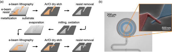
A schematic of the fabrication process is displayed in Fig. 1a.
In the first step, a c-plane sapphire wafer is covered with aluminum at a thickness of , evaporated at a rate of . This layer defines the main structures of the circuit, as well as the bottom electrode of the JJ. Following, the latter is patterned using electron-beam lithography with thick PMMA resist. However, any resist with sufficient resistance to the etching plasma and a satisfactory resolution may be employed. A positive resist reduces electron-beam writing times. Subsequently, the structures are transferred to the aluminum film by reactive ion etching with an Ar/Cl plasma. The plasma is generated inductively using an rf-field with at a gas flow of (sccm) argon and chlorine gas, and is accelerated with a power of . After etching, the remaining resist is removed with a combination of ultrasonic cleaning, acetone, and N-ethyl-pyrrolidone. Milling, oxidation, and deposition of the top electrode are performed in situ, in a PlassysTM MEB550S evaporation machine. First, resist residuals are incinerated in a 30 second Ar/O plasma. The native oxide on the aluminum film is removed by Ar sputtering for 180 seconds Grünhaupt et al. (2017). Immediately afterwards, the AlOx tunnel barrier is grown in a controlled manner by dynamic oxidation for 30 minutes, admitting a continuous flow of O2 to the load lock, at chamber pressure of . The thick aluminum top layer is deposited in vacuum at a rate of . Analogously to the bottom electrode, the top layer is patterned with electron-beam lithography and an Ar/Cl plasma. Finally, larger structures can be applied using optical lithography. We note, that this process leaves us with a stray junction, which was shown to have a negative impact on qubit coherence times Lisenfeld et al. (2019). This effect can be mitigated by employing a bandaging technique, which shorts the dielectric of the stray junction Dunsworth et al. (2017).
Using SEM imaging, we identify a process bias of % towards reduced junction edge width. Most likely, the chlorine introduces an isotropic component of the etching plasma, causing an under-etching and sloped side-walls of the aluminum films, thus reducing the width of the contact electrodes. In room temperature measurements, we find a normal state resistance times area product of across 36 test contacts with varied size, fabricated in the same batch as our qubits. After aging for months this value increased by about 1.6%, see Fig. 2. This indicates clean JJ interfaces Pop et al. (2012). For additional information see supplementary material.
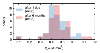
The spread in resistance is similar to that found in shadow evaporated junctions (before meticulous process optimization). It is likely to be caused by the nonuniformity of the electrode edges, constituting % of the total JJ area, due to an isotropic etching component caused by the chlorine. In the future, the spread in normal state resistance can be mitigated by reducing the thickness of both top and bottom electrode, and thereby the duration of the dry etch and effects of under-etching. This also enables the use of thinner electron-beam resists with better resolution. In combination, this allows to decrease overlap area, a crucial step for reducing dielectric loss in the JJ.
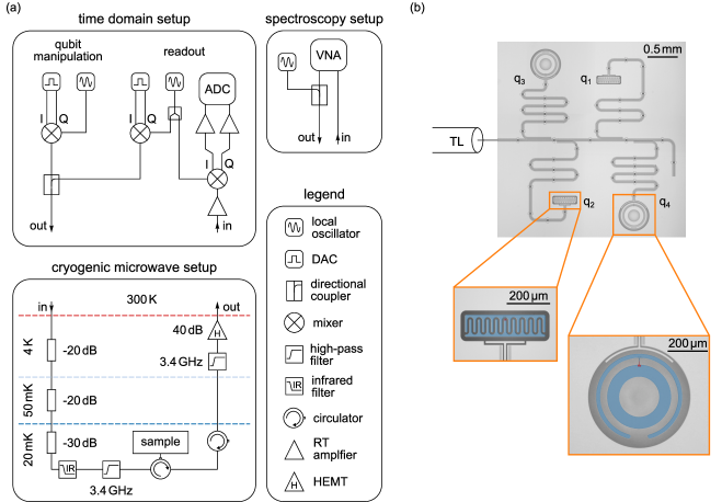
Using the recipe described above, we fabricate a sample comprising two conventional (devices q1 and q2), and two concentric transmon qubitsBraumüller et al. (2016) (devices q3 and q4), embedded in a coplanar microwave environment, see Fig. 1b. A micrograph of the whole chip, our approach in identifying the qubits, and details on the qubit fabrication can be found in the supplementary material. For readout purposes, the qubits are capacitively coupled to a distributed -resonator, which are addressed in reflection measurements. The qubit population is determined by the dispersive shift of the respective readout resonator’s frequency Blais et al. (2004); Wallraff et al. (2004). Table 1 summarizes the essential parameters of all four devices, which were extracted using spectroscopy measurements. The qubit-resonator coupling was calculated from the dispersive shift of the corresponding readout resonator.
| device | |||||
|---|---|---|---|---|---|
| q1 | 6460 | 3548 | 0.915 | ||
| q2 | 6632 | 3950 | 0.514 | ||
| q3 | 6462 | 3161 | 0.350 | ||
| q4 | 6457 | 3324 | 0.774 |
We measure the lifetime , Ramsey decay time , and spin-echo decay time of all qubits over several hours. By employing an interleaved measurement scheme, we resolve slow fluctuations of the qubit frequencies, life-, and coherence times Schlör et al. (2019); Burnett et al. (2019); Hong et al. (2020). For each qubit, the combined measurement of a set of , and takes for point averages. A typical measurement trace from device q4 is displayed in Fig. 3.
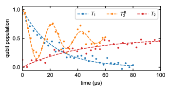
Here, the -pulse in the Ramsey-sequence was detuned by , which results in characteristic oscillations in the laboratory frame of reference. For a detailed sketch of the measurement setup, see supplementary material.
A comparison of the coherence properties of all four qubits is displayed in Fig. 4, in a boxplot. For the full distribution we refer to the supplementary material. Data sets with a fit error exceeding 50% are neglected. Furthermore, we exclude traces where either of the coherence times exceeds , or where . The median lifetime , coherence time , and of all four devices are summarized in table 2.
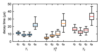
| device | |||
|---|---|---|---|
| q1 | 11.3 | 4.9 | 16.3 |
| q2 | 8.7 | 7.7 | 12.5 |
| q3 | 9.0 | 9.9 | 15.3 |
| q4 | 21.8 | 24.1 | 33.3 |
Devices q1-q3 perform slightly worse than q4. A potential cause is aluminum residuals in the vicinity of the JJ. The performance of device q4 is close to the results of qubits with JJ made from shadow evaporation or lifted overlaps, with state of the art transmon qubits performing better by a factor of . Here, our devices would profit from a reduction of surface loss Gambetta et al. (2017), and optimization of the electrode materials Place et al. (2020).
In conclusion, we established a technique for the subtractive fabrication of coherent JJ. Our recipe does generally not rely on lift-off processes, is angle independent, and tolerates depositions at elevated temperatures and in reactive gases. Furthermore, our approach is extremely flexible with respect to the electrode materials, and growth processes. The junctions feature low aging of the normal state resistance, indicating clean JJ interfaces. These are important ingredients for streamlined and large scale processing platform of superconducting quantum processors. We demonstrated good coherence properties of four transmon qubits with subtractive JJ, where the average life- and coherence times of our best device exceed .
Acknowledgements.
Cleanroom facilities use was supported by the KIT Nanostructure Service Laboratory (NSL). We thank A. Lukashenko for technical support. This work was supported by the European Research Council (ERC) under the Grant Agreement No. 648011, Deutsche Forschungsgemeinschaft (DFG) projects INST 121384/138-1FUGG and WE 4359-7, EPSRC Hub in Quantum Computing and Simulation EP/T001062/1, and the Initiative and Networking Fund of the Helmholtz Association. AS acknowledges support from the Landesgraduiertenförderung Baden-Württemberg (LGF), JDB acknowledges support from the Studienstiftung des Deutschen Volkes. TW acknowledges support from the Helmholtz International Research School for Teratronics (HIRST). AVU acknowledges partial support from the Ministry of Education and Science of the Russian Federation in the framework of the Increase Competitiveness Program of the National University of Science and Technology MISIS (contract No. K2-2020-017).Availability
This article may be downloaded for personal use only. Any other use requires prior permission of the author and AIP Publishing. This article appeared in Stehli et al. (2020) and may be found at https://aip.scitation.org/doi/10.1063/5.0023533. The data that support the findings of this study are available from the corresponding author upon reasonable request.
References
References
- Cirac and Zoller (1995) J. I. Cirac and P. Zoller, “Quantum Computations with Cold Trapped Ions,” Physical Review Letters 74, 4091–4094 (1995).
- Bloch (2008) I. Bloch, “Quantum coherence and entanglement with ultracold atoms in optical lattices,” Nature 453, 1016–1022 (2008).
- Jelezko and Wrachtrup (2006) F. Jelezko and J. Wrachtrup, “Single defect centres in diamond: A review,” physica status solidi (a) 203, 3207–3225 (2006).
- Nakamura, Pashkin, and Tsai (1999) Y. Nakamura, Y. A. Pashkin, and J. S. Tsai, “Coherent control of macroscopic quantum states in a single-Cooper-pair box,” Nature 398, 786–788 (1999).
- Martinis et al. (2002) J. M. Martinis, S. Nam, J. Aumentado, and C. Urbina, “Rabi Oscillations in a Large Josephson-Junction Qubit,” Physical Review Letters 89, 117901 (2002).
- Chiorescu et al. (2003) I. Chiorescu, Y. Nakamura, C. J. P. M. Harmans, and J. E. Mooij, “Coherent Quantum Dynamics of a Superconducting Flux Qubit,” Science 299, 1869–1871 (2003).
- Koch et al. (2007) J. Koch, T. M. Yu, J. Gambetta, A. A. Houck, D. I. Schuster, J. Majer, A. Blais, M. H. Devoret, S. M. Girvin, and R. J. Schoelkopf, “Charge-insensitive qubit design derived from the Cooper pair box,” Physical Review A - Atomic, Molecular, and Optical Physics 76, 42319 (2007).
- Manucharyan et al. (2009) V. E. Manucharyan, J. Koch, L. I. Glazman, and M. H. Devoret, “Fluxonium: Single Cooper-Pair Circuit Free of Charge Offsets,” Science 326, 113–116 (2009).
- Paik et al. (2011) H. Paik, D. I. Schuster, L. S. Bishop, G. Kirchmair, G. Catelani, A. P. Sears, B. R. Johnson, M. J. Reagor, L. Frunzio, L. I. Glazman, S. M. Girvin, M. H. Devoret, and R. J. Schoelkopf, “Observation of high coherence in Josephson junction qubits measured in a three-dimensional circuit QED architecture,” Physical Review Letters 107, 240501 (2011).
- Barends et al. (2013) R. Barends, J. Kelly, A. Megrant, D. Sank, E. Jeffrey, Y. Chen, Y. Yin, B. Chiaro, J. Mutus, C. Neill, P. O’Malley, P. Roushan, J. Wenner, T. C. White, A. N. Cleland, and J. M. Martinis, “Coherent josephson qubit suitable for scalable quantum integrated circuits,” Physical Review Letters 111, 1–5 (2013).
- Nersisyan et al. (2019) A. Nersisyan, E. A. Sete, S. Stanwyck, A. Bestwick, M. Reagor, S. Poletto, N. Alidoust, R. Manenti, R. Renzas, C.-V. Bui, K. Vu, T. Whyland, and Y. Mohan, “Manufacturing low dissipation superconducting quantum processors,” in 2019 IEEE International Electron Devices Meeting (IEDM), Vol. 2019-Decem (IEEE, 2019) pp. 31.1.1–31.1.4.
- Place et al. (2020) A. P. M. Place, L. V. H. Rodgers, P. Mundada, B. M. Smitham, M. Fitzpatrick, Z. Leng, A. Premkumar, J. Bryon, S. Sussman, G. Cheng, T. Madhavan, H. K. Babla, B. Jaeck, A. Gyenis, N. Yao, R. J. Cava, N. P. de Leon, and A. A. Houck, “New material platform for superconducting transmon qubits with coherence times exceeding 0.3 milliseconds,” (2020), arXiv:2003.00024 .
- Kjaergaard et al. (2020) M. Kjaergaard, M. E. Schwartz, J. Braumüller, P. Krantz, J. I.-J. Wang, S. Gustavsson, and W. D. Oliver, “Superconducting Qubits: Current State of Play,” Annual Review of Condensed Matter Physics 11, 369–395 (2020).
- Arute et al. (2019) F. Arute, K. Arya, R. Babbush, D. Bacon, J. C. Bardin, R. Barends, R. Biswas, S. Boixo, F. G. Brandao, D. A. Buell, B. Burkett, Y. Chen, Z. Chen, B. Chiaro, R. Collins, W. Courtney, A. Dunsworth, E. Farhi, B. Foxen, A. Fowler, C. Gidney, M. Giustina, R. Graff, K. Guerin, S. Habegger, M. P. Harrigan, M. J. Hartmann, A. Ho, M. Hoffmann, T. Huang, T. S. Humble, S. V. Isakov, E. Jeffrey, Z. Jiang, D. Kafri, K. Kechedzhi, J. Kelly, P. V. Klimov, S. Knysh, A. Korotkov, F. Kostritsa, D. Landhuis, M. Lindmark, E. Lucero, D. Lyakh, S. Mandrà, J. R. McClean, M. McEwen, A. Megrant, X. Mi, K. Michielsen, M. Mohseni, J. Mutus, O. Naaman, M. Neeley, C. Neill, M. Y. Niu, E. Ostby, A. Petukhov, J. C. Platt, C. Quintana, E. G. Rieffel, P. Roushan, N. C. Rubin, D. Sank, K. J. Satzinger, V. Smelyanskiy, K. J. Sung, M. D. Trevithick, A. Vainsencher, B. Villalonga, T. White, Z. J. Yao, P. Yeh, A. Zalcman, H. Neven, and J. M. Martinis, “Quantum supremacy using a programmable superconducting processor,” Nature 574, 505–510 (2019).
- Martinis et al. (2005) J. M. Martinis, K. B. Cooper, R. McDermott, M. Steffen, M. Ansmann, K. D. Osborn, K. Cicak, S. Oh, D. P. Pappas, R. W. Simmonds, and C. C. Yu, “Decoherence in Josephson Qubits from Dielectric Loss,” Physical Review Letters 95, 210503 (2005).
- Weides et al. (2011a) M. Weides, R. C. Bialczak, M. Lenander, E. Lucero, M. Mariantoni, M. Neeley, A. D. O’Connell, D. Sank, H. Wang, J. Wenner, T. Yamamoto, Y. Yin, A. N. Cleland, and J. Martinis, “Phase qubits fabricated with trilayer junctions,” Superconductor Science and Technology 24, 055005 (2011a).
- Dolan (1977) G. J. Dolan, “Offset masks for lift-off photoprocessing,” Applied Physics Letters 31, 337–339 (1977).
- Lecocq et al. (2011) F. Lecocq, I. M. Pop, Z. Peng, I. Matei, T. Crozes, T. Fournier, C. Naud, W. Guichard, and O. Buisson, “Junction fabrication by shadow evaporation without a suspended bridge,” Nanotechnology 22, 315302 (2011).
- Foroozani et al. (2019) N. Foroozani, C. Hobbs, C. C. Hung, S. Olson, D. Ashworth, E. Holland, M. Malloy, P. Kearney, B. O’Brien, B. Bunday, D. DiPaola, W. Advocate, T. Murray, P. Hansen, S. Novak, S. Bennett, M. Rodgers, B. Baker-O’Neal, B. Sapp, E. Barth, J. Hedrick, R. Goldblatt, S. S. P. Rao, and K. D. Osborn, “Development of transmon qubits solely from optical lithography on 300 mm wafers,” Quantum Science and Technology 4, 025012 (2019).
- Kreikebaum et al. (2020) J. M. Kreikebaum, K. P. O’Brien, A. Morvan, and I. Siddiqi, “Improving wafer-scale Josephson junction resistance variation in superconducting quantum coherent circuits,” Superconductor Science and Technology 33, 06LT02 (2020).
- Dolata et al. (2003) R. Dolata, H. Scherer, A. B. Zorin, and J. Niemeyer, “Single electron transistors with Nb/AlO[sub x]/Nb junctions,” Journal of Vacuum Science & Technology B: Microelectronics and Nanometer Structures 21, 775 (2003).
- Tsioutsios et al. (2020) I. Tsioutsios, K. Serniak, S. Diamond, V. V. Sivak, Z. Wang, S. Shankar, L. Frunzio, R. J. Schoelkopf, and M. H. Devoret, “Free-standing silicon shadow masks for transmon qubit fabrication,” AIP Advances 10, 065120 (2020).
- Steffen et al. (2006) M. Steffen, M. Ansmann, R. McDermott, N. Katz, R. C. Bialczak, E. Lucero, M. Neeley, E. M. Weig, A. N. Cleland, and J. M. Martinis, “State Tomography of Capacitively Shunted Phase Qubits with High Fidelity,” Physical Review Letters 97, 050502 (2006).
- Weides et al. (2011b) M. P. Weides, J. S. Kline, M. R. Vissers, M. O. Sandberg, D. S. Wisbey, B. R. Johnson, T. A. Ohki, and D. P. Pappas, “Coherence in a transmon qubit with epitaxial tunnel junctions,” Applied Physics Letters 99, 262502 (2011b).
- Braumüller et al. (2015) J. Braumüller, J. Cramer, S. Schlör, H. Rotzinger, L. Radtke, A. Lukashenko, P. Yang, S. T. Skacel, S. Probst, M. Marthaler, L. Guo, A. V. Ustinov, and M. Weides, “Multiphoton dressing of an anharmonic superconducting many-level quantum circuit,” Physical Review B 91, 54523 (2015).
- Wu et al. (2017) X. Wu, J. L. Long, H. S. Ku, R. E. Lake, M. Bal, and D. P. Pappas, “Overlap junctions for high coherence superconducting qubits,” Applied Physics Letters 111, 032602 (2017).
- Pop et al. (2012) I. M. Pop, T. Fournier, T. Crozes, F. Lecocq, I. Matei, B. Pannetier, O. Buisson, and W. Guichard, “Fabrication of stable and reproducible submicron tunnel junctions,” Journal of Vacuum Science & Technology B, Nanotechnology and Microelectronics: Materials, Processing, Measurement, and Phenomena 30, 010607 (2012).
- Quintana et al. (2014) C. M. Quintana, A. Megrant, Z. Chen, A. Dunsworth, B. Chiaro, R. Barends, B. Campbell, Y. Chen, I.-C. Hoi, E. Jeffrey, J. Kelly, J. Y. Mutus, P. J. J. O’Malley, C. Neill, P. Roushan, D. Sank, A. Vainsencher, J. Wenner, T. C. White, A. N. Cleland, and J. M. Martinis, “Characterization and reduction of microfabrication-induced decoherence in superconducting quantum circuits,” Applied Physics Letters 105, 062601 (2014).
- Fritz et al. (2019) S. Fritz, L. Radtke, R. Schneider, M. Luysberg, M. Weides, and D. Gerthsen, “Structural and nanochemical properties of AlOx layers in Al-AlOx-Al-layer systems for Josephson junctions,” Physical Review Materials 3, 114805 (2019).
- Grünhaupt et al. (2017) L. Grünhaupt, U. Von Lüpke, D. Gusenkova, S. T. Skacel, N. Maleeva, S. Schlör, A. Bilmes, H. Rotzinger, A. V. Ustinov, M. Weides, and I. M. Pop, “An argon ion beam milling process for native AlOx layers enabling coherent superconducting contacts,” Applied Physics Letters 111, 072601 (2017).
- Lisenfeld et al. (2019) J. Lisenfeld, A. Bilmes, A. Megrant, R. Barends, J. Kelly, P. Klimov, G. Weiss, J. M. Martinis, and A. V. Ustinov, “Electric field spectroscopy of material defects in transmon qubits,” npj Quantum Information 5, 105 (2019).
- Dunsworth et al. (2017) A. Dunsworth, A. Megrant, C. Quintana, Z. Chen, R. Barends, B. Burkett, B. Foxen, Y. Chen, B. Chiaro, A. Fowler, R. Graff, E. Jeffrey, J. Kelly, E. Lucero, J. Y. Mutus, M. Neeley, C. Neill, P. Roushan, D. Sank, A. Vainsencher, J. Wenner, T. C. White, and J. M. Martinis, “Characterization and reduction of capacitive loss induced by sub-micron Josephson junction fabrication in superconducting qubits,” Applied Physics Letters 111, 022601 (2017).
- Braumüller et al. (2016) J. Braumüller, M. Sandberg, M. R. Vissers, A. Schneider, S. Schlör, L. Grünhaupt, H. Rotzinger, M. Marthaler, A. Lukashenko, A. Dieter, A. V. Ustinov, M. Weides, and D. P. Pappas, “Concentric transmon qubit featuring fast tunability and an anisotropic magnetic dipole moment,” Applied Physics Letters 108 (2016), 10.1063/1.4940230.
- Blais et al. (2004) A. Blais, R. S. Huang, A. Wallraff, S. M. Girvin, and R. J. Schoelkopf, “Cavity quantum electrodynamics for superconducting electrical circuits: An architecture for quantum computation,” Physical Review A - Atomic, Molecular, and Optical Physics 69, 62320 (2004).
- Wallraff et al. (2004) A. Wallraff, D. I. Schuster, A. Blais, L. Frunzio, R.-S. Huang, J. Majer, S. Kumar, S. M. Girvin, and R. J. Schoelkopf, “Strong coupling of a single photon to a superconducting qubit using circuit quantum electrodynamics,” Nature 431, 162–167 (2004).
- Schlör et al. (2019) S. Schlör, J. Lisenfeld, C. Müller, A. Bilmes, A. Schneider, D. P. Pappas, A. V. Ustinov, and M. Weides, “Correlating Decoherence in Transmon Qubits: Low Frequency Noise by Single Fluctuators,” Physical Review Letters 123, 190502 (2019).
- Burnett et al. (2019) J. J. Burnett, A. Bengtsson, M. Scigliuzzo, D. Niepce, M. Kudra, P. Delsing, and J. Bylander, “Decoherence benchmarking of superconducting qubits,” npj Quantum Information 5, 54 (2019).
- Hong et al. (2020) S. S. Hong, A. T. Papageorge, P. Sivarajah, G. Crossman, N. Didier, A. M. Polloreno, E. A. Sete, S. W. Turkowski, M. P. Da Silva, and B. R. Johnson, “Demonstration of a parametrically activated entangling gate protected from flux noise,” Physical Review A 101, 1–8 (2020).
- Gambetta et al. (2017) J. M. Gambetta, C. E. Murray, Y.-K.-K. Fung, D. T. McClure, O. Dial, W. Shanks, J. W. Sleight, and M. Steffen, “Investigating Surface Loss Effects in Superconducting Transmon Qubits,” IEEE Transactions on Applied Superconductivity 27, 1–5 (2017).
- Stehli et al. (2020) A. Stehli, J. D. Brehm, T. Wolz, P. Baity, S. Danilin, V. Seferai, H. Rotzinger, A. V. Ustinov, and M. Weides, “Coherent superconducting qubits from a subtractive junction fabrication process,” Applied Physics Letters 117, 124005 (2020).
Supplementary material
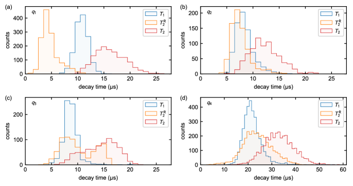
Qubit life-, and coherence time distribution
The distributions of all qubits’ life-, and coherence times are displayed in Fig. S1. As described in the main text, data sets with a fitting error exceeding 50% are excluded. Finally, we also exclude unphysical data sets, i.e., where , , or , which may occur due to fit errors or qubit fluctuations during the measurement. For each qubit table S3 summarizes the number of total, and successful measurements (converged fit), as well as the duration of the measurements.
| device | measurement duration (h) | ||
|---|---|---|---|
| q1 | 29.8 | 1700 | 1589 |
| q2 | 17.6 | 2000 | 1382 |
| q3 | 35.3 | 2502 | 1744 |
| q4 | 69.6 | 10337 | 7013 |
Microwave setup
In Fig. S2a the microwave setup for spectroscopy and time domain experiments, as well as the wiring inside the cryostat, are summarized. In our time domain experiments, we employ single-sideband mixing to generate the desired pulses for qubit manipulation and readout. We use the same local oscillator for up and down conversion of the readout signal. The signal is digitized at a rate of 500 MS/s by an ADC card installed in our measurement PC.
As is common practice, we use a combination of attenuators on various temperature stages, high-pass filter, infrared filters and circulators/isolators to protect the sample form external radiation.
Figure S2b gives an overview of the on-chip microwave setup. Each qubit is coupled capacitively to a dedicated -readout resonator. The resonators couple inductively to a transmission line, which connects to the output of the sample holder on one end, and is terminated to ground on the other.
Normal state JJ resistance and aging
In room temperature measurements we characterize a set of 36 JJ fabricated in the same batch as the qubits. We measure the normal state resistance in a 2-point measurement. Compared to a 4-point probe method the systematic error acquired is negligible due to the large resistance () of the contacts. For better comparability, we multiply the normal state resistance with the area of the overlap. Immediately after the fabrication, our measurements yield . In order to quantify JJ aging, we repeat the characterization after months. During this time, the samples were stored under ambient conditions. Neglecting measurement inaccuracies, we find a slight increase of about 1.6% to .
Qubit fabrication
In our qubit fabrication, the top electrode is deposited only in a small window above the JJ. Here, an optical lift-off process with S1805 resist was employed. We want to emphasize, that this lift-off step is not process relevant, and has the sole purpose of reducing the electron-beam exposure time. Using a negative tone resist, as done for some of our latest samples, renders it obsolete. The main structures of the qubit sample are also patterned optically, using S1805 resist and an Ar/Cl plasma. We admit an additional flow of of oxygen, which improves the edge roughness of our main structures. During the last process step, the JJ is protected by photo resist.
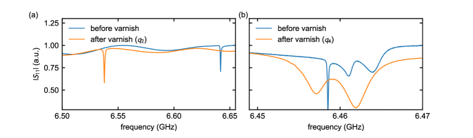
Resonator identification
Due to the close proximity of the readout resonators in frequency space, an identification of the qubits proves challenging. On a dummy chip with the same structures, we applied a drop of varnish on a readout resonator, shifting its transition frequency. Consequently, we can determine which qubit corresponds to the coated resonator. By repeating this process twice we identified two resonator-qubit pairs, see Fig. S3. The identity of the remaining qubits was inferred from their anharmonicity.