Aharonov-Bohm interference as a probe of Majorana fermions
Abstract
Majorana fermions act as their own antiparticle, and they have long been thought to be confined to the realm of pure theory. However, interest in them has recently resurfaced, as it was realized through the work of Kitaev that some experimentally accessible condensed matter systems can host these exotic excitations as bound states on the boundaries of 1D chains, and that their topological and non-abelian nature holds promise for quantum computation. Unambiguously detecting the experimental signatures of Majorana bound states has turned out to be challenging, as many other phenomena lead to similar experimental behaviour. Here, we computationally study a ring comprised of two Kitaev model chains with tunnel coupling between them, where an applied magnetic field allows for Aharonov-Bohm interference in transport through the resulting ring structure. We use a non-equilibrium Green’s function technique to analyse the transport properties of the ring in both the presence and absence of Majorana zero modes. Further, we show that these results are robust against weak disorder in the presence of an applied magnetic field. This computational model suggests another signature for the presence of these topologically protected bound states can be found in the magnetic field dependence of devices with loop geometries.
I Introduction
Majorana fermions were postulated as fermionic excitations that act as their own antiparticle in 1937 Majorana and Maiani (2006), but so far they have not been experimentally shown to exist in nature. More recently it was shown theoretically that 1D systems exhibiting -wave superconductivity within certain parameters host Majorana zero modes (MZMs) at their boundaries Kitaev (2001). It was soon realized that the topological nature of these bound states make them ideal candidates for quantum computation, as it helps to protect them from some types of decoherence Alicea et al. (2011); Lian et al. (2018). Destroying information encoded in this way requires a global perturbation that is strong enough to break the topologically non-trivial phase of the system Ivanov (2001); Volovik (1999). Further, their non-abelian character Kitaev (2001); Read and Green (2000) allows one to manipulate pairs of MZMs through braided exchange of their relative positions, showing a way towards topologically protected quantum computation van Heck et al. (2012); Kitaev (2001); Alicea et al. (2011); Kauffman (2016); Kitaev (2003). One possible experimental system hosting MZMs are one-dimensional (1D) semiconductor wires with strong spin-orbit coupling and proximity induced superconductivity Kitaev (2001); Mourik et al. (2012). Several recent works have reported experimental evidence for the existence of MZMs in such condensed matter systems Zhang et al. (2018a); Mourik et al. (2012); Law et al. (2009); Das et al. (2012); Deng et al. (2012); Rokhinson et al. (2012); Deng et al. (2016). However there exist a number of confounding effects that have signatures similar to MZMs Liu et al. (2018, 2017); Deng et al. (2016); Moore et al. (2018a); Deng et al. (2018); Chiu and Das Sarma (2019); Liu et al. (2018); Moore et al. (2018b) and which make the unambiguous detection of Majorana fermions an ongoing challenge.
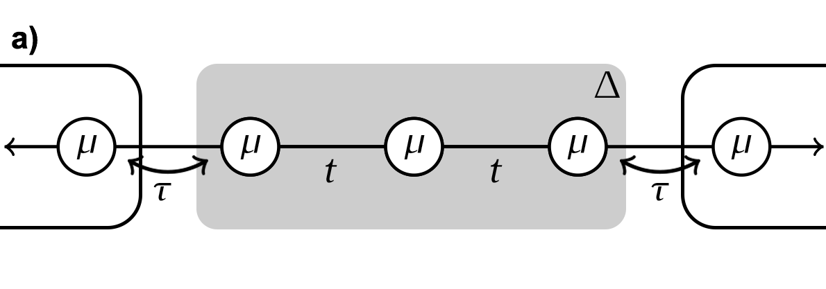
The standard theory model that allows for MZMs is the Kitaev model nanowire Kitaev (2001). It consists of a 1D tight binding chain with proximity induced -wave superconductivity, as illustrated in Fig. 1a. Several different materials have been considered to realise such wires Kitaev (2001); Zhang et al. (2018a); Mourik et al. (2012); Law et al. (2009); Das et al. (2012); Deng et al. (2012); Rokhinson et al. (2012); Deng et al. (2016). Although the system parameters vary between the different materials, for all these systems the key physics can be approximated by the effective Kitaev nanowire Hamiltonian.
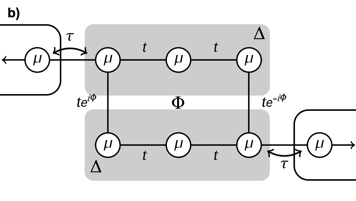
The parameter regimes of the Kitaev nanowire have been extensively studied Kitaev (2001); Chen et al. (2014); Alicea (2012); Lee et al. (2014), as have its transport properties Doornenbal et al. (2015); Weithofer et al. (2014); Danon et al. (2020). By coupling two Kitaev nanowires through non-superconducting links at their ends, we form an Aharonov-Bohm (AB) ring, as illustrated in Fig. 1b.
Different ring geometries have previously been investigated using interferometry where it was suggested the periodicity of the conductance as a function of magnetic field might be used as a way to identify Majorana bound states van Heck et al. (2011); Zeng et al. (2017); Akhmerov et al. (2011); Whiticar et al. (2020). Other studies employed either scattering matrix theory or Green’s function techniques to study a normal AB ring containing a single nanowire hosting MZMs Tripathi et al. (2016); Shang et al. (2014); Benjamin and Pachos (2010); Hansen et al. (2016); Jiang and Zheng (2015). For example, the transport properties of such an AB ring were found to be sensitive to the difference between MZMs and Andreev bound states Tripathi et al. (2016); Haug et al. (2019a, b, c); Qin et al. (2019); Val’kov et al. (2019); Aksenov and Kagan (2020). Studies of two-dimensional systems of finite extent have investigated interference effects due to chiral Majorana fermion edge states at the normal-superconductor boundary Park et al. (2014); Fu and Kane (2009); Law et al. (2009).
In this paper we study the interplay between the AB effect and MZMs, and expand on these previous works by analysing the transport characteristics of an AB ring formed by two coupled Kitaev nanowires. We employ the non-equilibrium Green’s function (NEGF) formalism and explore the relationship between model parameters and transport characteristics for a finite size ring geometry. Previous studies have investigated the case of MZMs in a finite nanowire Zvyagin (2015); Leumer et al. (2020). Such models are particularly useful as all experimentally realizable devices are finite, which limits what can be understood simply from the bulk properties of the materials hosting MZMs. The relation between AB interference and Majorana bound states in such a loop geometry has previously been studied using a scattering matrix approach with the wide-band approximation Zhang et al. (2018b). However energy resolved transport characteristics of such a circuit provide important clues on how such effects can be probed experimentally and will help to further understand the experimental signatures of these topologically non-trivial bound states. Here we show that mapping the energy resolved transmission through an AB ring comprised of two MZMs displays the expected resonance at zero energy. However, mapping this resonance as a function of magnetic field, on-site potential or superconducting order parameter results in characteristic responses, suggesting the possibility of unambiguously distinguishing MZM from trivial bound states.
The paper proceeds as follows: Section II introduces the standard toy model for the Kitaev nanowire. The NEGF formalism is then outlined in Section II.1. Section III expands on the Kitaev nanowire by introducing an AB ring comprised of two coupled Kitaev nanowires. Finally, Section IV examines the transport properties of this ring in the presence of an applied magnetic field. We conclude in Section VI.
| Regime | Model parameters |
|---|---|
| Topologically trivial | |
| Topologically non-trivial | , |
| Superconducting | |
| Normal |
II The Kitaev nanowire
We begin by following Kitaev in defining a model Hamiltonian () for a system admitting the existence of MZMs as
| (1) |
where is the nearest-neighbour hopping strength, is the on-site potential, is the -wave pairing amplitude, is the superconducting phase and N is the number of sites in the chain. Without loss of generality we set where , resulting in . is the fermionic annihilation operator acting on the site. We write a particle-hole symmetric (PHS) form of the Hamiltonian through the Bogoliubov-deGennes (BdG) Hamiltonian:
| (2) |
is the Hamiltonian for a normal wire and is the -wave pairing amplitude between particles and holes. For more details see App. A. Following Chen et al.Chen et al. (2014) we model the Kitaev nanowire as a 1D tight binding chain that consists of 50 sites with the on-site potential and -wave pairing amplitude as adjustable parameters. The essential physics studied here remains unchanged with the length of the chain, so long as the chain is long enough such that the groundstate wavefunctions do not overlap, as is the requirement for topologically non-trivial MZMs. To calculate the electrical response of the 1D Kitaev nanowire we couple it to normal leads on either side and apply an NEGF technique, as is described in Sec. II.1.
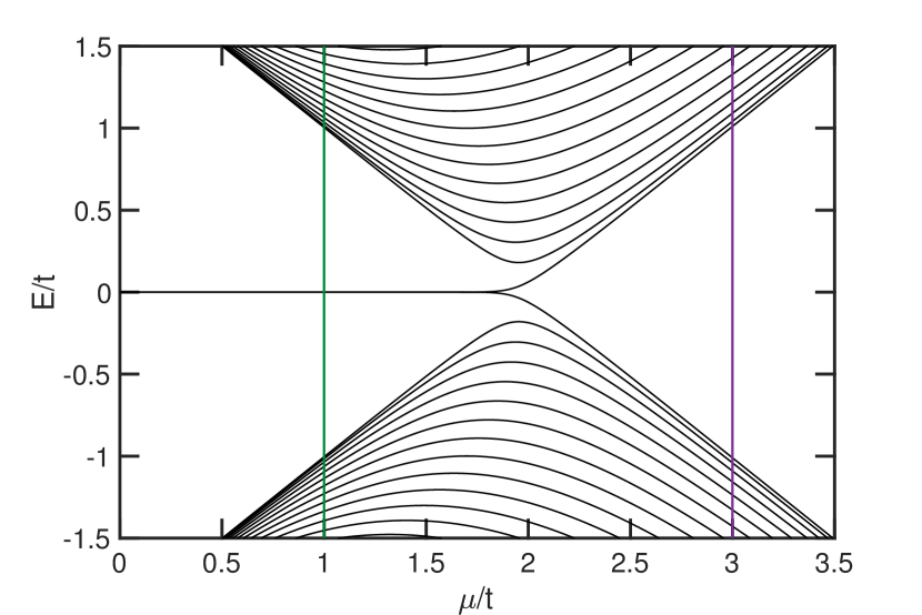
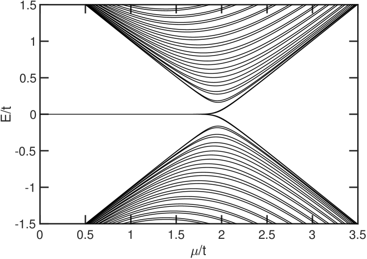
The Kitaev Hamiltonian has three different regimes which are of interest to us here, these are the topologically trivial, the topologically non-trivial, and the superconducting regime. The different model parameters for each of these regimes are summarized in Tab. 1, where we also list parameters for the normal (non-superconducting) regime. Fig. 2 shows how the eigenspectrum of this Hamiltonian depends on the value of . In this figure we see the separation of the topologically trivial and non-trivial regimes at approximately . When the system is topologically non-trivial and we have a degenerate ground state at . In the topologically trivial regime, when , the ground state of the system is no longer degenerate, nor does it appear at .
II.1 Non-equilibrium Green’s function formalism
To calculate the electrical response of a Kitaev nanowire we apply the NEGF formalism Datta (2005), which allows us to compute transmission probabilities as a function of energy. We are also thereby able to introduce open boundary conditions and model transport through the device with changing magnetic field. The retarded Green’s function for the device , from which the transport properties of the system can be calculated, is written as
| (3) |
where is energy and is a small positive number. For brevity we suppress the energy dependence in subsequent Green’s functions, transmission functions, and other operators. The Hamiltonian describing the device is modified by two self-energy terms and to include the left and right leads respectively. These self-energy terms are calculated from the hopping parameter and onsite potential for the leads and are used to model the open boundaries. The nearest-neighbour hopping strength between the leads and the device is given by . These weak links () at the interfaces, together with the self-energy terms, modify the system’s density of states such that resonant tunneling dominates transport through the device. The Green’s function is used along with the Caroli formula (Eq. (4)) to calculate transmission probabilities for particles/holes moving through the device. When applying the NEGF formalism to a conventional charge transport problem, the transmission probability is given by
| (4) |
with and broadening matrices given by
| (5) |
with an index describing the left (L) and right (R) contacts.
The conductance can be calculated viaLundstrom (2000)
| (6) |
where is Planck’s constant, is the charge of the particle, and is the equilibrium Fermi-Dirac distribution function. In the limit as temperature goes to zero, the conductance is simply proportional to the transmission function and therefore in everything that follows we only consider . In general if a voltage bias is applied to the device then the onsite potential becomes spatially dependent and the integral in Eq. 6 must be taken over a range of energies. Although these complications are important in discussing real devices they don’t change the underlying physics and so we focus on the zero bias limit. For the BdG Hamiltonian we must now account for both electron and hole degrees of freedom. We can compute the total transmission probability as the sum of the transmission probabilities for direct transmission , Andreev reflection , and crossed Andreev reflection :
| (7) |
with
| (8) | ||||
| (9) | ||||
| (10) |
Eq. (7) therefore gives the transmission probability of a particle (hole) through the device at a particular energy (see App. B for further details). The broadening matrices are now represented as a matrix due to PHS:
| (11) |
where the superscript represents the type of particles involved in the interaction. For example (e) is a electron-electron interaction and (h) is a hole-hole interaction. As the system has normal leads we do not consider the off-diagonal terms which correspond to electron-hole interaction in the broadening matrices, i.e. . As we are ultimately interested in the total conductance through the device, in what follows we often plot the combined transmission due to electrons and holes, , where the individual electron and hole transmission functions are given by Eq. 7.
II.2 Signatures of Majorana fermions and the zero bias anomaly
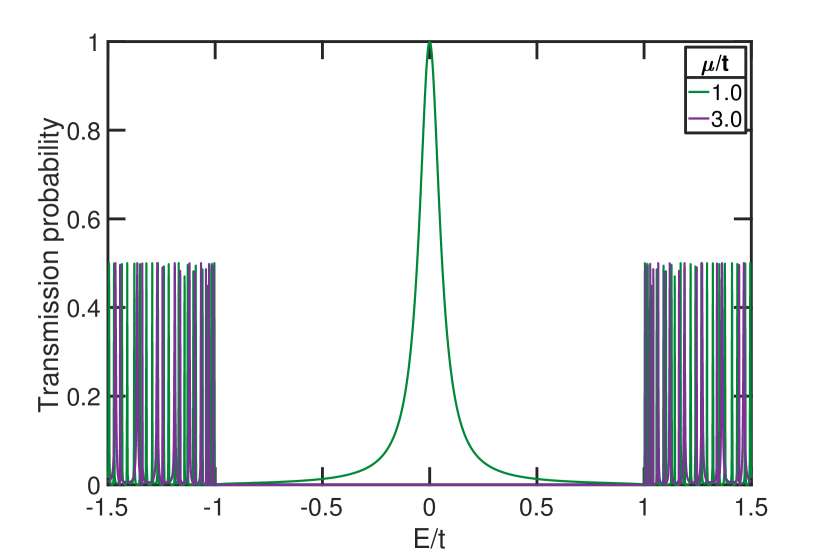
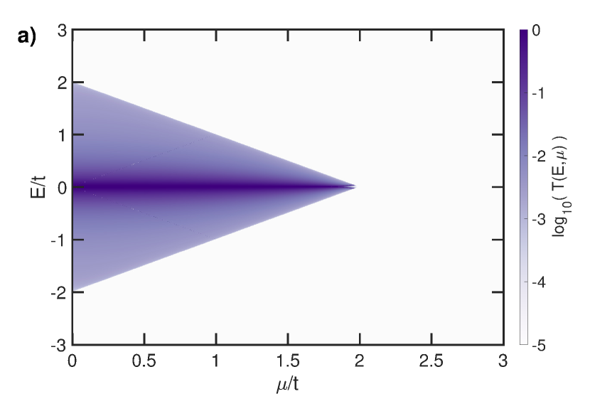
A signature of MZMs in the electrical response of these systems is the existence of a zero-bias anomaly (ZBA) that is topologically protected Das et al. (2012). This ZBA is a conduction mode at that results from the zero-energy ground state of the MZMs. Fig. 3 shows the transmission probability for the 1D Kitaev nanowire in the topologically trivial and the topologically non-trivial regime. The figure shows the transmission probability for a particle through the Kitaev nanowire at , with on-site potentials (, topologically non-trivial) and (, topologically trivial). The presence of a non-zero probability for transmission of a particle at when is characteristic of the ZBAMourik et al. (2012). Here the width of the zero energy peak in the transmission probability is directly related to the strength of the coupling to the device, . As increases there is a stronger connection between the device and the leads, which creates a broader resonance peakDatta (2005). In the topologically trivial regime () there is no zero energy peak as all states of the Hamiltonian fall outside of the energy gap, as seen in Fig. 3.
III The Aharonov-Bohm ring
We now consider a device comprised of two 1D Kitaev nanowires, as illustrated in Fig. 1. This system is capable of supporting two pairs of MZMs (one MZM at each of the four interfaces between the device and the leads). For all AB ring devices modelled here we use a ring comprised of two Kitaev nanowires with 50 sites,
| (12) |
where the off-diagonal blocks are the adjacency matrices defined such that they couple the BdG Hamiltonians at the edges of the wires, as per Fig. 1b and is the Peierls phase for an applied magnetic field.
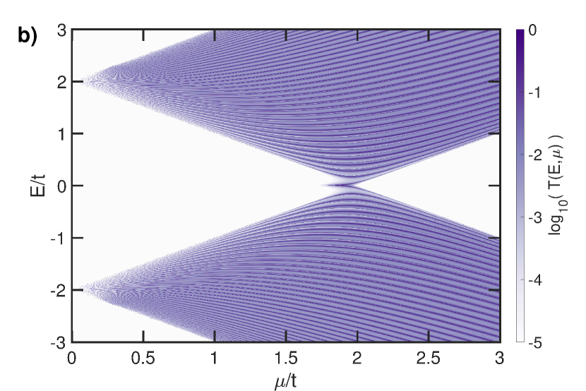
The topological phase diagram for this AB ring is equivalent to the topological phase diagram of the 1D Kitaev nanowire. The presence of a ZBA for the AB ring can been seen in Fig. 4 for each of the parameter regimes described in Tab. 1. The two Kitaev nanowires of the ring are connected by a nearest-neighbour hopping strength of , as shown in Fig. 1b. In all that follows we set . The -wave pairing amplitude between the two nanowires is zero. This corresponds to the case of normal tunneling between two superconducting nanowires.
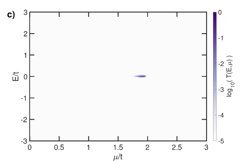
We now apply our NEGF method to an AB ring. Fig. 5 shows the transmission probability for an AB ring at energies close to and values of the on-site potential . For we see peaks form due to the topologically trivial quasi-particle states which lie outside the superconducting energy gap. As is decreased, we see the formation of a peak in the transmission probability at zero energy. The appearance of the ZBA correlates with the system becoming topologically non-trivial. At the zero energy transmission is maximised which suggests that at this value of the on-site potential the system is in the topologically non-trivial regime. The value of at which the system becomes topologically non-trivial is affected by the number of sites. As the number of sites increases the system approaches the ideal case and the value tends to . For relatively small numbers of sites, the value of corresponding to a topological phase transition is reduced due to finite size effects.
By examining each of the individual components of Eq. (7) (given in Eq.(8)-(10)) we are able to see how each component of the transmission probability influences the total transmission probability through the device. It also allows for insight into how the magnetic field induced interference affects each of the difference types of transmission (direct, Andreev and crossed Andreev). Fig. 6 shows the transmission probability as a function of energy and on-site potential for Andreev transmission, direct transmission, and crossed Andreev transmission with a magnetic flux through the ring of . We see in Fig. 6a the sub-gap states are due entirely to resonant Andreev transmission, while in Fig. 6b we see that direct transmission occurs via states above and below the gap. Fig. 6c shows that the crossed Andreev transmission only exists close to the point of transition between trivial and non-trivial topological behaviour, at zero energy and . The crossed Andreev transmission is relatively weak compared to the other contributions.
IV Magnetic field applied to an Aharonov-Bohm ring
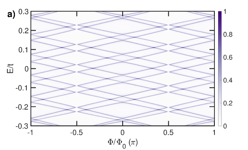
We now apply a perpendicular magnetic field to the AB ring by Peierls substitution to observe interference in the transmission probability Peierls (1933); Maśka and Mierzejewski (2001); Hofstadter (1976). We choose a gauge such that the Peierls phase (equivalent to magnetic flux through the ring and given here in units of flux quanta ) drops across only the normal links. By applying a magnetic field to the AB ring in the topologically trivial and non-trivial regimes, we see the changes in the transmission probability as a function of magnetic flux due to the presence (or absence) of the MZMs.
Resonances in the transport spectrum of the ring are caused by weak links between the device and the leads Doornenbal et al. (2015). Applying a magnetic field to the AB ring in the normal regime (, ), as in Fig. 7a, we see there is completely destructive interference at , which results in the transmission probability going to zero at these values of magnetic flux. The symmetry of the transmission resonances in Fig. 7 about zero energy follows directly from the PHS. One important consideration is whether such a system would destroy superconductivity in the ring by applying a magnetic field larger than the critical field. To investigate this we can consider a ring of niobium titanium nitride as an example. If the ring has an area of 1 m2, one magnetic flux quanta corresponds to 2 mT, which is considerably smaller than a typical critical field of approximately 28 mT. This would allow the mapping of AB interference for many oscillation periods without collapsing the superconducting stateBosland et al. (1992); Di Leo et al. (1990).
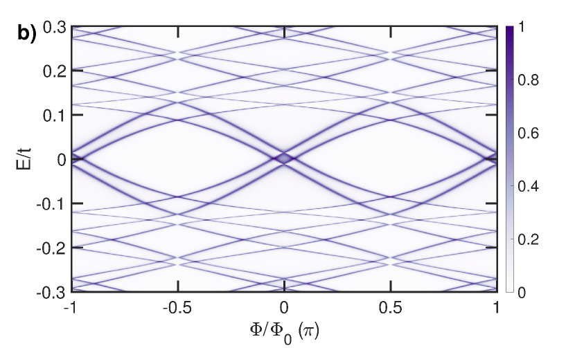
In the case where and , as in Fig. 7b, we see the formation of a sub-gap state that oscillates in energy, as a function of magnetic flux, with a period of . Note that the value of is not large enough to overcome finite size effects here and that the transport spectrum is characterised by a lack of the zero energy state at . Furthermore for a magnetic flux through the ring of there still exists channels available for the conduction of electrons through the device which implies the interference is only partially destructive. This is in contrast to the case of the normal ring (shown in Fig. 7a) where transmission is completely absent for this magnetic field strength.
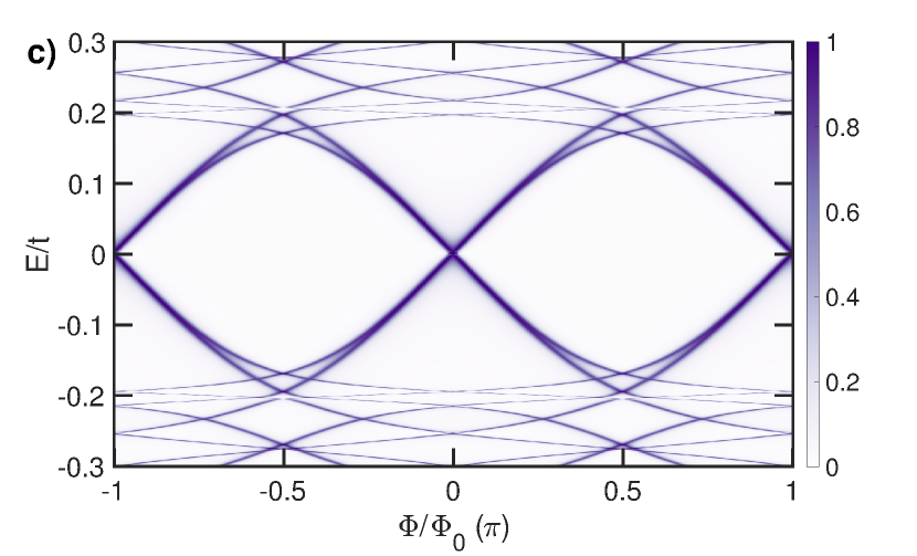
We now consider the transmission probability for an AB ring in the topologically non-trivial regime with an applied magnetic field (, ) shown in Fig. 7c. This is characterised by the presence of a zero energy state at . The MZMs exhibit a linear energy dependence at magnetic flux about where . Just as in Fig. 7b, the ground state of the system is protected against destructive interference at . However now this behaviour extends to the quasi-particle states at both higher and lower energies (). Although the splitting of the zero energy state shows the degeneracy of the ground state is broken by an applied magnetic field, these states are still protected against destructive interference, which is something that is absent in the topologically trivial regime.
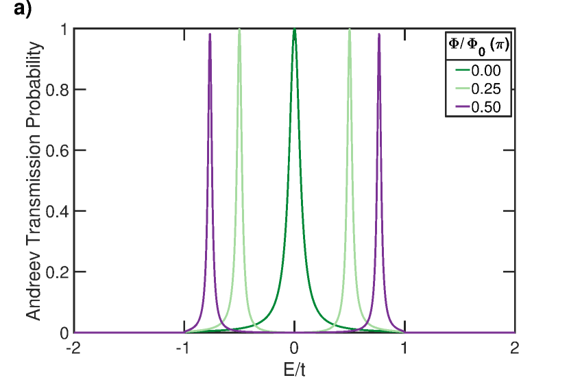
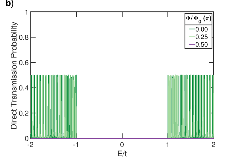
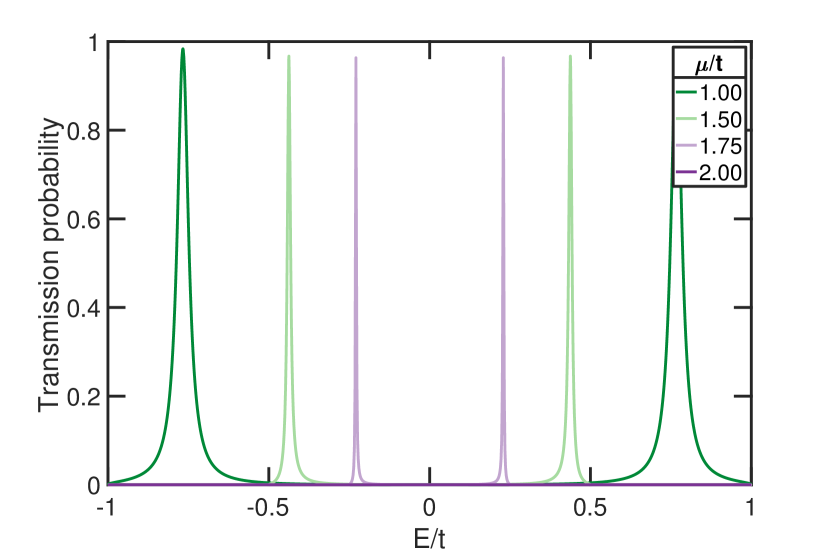
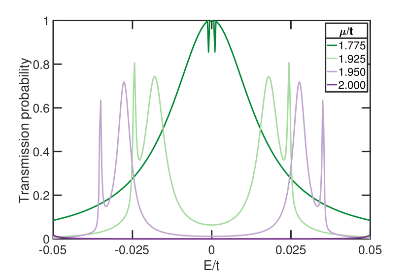
Fig. 8 gives the Andreev and direct transmission for an AB ring when . Crossed Andreev transmission is absent from this figure because it is found to be zero for these parameters. At a magnetic flux we see a zero energy peak for Andreev transmission (Fig. 8a), as well as contributions to the direction transmission from quasi-particle states (Fig. 8b). As the magnetic flux through the ring is varied such that the condition for completely destructive interference is met () we see the suppression of all direct transmission, which is consistent with the behaviour typically observed in AB interference. In contrast to this the Andreev transmission is found to persist at . As with Fig. 7 we see a splitting in the zero energy state that depends on the magnetic flux through the ring and increases with between 0 and . This highlights it is the Andreev transmission that is protected against destructive interference in the AB ring. The extent to which Andreev transmission is protected against destructive interference is shown in Fig. 9, where the transmission probability is plotted as a function of energy for several different values of the on-site potential and a magnetic flux . As the value of the on-site potential is increased and the system moves toward the topologically trivial regime, the width of the sub-gap states becomes vanishingly small.
The absence of destructive interference for an AB ring in the non-trivial regime, as shown in Figs. 7c and 9, is of particular interest. Previous studies have concluded that electrons move through MZMs preserving phase coherence Fu (2010). This would suggest that transport should be suppressed at half integer multiples of magnetic flux quanta (e.g. ), as is typically true for the AB effect. Instead we see a splitting in energy of the topologically non-trivial state, and a shift in the energy of this state away from zero, in response to changing the magnetic flux threading the loop. This raises questions as to whether the topological protection of the MZMs is still preserved in such a situation. It also suggested the response of such a circuit to a magnetic field can be used as a probe of topologically trivial Andreev bound states.
V Effects of disorder
Experimentally realisable systems will contain noise which may perturb the system, one way this can occur is through disorder within the system itself. To study the effect of disorder on our AB rings, we introduce to each site a quasi-random on-site energy which is obtained from a uniform distributionGergs et al. (2016) centred about zero such that . The magnitude of the disorder is controlled via a disorder amplitude such that the on-site term for Eq. 1 becomes .
Electron transport in nanoscale devices is often limited by random offset charges stemming from surfaces and interfaces within the devicePourkabirian et al. (2014); Zorin et al. (1996); Zimmerman et al. (2008); Cedergren et al. (2017); Müller et al. (2019); Gustafsson et al. (2013). This background charge disorder can either be static (approximately constant once the device is cooled to base temperature) or dynamic during the measurement period, resulting in an ensemble averaged signal over multiple disorder realisations.
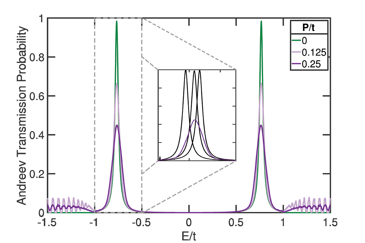
For an AB ring without an applied magnetic field transmission is unchanged by the inclusion of weak disorder. The MZM in such a system is robust against both weak dynamic and static disorder, as seen in literature for 1D wires containing MZMsLieu et al. (2018). However the same is not true for an AB ring in the presence of a magnetic field. Fig. 10 shows the effect of introducing a dynamic disorder scheme into the AB ring with magnetic field applied. The disorder has been introduced in the topologically non-trivial regime where in the form of a random on-site variation. We see that increasing the strength of the disorder broadens the transmission peak and reduces the peak height of the system with dynamic disorder. This reduction in averaged peak height is caused by a disorder induced shifting of the energy values required to achieve peak transmission. This effect is illustrated in the inset, which shows the average transmission for a disorder strength of , with several of the static disorder realisations which have been averaged to get the dynamic disorder result. Note that the peak height for static disorder is unchanged by the strength of the disorder.
The movement of the peaks in the inset of Fig. 10 under disorder may be due to the fluctuations in the on-site potential which causes regions of the ring to transition either deeper into or out of the topologically non-trivial regime. For a system being pushed deeper into the topologically non-trivial regime, the superconducting gap would become larger as in Fig. 4. For a system with magnetic field applied, we see in Fig. 9 that decreasing the on-site potential causes the peaks to move to higher energies. However, that there still exists conductance channels with an applied magnetic field of and in the presence of disorder suggests that these channels are robust against weak disorder.
As the type of disorder affects the resultant transmission peaks, one would expect experimental signatures of the type seen in Fig. 7c to change depending on the type of disorder introduced. Static disorder would cause the separation between the transmission peaks to fluctuate, with the fluctuations increasing in magnitude with disorder strength. However for a system with dynamic disorder, one would expect the separation between the transmission peaks to remain relatively constant, but rather the peak amplitude would be decreased. In both cases, for weak disorder the conduction channels persist in the presence of partially destructive AB interference.
VI Conclusion
We used the NEGF formalism to study the transport properties of an AB ring comprised of two Kitaev chains coupled at either end by a normal link. We observed the effect of electron (hole) interference on the zero-bias transmission of this AB ring, which is present when the magnetic flux through the ring is nonzero. We have shown how the MZMs in this AB ring change with on-site potential , the -wave pairing amplitude , and the magnetic flux through the ring . Each of these parameters has been shown to have a unique effect on the MZMs. Having control of the physical parameters , , and in an experiment therefore allows the MZMs to be probed in a controllable way.
Furthermore, we have observed the transmission probability of electrons and holes through an AB ring with MZMs to be persistent even when the condition for completely destructive interference are met. The power of the NEGF formalism as a tool for investigating this phenomenon is highlighted where the transmission probabilities are divided into three separate contributions: Andreev and crossed Andreev reflection and direct transmission. We have thereby demonstrated that transmission through MZMs in an AB ring is mediated by Andreev reflection at the normal/superconductor interface. The dependence of the AB interference on the parameters of the nanowires is therefore a useful probe of Majorana fermions in condensed matter systems.
The mechanism which provides the above gap states protection from the AB remains unclear. We believe this issue requires further investigation using different tools to those used here and therefore we leave it for further work.
Acknowledgements.
The authors acknowledge useful discussions with S. Rachel, as well as MATLAB code provided by Jesse Vaitkus and Martin Cyster. This work was supported by the Australian Research Council through grants CE170100039 (FLEET) and CE170100009 (EQUS). CM is supported by the Swiss National Science Foundation through NCCR Quantum Science and Technology (QSIT). BM would like to acknowledge funding from the Ministry of Human Resource Development (MHRD), Government of India, Grant no. STARS/APR2019/NS/226/FS under the STARS scheme and the Visvesvaraya Scheme of the Ministry of Electronics and Information Technology (MeiTy), Government of India. This research was undertaken with the assistance of resources from the National Computational Infrastructure, which is supported by the Australian Government.Appendix A Particle-hole symmetry
The Kitaev Hamiltonian when expressed in the BdG form exhibits particle-hole symmetry (PHS). PHS represents a symmetry in the behaviour of electrons and holes and leads to a symmetry in the eigenspectrum around zero energy. As we are investigating a superconducting system, the Hamiltonian contains a coupling term between particles and holes, which is best described in the BdG formalism. Employing the Nambu basis, we group creation and annihilation operators together as
| (13) | ||||
| (14) |
This notation then allows us to write the BdG Hamiltonian as
| (15) |
with the BdG Hamiltonian coefficient matrix for the Kitaev chain:
| (16) |
Here PHS manifests directly in the symmetry between the particle and hole sectors of the Hamiltonian.
Appendix B Derivation of the components of current in a system with particle-hole symmetry
The conventional equation for calculating the transmission of electrons through a device is given in Eq. (4). When applied to a system in conjunction with the BdG form of the Hamiltonian we must also take into consideration the transmission probability for holes. This allows for the study of more transport modes than just the conventional transport of electrons through a device Sriram et al. (2019); Wei et al. (2001); Sun et al. (1999). Andreev and crossed Andreev transmission allow for the reflection of an electron from an interface as a hole both locally and non-locally respectively Law et al. (2009); Wang et al. (2016); Nilsson et al. (2008). In order to probe the role these processes play in this work, Eqs. (8)-(10) were applied. Although here we discuss how Eqs. (8)-(10) can be derived from the Landauer current equations, it is important to note that they are themselves particle transmission functions and not current equations. The distinction being that the transmission functions are independent of the Fermi distribution function (and therefore temperature and lead Fermi levels). These equations are derived from the Landauer current equation:
| (17) |
where is the broadening matrix for lead . We also have
| (18) |
and the spectral function is defined as
| (19) |
Applying these definitions to the Landauer current equation, we arrive at
| (20) |
As we are working in the BdG formalism which utilizes the Nambu (particle-hole) basis, we must take both particle and hole transmission into account. With the application of normal leads there is no coupling between particles and holes and as such the in-scattering matrix () becomes block diagonal (one block for electron scattering and one for hole scattering). We are therefore able to write the in-scattering matrix for lead as
| (21) |
where the superscript e(h) denotes the electron (hole) component in the Nambu basis and is the Fermi distribution for the -lead with Fermi energy at temperature . Combining Eq. (B) and Eq. (21) we arrive at
| (22) |
which after some algebraic manipulation returns
| (23) |
As we only want to study the transmission, rather than the current we can neglect the constant factor as well as the Fermi windowing function, after which we arrive at the transmission equations given in Eqs. (8)-(10).
References
- Majorana and Maiani (2006) Ettore Majorana and Luciano Maiani, “A symmetric theory of electrons and positrons,” in Ettore Majorana Scientific Papers (Springer Berlin Heidelberg, Berlin, Heidelberg, 2006) pp. 201–233.
- Kitaev (2001) A Yu Kitaev, “Unpaired Majorana fermions in quantum wires,” Physics-Uspekhi 44, 131–136 (2001).
- Alicea et al. (2011) Jason Alicea, Yuval Oreg, Gil Refael, Felix Von Oppen, and Matthew P.A. Fisher, “Non-Abelian statistics and topological quantum information processing in 1D wire networks,” Nature Physics 7, 412–417 (2011), arXiv:1006.4395 .
- Lian et al. (2018) Biao Lian, Xiao Qi Sun, Abolhassan Vaezi, Xiao Liang Qib, and Shou Cheng Zhang, “Topological quantum computation based on chiral Majorana fermions,” Proceedings of the National Academy of Sciences of the United States of America 115, 10938–10942 (2018).
- Ivanov (2001) D.A. Ivanov, “Non-Abelian statistics of half-quantum vortices in p-wave superconductors,” Physical Review Letters 86, 268–271 (2001).
- Volovik (1999) G. E. Volovik, “Fermion zero modes on vortices in chiral superconductors,” JETP Letters 70, 609–614 (1999).
- Read and Green (2000) N. Read and Dmitry Green, “Paired states of fermions in two dimensions with breaking of parity and time-reversal symmetries and the fractional quantum Hall effect,” Physical Review B 61, 10267–10297 (2000).
- van Heck et al. (2012) B van Heck, A R Akhmerov, F Hassler, M. Burrello, and C W J Beenakker, “Coulomb-assisted braiding of Majorana fermions in a Josephson junction array,” New Journal of Physics 14, 035019 (2012).
- Kauffman (2016) Louis H. Kauffman, “Knot logic and topological quantum computing with Majorana fermions,” in Logic and Algebraic Structures in Quantum Computing, edited by Jennifer Chubb, Ali Eskandarian, and Valentina Harizanov (Cambridge University Press, Cambridge, 2016) pp. 223–336, arXiv:1301.6214 .
- Kitaev (2003) A.Yu. Kitaev, “Fault-tolerant quantum computation by anyons,” Annals of Physics 303, 2–30 (2003).
- Mourik et al. (2012) V. Mourik, K. Zuo, S. M. Frolov, S. R. Plissard, E. P. A. M. Bakkers, and L. P. Kouwenhoven, “Signatures of Majorana Fermions in Hybrid Superconductor-Semiconductor Nanowire Devices,” Science 336, 1003–1007 (2012).
- Zhang et al. (2018a) Hao Zhang, Chun-Xiao Liu, Sasa Gazibegovic, Di Xu, John A. Logan, Guanzhong Wang, Nick van Loo, Jouri D. S. Bommer, Michiel W. A. de Moor, Diana Car, Roy L. M. Op het Veld, Petrus J. van Veldhoven, Sebastian Koelling, Marcel A. Verheijen, Mihir Pendharkar, Daniel J. Pennachio, Borzoyeh Shojaei, Joon Sue Lee, Chris J. Palmstrøm, Erik P. A. M. Bakkers, S. Das Sarma, and Leo P. Kouwenhoven, “Quantized Majorana conductance,” Nature 556, 74–79 (2018a).
- Law et al. (2009) K. T. Law, Patrick A. Lee, and T. K. Ng, “Majorana Fermion Induced Resonant Andreev Reflection,” Physical Review Letters 103, 237001 (2009).
- Das et al. (2012) Anindya Das, Yuval Ronen, Yonatan Most, Yuval Oreg, Moty Heiblum, and Hadas Shtrikman, “Zero-bias peaks and splitting in an Al–InAs nanowire topological superconductor as a signature of Majorana fermions,” Nature Physics 8, 887–895 (2012).
- Deng et al. (2012) M. T. Deng, C. L. Yu, G. Y. Huang, M. Larsson, P. Caroff, and H. Q. Xu, “Anomalous zero-bias conductance peak in a Nb-InSb nanowire-Nb hybrid device,” Nano Letters 12, 6414–6419 (2012).
- Rokhinson et al. (2012) Leonid P. Rokhinson, Xinyu Liu, and Jacek K. Furdyna, “The fractional a.c. Josephson effect in a semiconductor-superconductor nanowire as a signature of Majorana particles,” Nature Physics 8, 795–799 (2012).
- Deng et al. (2016) M T Deng, S Vaitiekėnas, E B Hansen, J Danon, M Leijnse, K Flensberg, J Nygård, P Krogstrup, and C M Marcus, “Majorana bound state in a coupled quantum-dot hybrid-nanowire system,” Science 354, 1557–1562 (2016).
- Liu et al. (2018) Chun-Xiao Liu, Jay D. Sau, and S. Das Sarma, “Distinguishing topological Majorana bound states from trivial Andreev bound states: Proposed tests through differential tunneling conductance spectroscopy,” Physical Review B 97, 214502 (2018).
- Liu et al. (2017) Chun-Xiao Liu, Jay D. Sau, Tudor D. Stanescu, and S. Das Sarma, “Andreev bound states versus Majorana bound states in quantum dot-nanowire-superconductor hybrid structures: Trivial versus topological zero-bias conductance peaks,” Physical Review B 96, 075161 (2017).
- Moore et al. (2018a) Christopher Moore, Tudor D. Stanescu, and Sumanta Tewari, “Two-terminal charge tunneling: Disentangling Majorana zero modes from partially separated Andreev bound states in semiconductor-superconductor heterostructures,” Physical Review B 97, 165302 (2018a).
- Deng et al. (2018) M.-T. Deng, S. Vaitiekenas, E. Prada, P. San-Jose, J. Nygård, P. Krogstrup, R. Aguado, and C. M. Marcus, “Nonlocality of Majorana modes in hybrid nanowires,” Physical Review B 98, 085125 (2018).
- Chiu and Das Sarma (2019) Ching-Kai Chiu and S. Das Sarma, “Fractional Josephson effect with and without Majorana zero modes,” Physical Review B 99, 035312 (2019).
- Moore et al. (2018b) Christopher Moore, Chuanchang Zeng, Tudor D. Stanescu, and Sumanta Tewari, “Quantized zero-bias conductance plateau in semiconductor-superconductor heterostructures without topological Majorana zero modes,” Physical Review B 98, 155314 (2018b).
- Chen et al. (2014) Lei Chen, W. LiMing, Jia-Hui Huang, Chengping Yin, and Zheng-Yuan Xue, “Majorana zero modes on a one-dimensional chain for quantum computation,” Physical Review A 90, 012323 (2014).
- Alicea (2012) Jason Alicea, “New directions in the pursuit of Majorana fermions in solid state systems,” Reports on Progress in Physics 75, 076501 (2012).
- Lee et al. (2014) Minchul Lee, Heunghwan Khim, and Mahn-Soo Choi, “Anomalous crossed Andreev reflection in a mesoscopic superconducting ring hosting Majorana fermions,” Physical Review B 89, 035309 (2014).
- Doornenbal et al. (2015) R. J. Doornenbal, G. Skantzaris, and H. T. C. Stoof, “Conductance of a finite Kitaev chain,” Physical Review B 91, 045419 (2015).
- Weithofer et al. (2014) Luzie Weithofer, Patrik Recher, and Thomas L. Schmidt, “Electron transport in multiterminal networks of Majorana bound states,” Physical Review B 90, 205416 (2014).
- Danon et al. (2020) Jeroen Danon, Anna Birk Hellenes, Esben Bork Hansen, Lucas Casparis, Andrew P Higginbotham, and Karsten Flensberg, “Nonlocal Conductance Spectroscopy of Andreev Bound States: Symmetry Relations and BCS Charges,” Physical Review Letters 124, 036801 (2020).
- van Heck et al. (2011) B. van Heck, F. Hassler, A. R. Akhmerov, and C. W. J. Beenakker, “Coulomb stability of the 4-periodic Josephson effect of Majorana fermions,” Physical Review B 84, 180502(R) (2011), arXiv:1108.1095 .
- Zeng et al. (2017) Qi-Bo Zeng, Shu Chen, L. You, and Rong Lü, “Transport through a quantum dot coupled to two Majorana bound states,” Frontiers of Physics 12, 127302 (2017).
- Akhmerov et al. (2011) A.R. Akhmerov, J.P. Dahlhaus, F. Hassler, M. Wimmer, and C.W.J. Beenakker, “Quantized Conductance at the Majorana Phase Transition in a Disordered Superconducting Wire,” Physical Review Letters 106, 057001 (2011).
- Whiticar et al. (2020) A M Whiticar, A Fornieri, E. C. T. O’Farrell, A. C. C. Drachmann, T Wang, C Thomas, S Gronin, R Kallaher, G C Gardner, M J Manfra, C M Marcus, and F Nichele, “Coherent transport through a Majorana island in an Aharonov–Bohm interferometer,” Nature Communications 11, 3212 (2020).
- Tripathi et al. (2016) Krashna Mohan Tripathi, Sourin Das, and Sumathi Rao, “Fingerprints of Majorana Bound States in Aharonov-Bohm Geometry,” Physical Review Letters 116, 166401 (2016).
- Shang et al. (2014) En-Ming Shang, Yi-Ming Pan, Lu-Bing Shao, and Bai-Gen Wang, “Detection of Majorana fermions in an Aharonov—Bohm interferometer,” Chinese Physics B 23, 057201 (2014).
- Benjamin and Pachos (2010) Colin Benjamin and Jiannis K Pachos, “Detecting Majorana bound states,” Physical Review B 81, 085101 (2010).
- Hansen et al. (2016) Esben Bork Hansen, Jeroen Danon, and Karsten Flensberg, “Phase-tunable Majorana bound states in a topological N-SNS junction,” Physical Review B 93, 94501 (2016).
- Jiang and Zheng (2015) Cui Jiang and Yi-Song Zheng, “Fano effect in the Andreev reflection of the Aharonov-Bohm-Fano ring with Majorana bound states,” Solid State Communications 212, 14–18 (2015).
- Haug et al. (2019a) Tobias Haug, Rainer Dumke, Leong-Chuan Kwek, and Luigi Amico, “Andreev-reflection and Aharonov–Bohm dynamics in atomtronic circuits,” Quantum Science and Technology 4, 045001 (2019a).
- Haug et al. (2019b) Tobias Haug, Hermanni Heimonen, Rainer Dumke, Leong-Chuan Kwek, and Luigi Amico, “Aharonov-Bohm effect in mesoscopic Bose-Einstein condensates,” Physical Review A 100, 041601(R) (2019b).
- Haug et al. (2019c) Tobias Haug, Rainer Dumke, Leong-Chuan Kwek, and Luigi Amico, “Topological pumping in Aharonov–Bohm rings,” Communications Physics 2, 127 (2019c).
- Qin et al. (2019) Lupei Qin, Xin-Qi Li, Alexander Shnirman, and Gerd Schön, “Transport signatures of a Majorana qubit and read-out-induced dephasing,” New Journal of Physics 21, 043027 (2019).
- Val’kov et al. (2019) V V Val’kov, M Yu Kagan, and S V Aksenov, “Fano effect in Aharonov-Bohm ring with topologically superconducting bridge,” Journal of Physics: Condensed Matter 31, 225301 (2019).
- Aksenov and Kagan (2020) S. V. Aksenov and M. Yu. Kagan, “Collapse of the Fano Resonance Caused by the Nonlocality of the Majorana State,” JETP Letters 111, 286–292 (2020).
- Park et al. (2014) Sunghun Park, Joel E. Moore, and H.-S. Sim, “Absence of the Aharonov-Bohm effect of chiral Majorana fermion edge states,” Physical Review B 89, 161408(R) (2014).
- Fu and Kane (2009) Liang Fu and C. L. Kane, “Probing Neutral Majorana Fermion Edge Modes with Charge Transport,” Physical Review Letters 102, 216403 (2009).
- Zvyagin (2015) A. A. Zvyagin, “Majorana bound states in the finite-length chain,” Low Temperature Physics 41, 625–629 (2015).
- Leumer et al. (2020) Nico Leumer, Magdalena Marganska, Bhaskaran Muralidharan, and Milena Grifoni, “Exact eigenvectors and eigenvalues of the finite Kitaev chain and its topological properties,” Journal of Physics: Condensed Matter 32, 445502 (2020).
- Zhang et al. (2018b) Ya Jing Zhang, Shuai Zhang, Guang Yu Yi, Cui Jiang, and Wei Jiang Gong, “Interference effects in the Aharonov-Bohm geometries with Majorana bound states,” Superlattices and Microstructures 113, 25–33 (2018b).
- Datta (2005) Supriyo Datta, Quantum Transport: Atom to Transistor (Cambridge University Press, Cambridge, 2005).
- Lundstrom (2000) Mark Lundstrom, Fundamentals of Carrier Transport (Cambridge University Press, 2000).
- Peierls (1933) R. Peierls, “Zur Theorie des Diamagnetismus von Leitungselektronen,” Zeitschrift fur Physik 80, 763–791 (1933).
- Maśka and Mierzejewski (2001) Maciej M. Maśka and Marcin Mierzejewski, “Upper critical field for anisotropic superconductivity: A tight-binding approach,” Physical Review B 64, 064501 (2001).
- Hofstadter (1976) Douglas R. Hofstadter, “Energy levels and wave functions of Bloch electrons in rational and irrational magnetic fields,” Physical Review B 14, 2239–2249 (1976).
- Bosland et al. (1992) P. Bosland, F. Guemas, M. Juillard, M. Couach, and A.F. Khoder, “NbTiN superconducting thin films prepared by magnetron sputtering.” (Editions Frontieres, 1992) pp. 1316–1318.
- Di Leo et al. (1990) R. Di Leo, A. Nigro, G. Nobile, and R. Vaglio, “Niboium-titanium nitride thin films for superconducting rf accelerator cavities,” Journal of Low Temperature Physics 78, 41–50 (1990).
- Fu (2010) Liang Fu, “Electron Teleportation via Majorana Bound States in a Mesoscopic Superconductor,” Physical Review Letters 104, 056402 (2010).
- Gergs et al. (2016) Niklas M Gergs, Lars Fritz, and Dirk Schuricht, “Topological order in the Kitaev/Majorana chain in the presence of disorder and interactions,” Physical Review B 93, 075129 (2016).
- Pourkabirian et al. (2014) A. Pourkabirian, M. V. Gustafsson, G. Johansson, J. Clarke, and P. Delsing, “Nonequilibrium Probing of Two-Level Charge Fluctuators Using the Step Response of a Single-Electron Transistor,” Physical Review Letters 113, 256801 (2014).
- Zorin et al. (1996) A. B. Zorin, F.-J. Ahlers, J. Niemeyer, T. Weimann, H. Wolf, V. A. Krupenin, and S. V. Lotkhov, “Background charge noise in metallic single-electron tunneling devices,” Physical Review B 53, 13682–13687 (1996).
- Zimmerman et al. (2008) Neil M. Zimmerman, William H. Huber, Brian Simonds, Emmanouel Hourdakis, Akira Fujiwara, Yukinori Ono, Yasuo Takahashi, Hiroshi Inokawa, Miha Furlan, and Mark W. Keller, “Why the long-term charge offset drift in Si single-electron tunneling transistors is much smaller (better) than in metal-based ones: Two-level fluctuator stability,” Journal of Applied Physics 104, 033710 (2008).
- Cedergren et al. (2017) Karin Cedergren, Roger Ackroyd, Sergey Kafanov, Nicolas Vogt, Alexander Shnirman, and Timothy Duty, “Insulating Josephson Junction Chains as Pinned Luttinger Liquids,” Physical Review Letters 119, 167701 (2017).
- Müller et al. (2019) Clemens Müller, Jared H Cole, and Jürgen Lisenfeld, “Towards understanding two-level-systems in amorphous solids: insights from quantum circuits,” Reports on Progress in Physics 82, 124501 (2019).
- Gustafsson et al. (2013) Martin V. Gustafsson, Arsalan Pourkabirian, Göran Johansson, John Clarke, and Per Delsing, “Thermal properties of charge noise sources,” Physical Review B 88, 245410 (2013).
- Lieu et al. (2018) Simon Lieu, Derek K. K. Lee, and Johannes Knolle, “Disorder protected and induced local zero-modes in longer-range Kitaev chains,” Physical Review B 98, 134507 (2018).
- Sriram et al. (2019) Praveen Sriram, Sandesh S Kalantre, Kaveh Gharavi, Jonathan Baugh, and Bhaskaran Muralidharan, “Supercurrent interference in semiconductor nanowire Josephson junctions,” Physical Review B 100, 155431 (2019).
- Wei et al. (2001) Yadong Wei, Jian Wang, Hong Guo, Hatem Mehrez, and Christopher Roland, “Resonant Andreev reflections in superconductor–carbon-nanotube devices,” Physical Review B 63, 195412 (2001).
- Sun et al. (1999) Qing-feng Sun, Jian Wang, and Tsung-han Lin, “Resonant Andreev reflection in a normal-metal–quantum-dot–superconductor system,” Physical Review B 59, 3831–3840 (1999).
- Wang et al. (2016) Su-Xin Wang, Yu-Xian Li, and Jian-Jun Liu, “Resonant Andreev reflection in a normal-metal/quantum-dot/superconductor system with coupled Majorana bound states,” Chinese Physics B 25, 037304 (2016).
- Nilsson et al. (2008) Johan Nilsson, A. R. Akhmerov, and C. W. J. Beenakker, “Splitting of a Cooper Pair by a Pair of Majorana Bound States,” Physical Review Letters 101, 120403 (2008).