Thermoelectric figure of merit enhancement in dissipative superlattice structures
Abstract
Utilizing the non-coherent quantum transport formalism, we investigate thermoelectric performance across dissipative superlattice configurations in the linear regime of operation. Using the dissipative non-equilibrium Green’s function formalism coupled self-consistently with the Poisson’s equation, we report an enhanced figure of merit in the multi-barrier device designs. The proposed enhancement, we show, is a result of a drastic reduction in the electronic thermal conductance triggered via non-coherent transport. We show that a maximum value of 18 can be achieved via the inclusion of non-coherent elastic scattering processes. There is also a reasonable enhancement in the Seebeck coefficient, with a maximum of , which we attribute to an enhancement in electronic filtering arising from the non-coherent transport. Distinctly the thermal conduction is drastically reduced as the length of the superlattice scales up, although the power factor shows an overall degradation. While the presence of interfaces is known to kill phonon thermal conduction, our analysis shows that non-coherent processes in superlattice structures can effectively kill electronic thermal conduction also. We believe that the analysis presented here could set the stage to understand better the interplay between non-coherent scattering and coherent quantum processes in the electronic engineering of heterostructure thermoelectric devices.
I Introduction
Thermoelectric (TE) materials, structures or devices are typically assessed via the dimensionless figure of merit that is directly related to its energy conversion efficiency. Here is the Seebeck coefficient (thermopower), the electrical conductivity, the electronic (phonon) contribution to the thermal conductivity and the operating temperature Ioffe (1956); Rowe (2005); Goldsmid (2010). In the past two and a half decades, a great deal of research has been carried out in pursuit of an increase in ‘’, from the conventional bulk to nanostructured thermoelectric materials Majumdar (2004); Snyder and Toberer (2008); Minnich et al. (2009).
Using nanostructuring concepts, a higher value of was shown to be achieved by either increasing the numerator or decreasing the denominator part of the figure of merit definition. The numerator is called the power factor (PF ), which mainly constitutes electronic transport in the ballistic or diffusive limit Fisher (2014). The denominator part is a combination of thermal conduction due to electrons as well as phonons, so there is a trade-off between the PF and the thermal conductivity Minnich (2011); Muralidharan and Grifoni (2012); De and Muralidharan (2016a, b, 2019). An important direction enroute, apart from engineering the reduction of phonon thermal conductivity via enhanced scattering at nano-interfaces Minnich et al. (2009); Singha et al. (2015); Singha and Muralidharan (2017), has been in the direction of low-dimensional nanostructuring to enhance the electronic figure of merit via a distortion in the electronic density of states Hicks and
Dresselhaus (1993a, b); Hicks et al. (1996); Heremans et al. (2013); Broido and Reinecke (1995); Balandin and Lazarenkova (2003); Kim et al. (2009); Kim and Lundstrom (2011); Mao et al. (2016).
As an ultimate example of electronic engineering, it was mathematically proposed that a Dirac-delta transport function can lead to an infinite electronic figure of merit and a conversion efficiency tending to the Carnot limit Mahan and Sofo (1996). But, the electrical power drawn at this efficiency would be zero in accordance with reversible thermodynamics, whereas, the ideal thermoelectric effect is an irreversible process accompanied by a finite power generation Nakpathomkun et al. (2010); Muralidharan and Grifoni (2012); Sothmann et al. (2013) . In this context, it was clearly postulated Whitney (2014, 2015) that under the situation of drawing the maximum power at a given efficiency, the ideal electronic transmission would assume a ’box car’ or a band pass filtering shape. In this context, a superlattice structure fits very well where mini-bands can be engineered to assume the box car transmission function.
While the idea to use superlattice (SL) structures in thermoelectrics was proposed to enable the suppression of the cross-plane thermal conduction without affecting the condition that enhances the electronic power factor Yang et al. (2018); Xiao and Zhao (2015), the idea of using mini-bands in SL structures was also recently proposed in various theoretical effortsKarbaschi et al. (2016); Mukherjee et al. (2018); Priyadarshi et al. (2018); Mukherjee and Muralidharan (2019). It is noted that the phonon mean free path is greater than the size of nanostructures, while the electron mean free path is smaller Fisher (2014); Wang and Wang (2014), giving plenty of room for electronic engineering Datta (2012). While the previous works Karbaschi et al. (2016); Mukherjee et al. (2018); Priyadarshi et al. (2018); Mukherjee and Muralidharan (2019) focused on the analysis in the ballistic regime, we advance the framework to examine various superlattice structures depicted in Fig. 1 in the dissipative regime Singha and Muralidharan (2017, 2018), in the presence of electron phonon interactions treated in the form of Büttiker probes Datta (2005, 2012). Most importantly, the systematic introduction of scattering processes puts us into an interesting perspective where the effects of coherent processes like tunneling and mini-band formation compete with the relaxation processes induced via scattering Singha and Muralidharan (2017, 2018).
In the realm of proposed SL structures, electronic analogs of the optical concept of anti-reflective layers Pacher et al. (2001); Morozov et al. (2002); Priyadarshi et al. (2018); Mukherjee et al. (2018) have also been proposed recently and analyzed in detail as potential candidates for enhanced TE performance. In this paper, we consider normal and anti-reflective superlattice structures Pacher et al. (2001); Morozov et al. (2002); Priyadarshi et al. (2018); Mukherjee et al. (2018) that are optimally configured in order to analyze the TE properties. We use the miniband transmission feature of the superlattice to set the device Fermi energy level for positive TE transport Priyadarshi et al. (2018, 2019); Priyadarshi and Muralidharan (2020). Using the non-equilibrium Green’s function(NEGF) formalism coupled self-consistently with the Poisson’s equation, we report an enhanced figure of merit in the multi-barrier device designs. The proposed enhancement is a result of a drastic reduction in the electronic thermal conductance triggered via non-coherent transport. We show that a maximum value of 18 can been achieved via the inclusion of non-coherent elastic scattering processes in the electron transport. There is also a reasonable enhancement in the Seebeck coefficient, with a maximum of , which we attribute to an enhancement in electronic filtering arising from the non-coherent transport. Distinctly the thermal conduction is drastically reduced as the length of the superlattice scales up, although the power factor shows an overall degradation. While the presence of interfaces is known to kill phonon thermal conduction, our analysis shows that non-coherent processes in superlattice structures can effectively kill electronic thermal conduction also. We believe that the analysis presented here could set the stage to understand better the interplay between non-coherent scattering and coherent quantum processes in the electronic engineering of heterostructure thermoelectric devices.
II Superlattice Structure and Computational Formalism
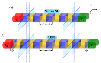
Figure 1 shows the schematic of a heterostructure thermoelectric device set up, where the two contacts are maintained at temperatures (hot) and (cold), respectively. For building the heterostructure, we choose the GaAs/AlGaAs material system because the lattice constant and the conduction band effective masses are almost the same at small proportion of Al in GaAs. The central channel region of the superlattice configuration in Fig. 1(a), depicts an alternate well-barrier structure in the transport direction, labeled as Normal SL. The overall device size depends on the number of barriers used, where one unit consist of a barrier of thickness and a well region of width , successively. Similarly, Fig. 1(b), labeled ARSL (anti-reflective SL), depicts the normal superlattice (NSL) configuration in addition with the two extra half barriers () or the anti-reflective barriers are attached at both the ends after a well region Pacher et al. (2001); Morozov et al. (2002); Priyadarshi et al. (2018); Mukherjee et al. (2018).
We perform a one dimensional carrier transport simulations along the direction in the described SL configurations. To calculate the thermoelectric parameters, we operate our devices in the linear response regime. In this scenario, the thermoelectric dimensionless figure of merit for electronic transport only is calculated as
| (1) |
where being the Seebeck coefficient, , and are the electrical and thermal conductances across the device. Here, is the average temperature of the hot () and cold () contacts. To calculate the quantities in (1), we invoke the coupled charge and heat current equations in the linear regime of operation Datta (2012); Kim and Lundstrom (2011), given as
| (2) |
and
| (3) |
In general, the quantities , , , are related to the Onsager coefficients Datta (2012), under an applied bias and a temperature difference .
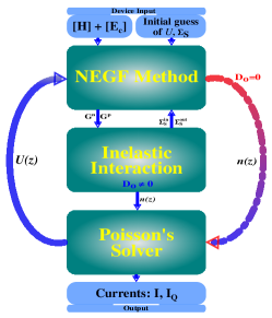
To calculate these transport coefficients, we employ the dissipative non-equilibrium Green’s function (NEGF) formalism self-consistent with the Poisson charging effect Datta (2005), elaborated in Fig. 2. The simulation starts with the formation of device Hamiltonian obtained herewith the nearest neighbor tight-binding model. The variation in SL configurations is captured in the form of device potential profile . The general dissipative model of quantum transport starts with the energy-resolved retarded matrix representation of the retarded Green’s function , given by
| (4) |
where is the energy of the electronic wave function, is the identity matrix, , and are the self-energy matrices of hot and cold contacts, respectively. For the electron-phonon interaction, the scattering matrix is calculated as
| (5) |
where and are the in-scattering and the out-scattering matrices which model the rate of scattering of the electrons due to electron-phonon interactions Datta (2005). These scattering matrices are related to the electron (]) and the hole correlation () functions, given by
| (6) |
with
| (7) |
where is the scattering strength, and is the phonon frequency, which in the elastic case dealt with in this paper is taken to be zero. We focus on momentum and phase relaxation mechanisms Datta (2005, 2012) that are phenomenologically modeled via the the scattering strength . Commonly, elastic interactions include phase breaking processes like momentum relaxation caused by acoustic phonons, electron-electron scattering and other possible near elastic processes. The above formalism of varying is also commonly used as a Büttiker probe style calculation to demonstrate the smooth transition from coherent transport to diffusive transport Datta (2005, 2012), and serves the critical purpose of “systematically” adding such phase breaking processes over the coherent transport layer. The electron and the hole correlation functions are again related to the electrons in-scattering and out-scattering matrices through the equations:
| (8) |
The complete in-scattering and out-scattering functions are calculated as:
| (9) |
and
| (10) |
where is the Fermi-Dirac distribution function of the hot (cold) contact and represents the broadening matrix of the hot (cold) contact. The Equations (4) -(7) are calculated self-consistently with some initial guess of . The bias potential and the charging effect are encapsulated in the matrix . The electronic charging effect is calculated using a self-consistent Poisson’s equation in the transport direction , given by
| (11) |
where is the electronic charge, is the free space (relative) permittivity. The electron density along the transport direction is calculated as,
| (12) |
where is the unit length and is the diagonal element of energy resolved electron correlation function . The self-consistent solution of (4)-(12) is used to calculate the currents across two discrete device points and as
| (13) |
where, represents the element of the matrix and
| (14) |
where is the electronic heat current, originating from the hot contact . We can then evaluate the Seebeck coefficient as:
| (15) |
where is the electrical conductance obtained from (2) by making at a small bias voltage that ensures the linear response operation. Similarly, from (2), is obtained by setting at a finite . Likewise from (3), the quantity is calculated by keeping and when are obtained. Now that we have all the transport coefficients the electronic thermal conductance is given by
| (16) |
Using the above calculations of the linear response parameters via actual current calculations in the presence of scattering, we now proceed to analyze the thermoelectric performance of various superlattice structures.
III Results and Discussion
In the following section, we present the simulation results of superlattice TE performance parameters in the linear regime of operation. We will compare notes on how the elastic carrier scattering influences the TE parameters obtained from the coherent and non-coherent quantum thermoelectric transport methodology. In Tab. 1, we enlist the parameter set for the calculations performed in this paper.
III.1 Effect of Fermi Energy on TE Parameters
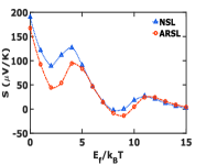
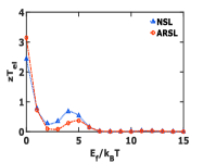
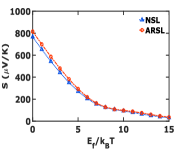
Figure 3 shows the variation of the Seebeck coefficient, and the electronic figure of merit, as a function of channel Fermi level , when the coherent transport simulation set up is active (as described in Fig. 2). For both the SL configurations (NSL & ARSL), the maximum is found at , as shown in Fig. 3, and thereafter it decreases. Likewise, the Seebeck coefficient is maximum at zero , shown in Fig. 3. This fact can be argued on the basis of the physics of thermoelectric transport, where the position of needs to below from the lower edge of transmission spectra Priyadarshi et al. (2019), to achieve positive TE transport. In general, the position of governs the carrier concentration in the channel region, and thus on increasing (manually, in this work), we force the semiconductor to be degenerate. Although the electrical conduction is comparatively very close to the metal in a degenerate semiconductor, the thermopower () decreases on the same note. The Fermi level position is, therefore, an essential parameter in determining the TE performance of the concerned systems.
| SL | Parameters | Value | Unit |
|---|---|---|---|
| 1.) | Kelvin | ||
| 2.) | Kelvin | ||
| 3.) | 0.07 | ||
| 4.) | 0.1 | ||
| 5.) | (step size) | ||
| 6.) | (scattering strength) | ||
| 7.) | Well width | ||
| 8.) | Barrier thickness |
We infer from the plots in Fig. 3, that there is not any practical advantage of using ARSL over NSL due to the inclusion of charging effect, as discussed in our previous work Priyadarshi et al. (2018). The reaches a maximum value of and in the NSL and ARSL device configurations at zero , respectively. Furthermore, at higher , the NSL overtakes the ARSL configuration due to the mismatch of minibands and Fermi window at higher energies Pacher et al. (2001). Thereby, we can say that by using the optimized superlattice structures, one can achieve a higher as compared to the bulk TE counterpart.
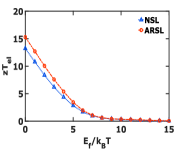
Now, we incorporate the elastic scattering in our calculations due to the phonon interaction and observe the variation in results obtained from coherent transport. In Figs. 4 & 4, the Seebeck coefficient and is plotted respectively as a function of , by enabling the interaction block as described in Fig. 2, for the 5-barrier NSL and ARSL configurations. Unlike the plots in Fig.3, both quantities decrease gradually with the Fermi level, from the maximum value at . Surprisingly, we achieve a maximum of 13 and 15 at (shown in Fig. 4) for the NSL and ARSL, respectively. This indicates that when we include the phonon interaction in electron transport, the TE parameters get improved. Likewise, the Seebeck coefficient enhances to a value of in NSL and around in the case of ARSL.
III.2 Scaling Effect
To explore the effect of device length on the TE parameters, we vary the number of barriers in the central channel region of the device configurations keeping all the simulation parameters the same. In Fig. 5, we plot the figure of merit as a function of the number of barriers for the coherent and non-coherent electron transport.
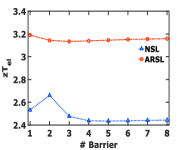
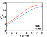
We note from Fig. 5, that the value of increases to 2.7 for 2-barrier NSL configuration and thereafter saturates around 2.4, in the case of coherent transport. In the case of ARSL, remains around 3.2, irrespective of the device length. We note here, that the use of anti-reflective layer in the superlattice enhances the figure of merit by 30%, while ignoring the phonon interaction in electronic transport. The similar calculation approach, now enabling the elastic interaction block (), is taken to plot the variation of as a function of device length. From Fig. 5, we notice that the figure of merit gets improved in both the cases, contrarily when . The parameter gradually increases with the device length, but slightly higher in the ARSL configuration. The maximum numerical value of we obtain here is approximately 17 & 18 in 8-barrier NSL and ARSL configurations, respectively. Beyond this device length, the value gets saturated. This can be understood by the fact that when we increase the number of barriers in the channel region, the mean free path of phonons gets diminished Sofo and Mahan (1994); Broido and Reinecke (1995); Balandin and Lazarenkova (2003) and thus doesn’t affect the flow of electrons through the channel.
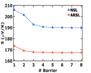
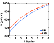
Figure 6 shows the variation of the Seebeck coefficient as a function of number of barriers for the one dimensional transport calculation. From Fig. 6, it is evident that the value of in NSL configuration is better than the ARSL configuration when no interaction is included. But, taking the elastic scattering into account, the Seebeck coefficient enhances in both device structures, shown in Fig. 6. Here, we get an advantage in the case of ARSL configuration and thus reaches up to a value of at 8-barriers. Generically, there is a reduction in the electronic conduction as we increase the barriers in the channel; however, the Seebeck coefficient increases as mathematically observed from the (15). Thus, there is a trade-off between the electrical conductance and the Seebeck coefficient , when the device is forced to operate in the non-linear regime.
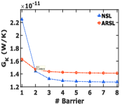
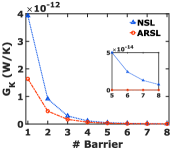
The above analysis, so far, can also be supported by the conduction of heat carried out by the electrons in the device. While lattice phonons also contribute to the thermal conduction, the superlattice interfaces and boundaries affect its flow Chen (2005). Here, we calculate the electronic part of the thermal conduction, as explained in the (16), and demonstrate that such interfaces also affect the electronic heat flow in the presence of elastic scattering. In Fig. 7, the variation of thermal conduction () as a function of number of barriers is shown. On comparing the plots from Figs. 7 & 7, the thermal conduction () is greatly reduced by a factor of 10 when we include the interaction part in the calculations. We also note from Fig. 7 that the value is almost zero, however in the case of ARSL, it approaches as low as (shown in the inset of Fig. 7), for the 8-barrier device length. The optimum layer thickness and stoichiometry proportion of the superlattice structures shrink the mean free path or wavelength of the heat carriers (i.e. phonons in semiconductor) imposes an additional resistance to the thermal transport and thus reduces the thermal conduction.
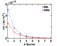
To benchmark a TE material or device structure, the quantity power factor (PF) that defines a practical application of the TE power generator. For a functional power generator, one has to look for the maximum power factor. However, it is challenging to enhance PF without disturbing the other thermoelectric coefficients, as explained via the inconsistency between and . Although it is suggested that in a superlattice where carriers are confined within a thin layer (here in the transport direction ) one can enhance the PF Hicks and
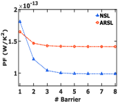
Dresselhaus (1993a, b). We plot the variation of PF as a function of number of barriers in Figs. 8 & 8 for the coherent and non-coherent simulation setups, respectively. In both the SL configurations, the value of PF decreases with the number of barriers. Similarly, when the elastic scattering is taken into account the PF value is reduced by a factor of 10. This could be understood by rationally observing the reduction of electrical conduction in the lengthy device.
The results, particularly those of Fig. 7 and Fig. 8, elucidate the role of elastic scattering in the drastic reduction of electronic thermal conductance, albeit a decrease power factor as a result of a corresponding decrease in electrical conductance. Coupled with the increase in Seebeck coefficient due to electronic filtering effects of the ”box car” transmission function, our results demonstrate the interplay of coherent quantum effects dictated by electronic filtering along with scattering effects as a route toward electronic engineering of thermoelectric structures. While the presence of interfaces is known to kill phonon thermal conduction, our analysis shows that non-coherent processes in superlattice structures can effectively kill electronic thermal conduction also.
IV Conclusion
Using the dissipative non-equilibrium Green’s function formalism coupled self-consistently with the Poisson’s equation, we reported an enhanced figure of merit in the multi-barrier device designs. The proposed enhancement is a result of a drastic reduction in the electronic thermal conductance triggered via non-coherent transport. We show that a maximum value of 18 can been achieved via the inclusion of non-coherent elastic scattering processes in the electron transport. There is also a reasonable enhancement in the Seebeck coefficient, with a maximum of , which we attribute to an enhancement in electronic filtering arising from the non-coherent transport. Distinctly the thermal conduction is drastically reduced as the length of the superlattice scales up, although the power factor shows an overall degradation. We believe that the analysis presented here could set the stage to understand better the interplay between non-coherent scattering and coherent quantum processes in the electronic engineering of heterostructure thermoelectric devices.
Acknowledgements: The Research and Development work undertaken in the project under the Visvesvaraya Ph.D. Scheme of Ministry of Electronics and Information Technology, Government of India, is implemented by Digital India Corporation (formerly Media
Lab Asia). This work was also supported by the Science and
Engineering Research Board (SERB), Government of
India, Grant No. EMR/2017/002853 and Grant No. STR/2019/000030.
References
- Ioffe (1956) A. F. Ioffe, Semiconductor Thermoelements and Thermoelectric Cooling (Infosearch Ltd., 1956).
- Rowe (2005) D. M. Rowe, Introduction to Thermoelectricity (CRC Press, 2005).
- Goldsmid (2010) H. J. Goldsmid, Introduction to Thermoelectricity, Springer Series in Materials Science (Springer, 2010).
- Majumdar (2004) A. Majumdar, Science 303, 777 (2004).
- Snyder and Toberer (2008) G. J. Snyder and E. S. Toberer, Nature Materials 7, 105 (2008).
- Minnich et al. (2009) A. J. Minnich, M. S. Dresselhaus, Z. F. Ren, and G. Chen, Energy Environ. Sci. 2, 466 (2009).
- Fisher (2014) T. S. Fisher, Thermal Energy At The Nanoscale, vol. 3 of Lessons from Nanoscience: A Lecture Notes (World Scientific, 2014).
- Minnich (2011) A. J. Minnich, Ph.D. thesis, Massachusetts Institute of Technology, Cambridge, Massachusetts (2011).
- Muralidharan and Grifoni (2012) B. Muralidharan and M. Grifoni, Physical Review B 85, 1 (2012).
- De and Muralidharan (2016a) B. De and B. Muralidharan, Phys. Rev. B 94, 165416 (2016a).
- De and Muralidharan (2016b) B. De and B. Muralidharan, Scientific Reports 8 (2016b).
- De and Muralidharan (2019) B. De and B. Muralidharan, Journal of Physics: Condensed Matter 32, 035305 (2019).
- Singha et al. (2015) A. Singha, S. D. Mahanti, and B. Muralidharan, AIP Advances 5, 107210 (2015).
- Singha and Muralidharan (2017) A. Singha and B. Muralidharan, Scientific Reports 7, 1 (2017).
- Hicks and Dresselhaus (1993a) L. D. Hicks and M. S. Dresselhaus, Physical Review B 47, 727 (1993a).
- Hicks and Dresselhaus (1993b) L. D. Hicks and M. S. Dresselhaus, Physical Review B 47, 8 (1993b).
- Hicks et al. (1996) L. D. Hicks, T. C. Harman, X. Sun, and M. S. Dresselhaus, Physical Review B 53, R10493 (1996).
- Heremans et al. (2013) J. P. Heremans, M. S. Dresselhaus, L. E. Bell, and D. T. Morelli, Nature Nanotechnology 8, 471 (2013).
- Broido and Reinecke (1995) D. A. Broido and T. L. Reinecke, Physical Review B 51, 13797 (1995).
- Balandin and Lazarenkova (2003) A. A. Balandin and O. L. Lazarenkova, Applied Physics Letters 82, 415 (2003).
- Kim et al. (2009) R. Kim, S. Datta, and M. S. Lundstrom, Journal of Applied Physics 105, 034506 (2009).
- Kim and Lundstrom (2011) R. Kim and M. S. Lundstrom, Journal of Applied Physics 110, 034511 (2011).
- Mao et al. (2016) J. Mao, Z. Liu, and Z. Ren, npj Quantum Materials 1, 16028 (2016).
- Mahan and Sofo (1996) G. D. Mahan and J. O. Sofo, Proceedings of the National Academy of Sciences 93, 7436 (1996).
- Nakpathomkun et al. (2010) N. Nakpathomkun, H. Q. Xu, and H. Linke, Physical Review B 82 (2010).
- Sothmann et al. (2013) B. Sothmann, R. Sánchez, A. N. Jordan, and M. Büttiker, New Journal of Physics 15, 095021 (2013).
- Whitney (2014) R. S. Whitney, Physical Review Letters 112, 1 (2014).
- Whitney (2015) R. S. Whitney, Physical Review B 91, 1 (2015).
- Yang et al. (2018) G. Yang, J. Pan, X. Fu, Z. Hu, Y. Wang, Z. Wu, E. Mu, X.-J. Yan, and M.-H. Lu, Nano Convergence 22 (2018).
- Xiao and Zhao (2015) Y. Xiao and L.-D. Zhao, npj Quantum Materials 3, 1 (2015).
- Karbaschi et al. (2016) H. Karbaschi, J. Lovén, K. Courteaut, A. Wacker, and M. Leijnse, Phys. Rev. B 94, 1 (2016).
- Mukherjee et al. (2018) S. Mukherjee, P. Priyadarshi, A. Sharma, and B. Muralidharan, IEEE Transactions on Electron Devices 65, 1896 (2018).
- Priyadarshi et al. (2018) P. Priyadarshi, A. Sharma, S. Mukherjee, and B. Muralidharan, Journal of Physics D: Applied Physics 51, 185301 (2018).
- Mukherjee and Muralidharan (2019) S. Mukherjee and B. Muralidharan, Phys. Rev. Applied 12, 024038 (2019).
- Wang and Wang (2014) X. Wang and Z. M. Wang, Nanoscale Thermoelectrics, Lecture Notes in Nanoscale Science and Technology (Springer, 2014).
- Datta (2012) S. Datta, Lessons from Nanoelectronics: A New Perspective on Transport, Lecture notes series (World Scientific Publishing Company, 2012).
- Singha and Muralidharan (2018) A. Singha and B. Muralidharan, Journal of Applied Physics 124, 144901 (2018).
- Datta (2005) S. Datta, Quantum Transport: Atom to Transistor (Cambridge University Press, 2005).
- Pacher et al. (2001) C. Pacher, C. Rauch, G. Strasser, E. Gornik, F. Elsholz, A. Wacker, G. Kießlich, and E. Schöll, Applied Physics Letters 79, 1486 (2001).
- Morozov et al. (2002) G. V. Morozov, D. W. L. Sprung, and J. Martorell, J. Phys. D 335, 3052 (2002).
- Priyadarshi et al. (2019) P. Priyadarshi, A. Sharma, and B. Muralidharan (2019), eprint arXiv:1908.06614.
- Priyadarshi and Muralidharan (2020) P. Priyadarshi and B. Muralidharan, AIP Advances 10, 015150 (2020).
- Sofo and Mahan (1994) J. O. Sofo and G. D. Mahan, Applied Physics Letters 65, 2690 (1994).
- Chen (2005) G. Chen, Nanoscale Energy Transport and Conversion: A Parallel Treatment of Electrons, Molecules, Phonons, and Photons (Oxford University Press, 2005).