Intra- and Inter-Conduction Band Optical Absorption Processes in -Ga2O3
Abstract
-Ga2O3 is an ultra-wide bandgap semiconductor and is thus expected to be optically transparent to light of sub-bandgap wavelengths well into the ultraviolet. Contrary to this expectation, it is found here that free electrons in n-doped -Ga2O3 absorb light from the IR to the UV wavelength range via intra- and inter-conduction band optical transitions. Intra-conduction band absorption occurs via an indirect optical phonon mediated process with a dependence in the visible to near-IR wavelength range. This frequency dependence markedly differs from the dependence predicted by the Drude model of free-carrier absorption. The inter-conduction band absorption between the lowest conduction band and a higher conduction band occurs via a direct optical process at nm (3.55 eV). Steady state and ultrafast optical spectroscopy measurements unambiguously identify both these absorption processes and enable quantitative measurements of the inter-conduction band energy, and the frequency dependence of absorption. Whereas the intra-conduction band absorption does not depend on light polarization, inter-conduction band absorption is found to be strongly polarization dependent. The experimental observations, in excellent agreement with recent theoretical predictions for -Ga2O3, provide important limits of sub-bandgap transparency for optoelectronics in the deep-UV to visible wavelength range, and are also of importance for high electric field transport effects in this emerging semiconductor.
pacs:
74.25.Gz,78.47.D-,71.20.Nr,78.40.FyThe ultra wide-bandgap semiconductor Ga2O3 is expected to be transparent to light in the IR to UV wavelength range because of its large 4.4-4.9 eV energy bandgap Ricci et al. (2016); Orita et al. (2000); Matsumoto et al. (1974); Tippins (1965). This transparency, combined with the ability to grow large area single-crystal -Ga2O3 substrates Aida et al. (2008); Kuramata et al. (2016); Galazka et al. (2014), makes -Ga2O3 a promising material for solar-blind deep-UV photodetectors and photovoltaic cells Hu et al. (2015); Ji et al. (2006); Oshima, Okuno, and Fujita (2007); Minami, Nishi, and Miyata (2013). Free-electrons in the conduction band are needed to maintain the required conductivity in such optoelectronic devices. However, free-electrons also enable optical absorption at photon energies below the bandgap, limiting the material’s transparency.
Sub-bandgap light absorption by free carriers in -Ga2O3 can occur by two distinct transition processes. First, electrons in the lowest conduction band can absorb a photon, and undergo a direct transition to a higher conduction band (inter-conduction band absorption). Such optical transitions have been reported previously in narrow-bandgap group III-V semiconductors Haga and Kimura (1964); Glosser, Fischer, and Seraphin (1970), heavily doped n-type Silicon Balkanski, Aziza, and Amzallag (1969), and also in heavily Fluorine doped Tin Oxide (FTO) Canestraro et al. (2008). Second, electrons in the lowest conduction band can also absorb a photon and transition to higher energy states within the same conduction band (intra-conduction band absorption). These latter transitions require a momentum conserving process, such as phonon emission/absorption by the electron or electron-ionized impurity scattering Baker-Finch et al. (2014); Perkowitz (1969, 1971); von Baltz and Escher (1972); Peelaers, Kioupakis, and Van de Walle (2012). In addition to its relevance to optoelectronic devices that rely on the optical transparency of this material, understanding the mechanisms of direct and indirect optical absorption by electrons in the conduction band of -Ga2O3 has direct implications on high electron energy transport phenomena, such as impact ionization and high-electric field breakdown voltages, for which this ultra wide-bandgap semiconductor is considered most attractive.
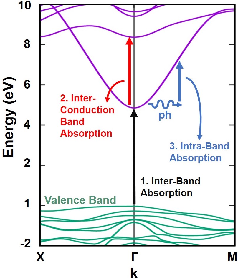
Peelaers et al. recently calculated the optical absorption cross-sections of free electrons from the first-principle electronic bandstructure of Ga2O3, and predicted unique features of both intra- and inter-conduction band transitions Peelaers and Van de Walle (2019, 2017). In this paper, we report results from steady state and ultrafast optical transmission spectroscopy of doped bulk -Ga2O3 substrates, with direct evidence of the predicted intra- and inter-conduction band absorption processes. At the point, the lowest conduction band of -Ga2O3 has Ga:4s symmetry and the next lowest conduction band has Ga:4p symmetry Dong et al. (2017). Inter-conduction band optical absorption between these two bands is therefore possible (see Figure 1). We observe a strong absorption peak near nm (3.55 eV) in doped -Ga2O3 samples, which is absent in undoped or lightly doped samples. This is consistent with the predicted inter-conduction band absorption Peelaers and Van de Walle (2017). This absorption feature is found to depend on the polarization of light, and becomes negligibly small for light polarized along the crystal b-axis ([010]).
Additionally, we observe that the strength of the optical absorption in the entire visible to IR wavelength range varies with the photon frequency , as . This differs from the typical dependence explained by the Drude model for intra-band free-carrier absorption Baker-Finch et al. (2014); von Baltz and Escher (1972). Peelaers et al. predicted that indirect longitudinal optical (LO) phonon mediated intra-band optical transitions in -Ga2O3 should follow this unconventional dependence in the free carrier absorption coefficient in the visible to the near-IR wavelength rangePeelaers and Van de Walle (2019); Peelaers, Kioupakis, and Van de Walle (2012); Peelaers, Kioupakis, and Van de Walle (2019). Our experimental observations confirm this second prediction as well.
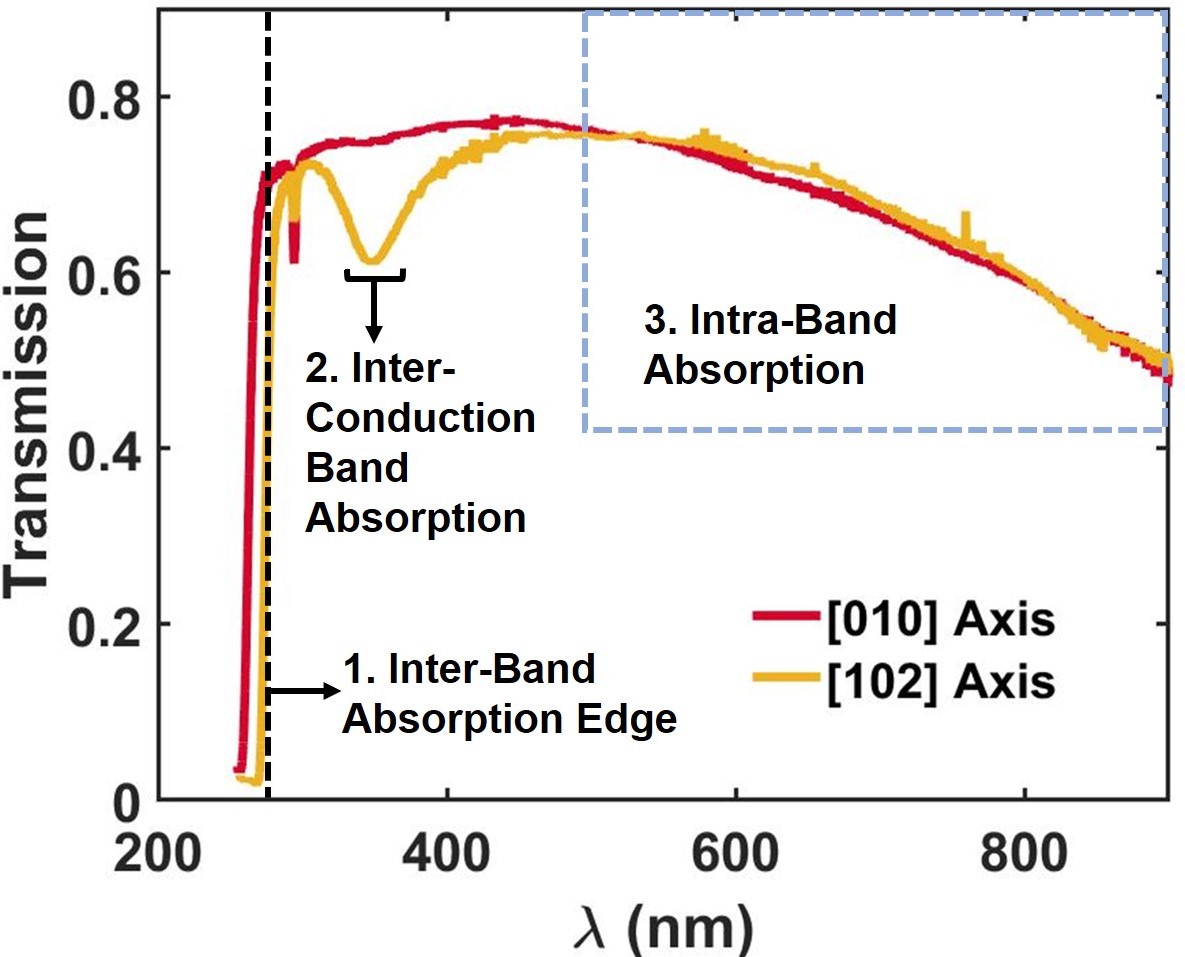
Optical transmission spectroscopy measurements were performed on Sn-doped bulk () -Ga2O3 samples, grown using the edge-defined film-fed growth (EFG) technique by the Tamura Corporation. The sample had a free-electron density of cm-3, and a thickness of m. The optical transmission spectrum was measured at room temperature using light polarized along different crystal axes of -Ga2O3. Figure 2 shows the measured optical transmissivity as a function of the light wavelength for light polarized along the [102] and [010] crystal axes. The valence band to lowest conduction band absorption edge is polarization dependent, and is measured to be at 260 nm (4.77 eV) and 273 nm (4.54 eV) for light polarized along the [010] and [102] axes respectively. This is consistent with what has been observed experimentally and calculated theoretically Ricci et al. (2016); Peelaers and Van de Walle (2017). In addition to the standard optical absorption edge, the transmission spectra in Figure 2 shows two distinct free-carrier absorption features below the bandgap.
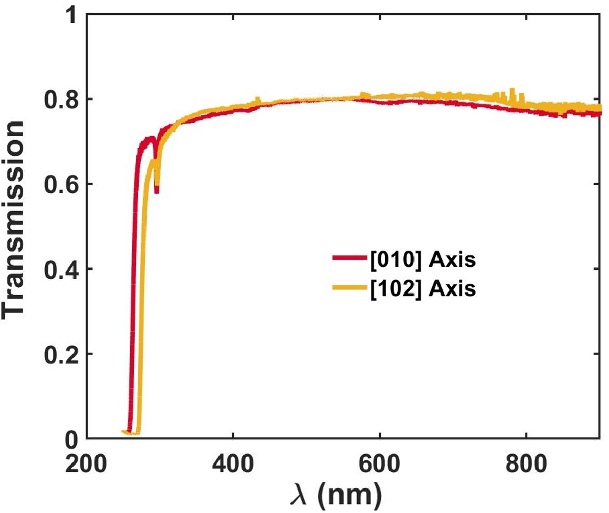
First, broad wavelength-dependent and polarization-independent absorption is observed in the entire visible to near-IR wavelength range. Second, a clear absorption dip is seen around 349 nm. The strength of this absorption was found to be polarization dependent. Measurements performed on undoped samples did not exhibit either of these two absorption features. For example, Figure 3 shows the transmission through a 300 m thick, unintentionally doped ( cm-3), () -Ga2O3 sample (also grown by the Tamura Corporation using the EFG method). This indicates that these two absorption features shown in Figure 2 are due to the presence of free carriers. We attribute the broad wavelength-dependent absorption to intra-conduction band absorption and the absorption dip near 349 nm to inter-conduction band absorption. Note that in addition to the free-carrier absorption described, a sharp absorption feature centered at 296 nm is also seen in the transmission spectrum of both doped and undoped () -Ga2O3 samples (see Figures 2 and 3). While the origin of this absorption is unclear, its presence in both doped and undoped samples suggests that it is not related to doping or to the presence of electrons in the conduction band. In what follows, we first discuss the intra-band absorption spectra and then the inter-conduction band absorption process.
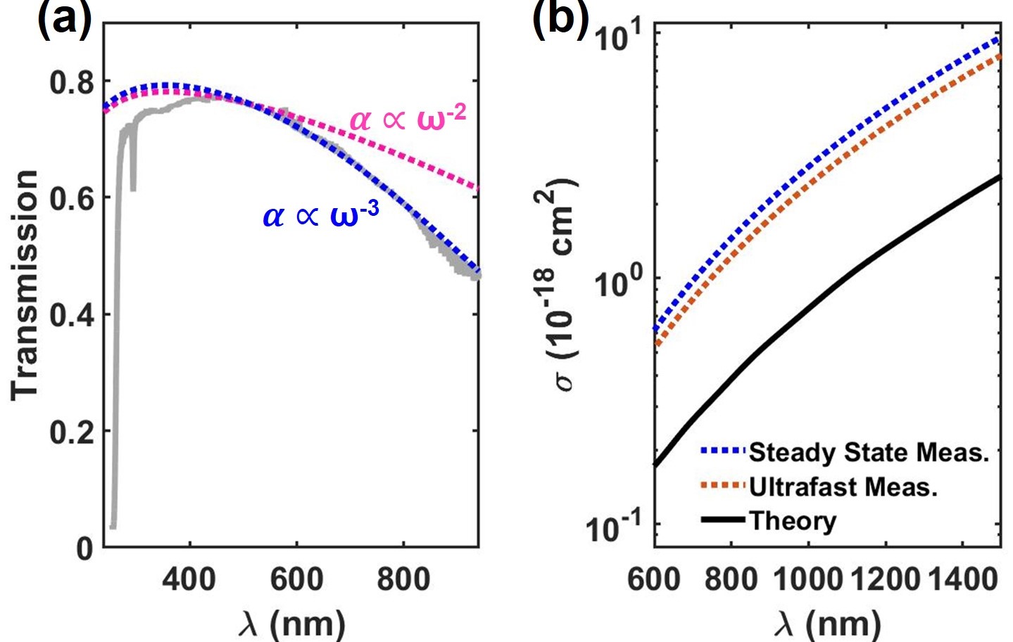
We model light transmissivity through the sample with the simple equation, , where is the light absorption coefficient, is the sample thickness ( m), and is the reflectivity at the two facets of the sample. is calculated using the Fresnel equation assuming normal light incidence at the air - -Ga2O3 interface. Wavelength-dependent values of the measured dielectric tensorSturm et al. (2015) of -Ga2O3 are used to calculate the reflectivity. We then fit the measured transmission spectra (from Figure 2) using absorption coefficients with an inverse power law frequency dependence (i.e. ). Figure 4(a) shows the measured transmission spectrum for light polarized along the [010] axis, along with fits to the data assuming (Drude model) and frequency dependence of the absorption coefficient . As can be seen from this figure, an absorption coefficient fits the measured transmission spectrum well over a broad wavelength range. The observed frequency dependence of the absorption coefficient in our experiments confirms the frequency dependence predicted by theoretical calculations Peelaers and Van de Walle (2019).
Intra-band optical absorption cross-section (calculated by dividing the absorption coefficient with the free electron density) extracted from the transmission measurements and calculated using first principles Peelaers and Van de Walle (2019) are plotted as a function of wavelength in Figure 4(b). Whereas the frequency dependence of the measured and calculated absorption cross-sections agree well, the theoretically calculated cross-section is smaller by a factor of . This difference could be due to multiple reasons. Small differences in the curvature of the calculated bands might lead to an underestimated cross section. Further, the strength of the theoretically calculated electron-phonon coupling might be underestimated. Likely, a combination of the two factors is responsible for the difference.
Despite the difference in the measured and calculated magnitudes, the agreement in wavelength dependence confirms that longitudinal optical (LO) phonon emission is the mechanism behind the momentum conservation in the intra-band light absorption by free electrons in -Ga2O3, in the visible to near-IR wavelength range Peelaers and Van de Walle (2019). This is not unexpected given the large LO phonon-electron coupling strength in -Ga2O3 Ma et al. (2016); Kang et al. (2017); Ghosh and Singisetti (2016); Mengle and Kioupakis (2019). The origin of the (rather than ) dependence of the absorption cross-section can be traced to the fact that far from the point in the -Ga2O3 bandstructure (see Figure 1), the conduction band becomes nearly linear in Peelaers and Van de Walle (2019, 2017). Similar to our observations, this dependence has also been theoretically predicted and experimentally observed in SnO2, another transparent conducting oxide Peelaers, Kioupakis, and Van de Walle (2012); Summitt and Borrelli (1965). Finally, the fact that this intra-band absorption strength does not depend on light polarization is expected given the near isotropy of the lowest conduction band electron states in -Ga2O3 Peelaers and Van de Walle (2015); Kang et al. (2017).
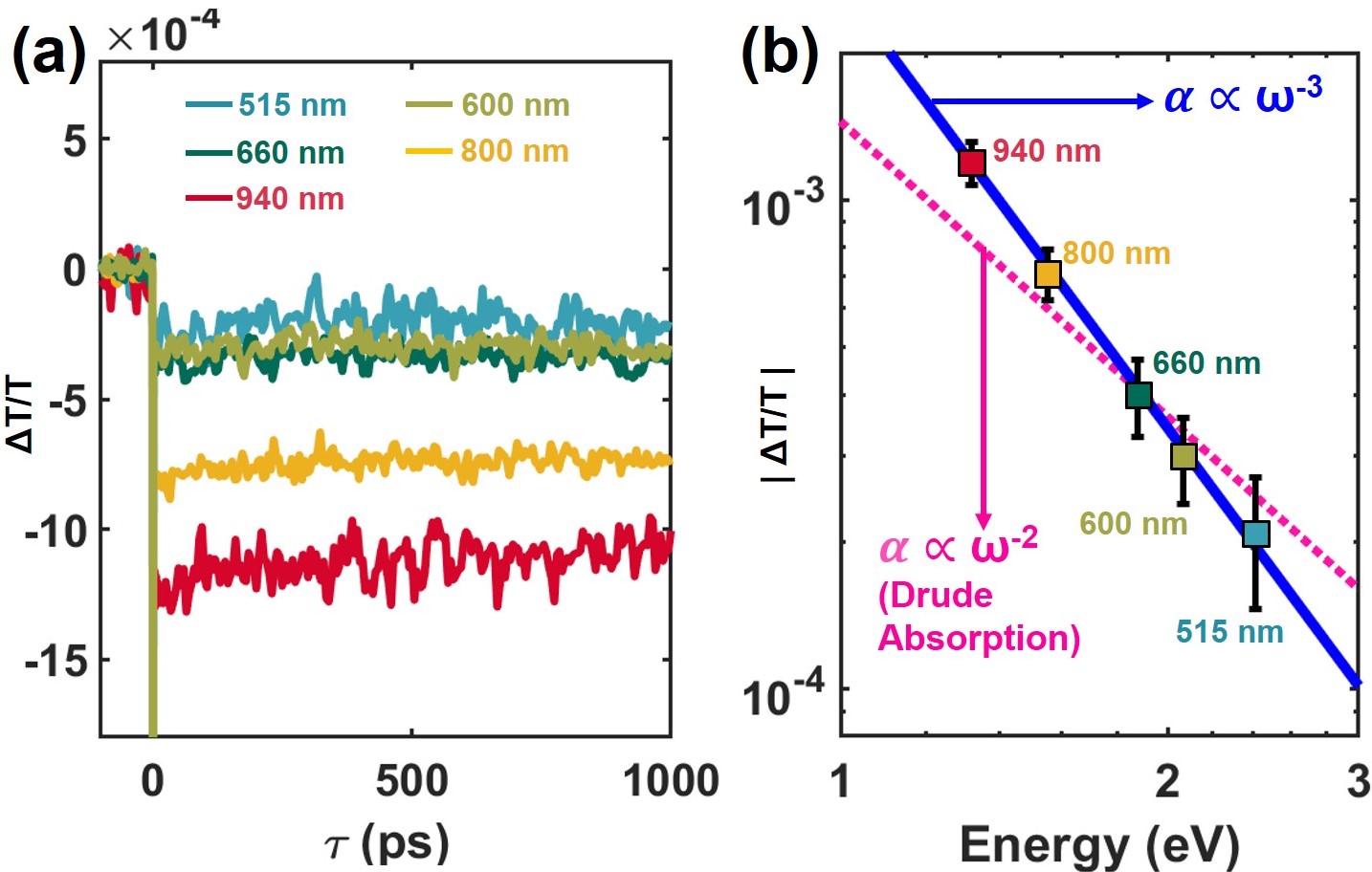
Impurities and defects can affect the measured wavelength dependence of the optical absorption. This is especially true for visible to near-IR absorption in wide bandgap materials. To isolate the optical absorption due to free carriers, it is thus preferable to measure free carrier absorption by modulating the conduction band electron density, and detecting only the resulting changes in the sub-bandgap light absorption. To accomplish this we measured time-resolved transmission through a photoexcited Sn-doped, 450 m thick, bulk () -Ga2O3 sample of free electron concentration cm-3 using ultrafast pump-probe spectroscopy. This sample was also grown using the EFG method by Tamura Corporation. We used a 405 nm center-wavelength ultrafast optical pulse as the pump that excited electrons from the valence band to the conduction band via a two-photon absorption process, as in our previous work Koksal et al. (2018). The center-wavelength of the synchronized probe pulse, polarized along the crystal -axis (orthogonal to the - and -axes), was varied in the visible to the near-IR wavelength range.
Figure 5(a) shows the differential probe transmission () plotted as a function of the probe delay (w.r.t. the pump) for different probe wavelengths. is negative because of optical absorption by photoexcited free electrons. The measured differential transmission magnitudes for different probe wavelengths, for a fixed probe delay ( ps), are plotted as a function of the probe photon energy in Figure 5(b). Also plotted are the best fits for , assuming absorption coefficients with frequency dependence given by and . This figure shows that calculating using fits the data accurately. In addition, as shown in Figure 4(b), the values of the absorption cross-section extracted from ultrafast measurements are in excellent agreement with those obtained using steady state transmission experiments.
We now consider the inter-conduction band absorption features seen in Figure 2. This absorption is centered at nm (3.55 eV), and is polarization dependent. The largest absorption is seen for light polarized along the [102] axis. For light polarized along the orthogonal [010] axis, the inter-conduction band absorption is much weaker. As shown in Fig. 1 this absorption is due to transitions occurring between the lowest (partially filled) conduction band and the next conduction band, whose energy difference determines the optical absorption wavelength. The magnitude of the absorption depends on the dipole transition matrix elements, which are polarization dependent. According to the first-principles calculation of the bandstructure Peelaers and Van de Walle (2017), the inter-conduction band absorption for light polarized along the [010] axis should be much smaller than the absorption for light polarized along the [102] axis, which is in agreement with the experimental observation.
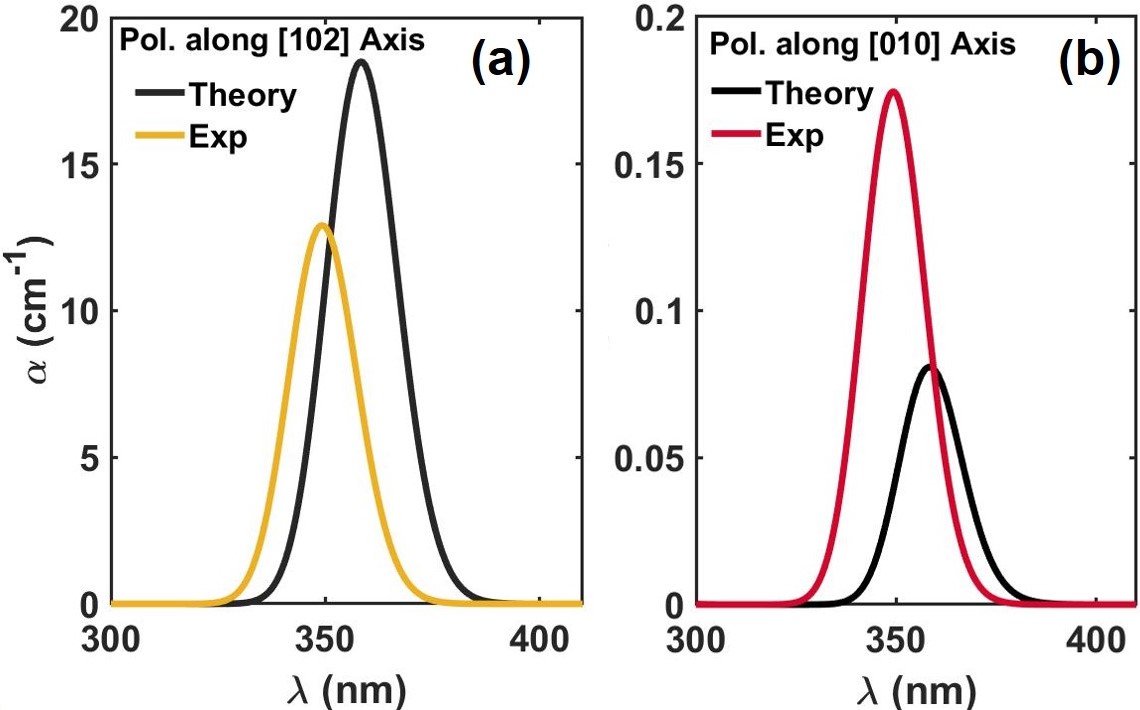
After subtracting a relatively small but broadband absorption (partly due to intra-conduction band absorption), a Gaussian lineshape was used to fit the inter-conduction band absorption dips for light polarized along the [102] and [010] axes. Figure 6 shows the spectra of the inter-conduction band absorption coefficients extracted using this method, along with the theoretically calculated spectra from first principles Peelaers and Van de Walle (2017). For light polarization along the [102] and [010] axes, the experimental absorption coefficient values peak at cm-1 and cm-1, respectively. The agreement between experiments and theory is remarkable. The difference in the center wavelength of the absorption, between measurements and calculations, for both polarization directions is less than 10 nm (96 meV). This is well within the expected accuracy of the calculations. The difference in the peak absorption between measurement and theory is around 26% for light polarization along the [102] axis, which is not unexpected given the experimental procedure used to extract the inter-conduction band absorption coefficient. The difference in the peak absorption between measurement and theory is larger for light polarization along the [010] axis; the measured absorption peak is almost twice as large as that predicted by theory. We should point out here that the peak absorption for light polarization along the [010] axis is extremely small (two orders of magnitude weaker than the absorption for light polarization along the [102] axis), and the observed dip in the transmission spectrum (Figure 2) is at the threshold of the signal to noise ratio available in our experimental setup. Therefore, a greater error would not be unexpected in quantifying the value of the absorption coefficient for light polarization along the [010] axis.
In conclusion, we have presented detailed experimental evidence of intra- and inter-conduction band optical absorption processes by free electrons in the conduction band of the ultra-wide bandgap semiconductor -Ga2O3. Two unique features of this semiconductor were recently predicted by theoretical calculations: (1) sub-bandgap optical transitions in the UV from the bottom of the conduction band to the next conduction band with absorption coefficients in the cm-1 range, and (2) an intra-conduction band transition that goes as . Both these optical transitions are experimentally observed to be qualitatively and quantitatively consistent with the predictions. Since both the studied absorption mechanisms involve free electrons in the conduction band, a larger electron density would result in greater light absorption and reduced transparency in the UV, Visible, and Near-IR wavelength range. This is thus important to take into account in the design of optoelectronic devices relying on a high degree of transparency. Further, electrons in the lowest conduction band states can scatter into the higher conduction band under high electric fields, and the absorption measurements provide a measure of the matrix elements for such transitions.
Acknowledgements.
*Singh and Koksal contributed equally to this work. This work was supported by NSF under Grant No. DMR-1719875 and AFOSR under Grant No. FA9550-17-1-0048.Data Availability Statement
The data that support the findings of this study are available from the corresponding author upon reasonable request.
References
- Ricci et al. (2016) F. Ricci, F. Boschi, A. Baraldi, A. Filippetti, M. Higashiwaki, A. Kuramata, V. Fiorentini, and R. Fornari, Journal of Physics: Condensed Matter 28, 224005 (2016).
- Orita et al. (2000) M. Orita, H. Ohta, M. Hirano, and H. Hosono, Applied Physics Letters 77, 4166–4168 (2000).
- Matsumoto et al. (1974) T. Matsumoto, M. Aoki, A. Kinoshita, and T. Aono, Japanese Journal of Applied Physics 13, 1578–1582 (1974).
- Tippins (1965) H. H. Tippins, Phys. Rev. 140, A316–A319 (1965).
- Aida et al. (2008) H. Aida, K. Nishiguchi, H. Takeda, N. Aota, K. Sunakawa, and Y. Yaguchi, Japanese Journal of Applied Physics 47, 8506–8509 (2008).
- Kuramata et al. (2016) A. Kuramata, K. Koshi, S. Watanabe, Y. Yamaoka, T. Masui, and S. Yamakoshi, Japanese Journal of Applied Physics 55, 1202A2 (2016).
- Galazka et al. (2014) Z. Galazka, K. Irmscher, R. Uecker, R. Bertram, M. Pietsch, A. Kwasniewski, M. Naumann, T. Schulz, R. Schewski, D. Klimm, and M. Bickermann, Journal of Crystal Growth 404, 184–191 (2014).
- Hu et al. (2015) G. C. Hu, C. X. Shan, N. Zhang, M. M. Jiang, S. P. Wang, and D. Z. Shen, Opt. Express 23, 13554–13561 (2015).
- Ji et al. (2006) Z. Ji, J. Du, J. Fan, and W. Wang, Optical Materials 28, 415 – 417 (2006).
- Oshima, Okuno, and Fujita (2007) T. Oshima, T. Okuno, and S. Fujita, Japanese Journal of Applied Physics 46, 7217–7220 (2007).
- Minami, Nishi, and Miyata (2013) T. Minami, Y. Nishi, and T. Miyata, Applied Physics Express 6, 044101 (2013).
- Haga and Kimura (1964) E. Haga and H. Kimura, Journal of the Physical Society of Japan 19, 1596–1606 (1964).
- Glosser, Fischer, and Seraphin (1970) R. Glosser, J. E. Fischer, and B. O. Seraphin, Phys. Rev. B 1, 1607–1610 (1970).
- Balkanski, Aziza, and Amzallag (1969) M. Balkanski, A. Aziza, and E. Amzallag, physica status solidi (b) 31, 323–330 (1969).
- Canestraro et al. (2008) C. D. Canestraro, M. M. Oliveira, R. Valaski, M. V. da Silva, D. G. David, I. Pepe, A. F. da Silva, L. S. Roman, and C. Persson, Applied Surface Science 255, 1874 – 1879 (2008).
- Baker-Finch et al. (2014) S. C. Baker-Finch, K. R. McIntosh, D. Yan, K. C. Fong, and T. C. Kho, Journal of Applied Physics 116, 063106 (2014).
- Perkowitz (1969) S. Perkowitz, Journal of Applied Physics 40, 3751–3754 (1969).
- Perkowitz (1971) S. Perkowitz, Journal of Physics and Chemistry of Solids 32, 2267 – 2274 (1971).
- von Baltz and Escher (1972) R. von Baltz and W. Escher, physica status solidi (b) 51, 499–507 (1972).
- Peelaers, Kioupakis, and Van de Walle (2012) H. Peelaers, E. Kioupakis, and C. G. Van de Walle, Applied Physics Letters 100, 011914 (2012).
- Peelaers and Van de Walle (2019) H. Peelaers and C. G. Van de Walle, Phys. Rev. B 100, 081202 (2019).
- Peelaers and Van de Walle (2017) H. Peelaers and C. G. Van de Walle, Applied Physics Letters 111, 182104 (2017).
- Dong et al. (2017) L. Dong, R. Jia, B. Xin, B. Peng, and Y. Zhang, Scientific Reports 7, 40160 (2017).
- Peelaers, Kioupakis, and Van de Walle (2019) H. Peelaers, E. Kioupakis, and C. G. Van de Walle, Applied Physics Letters 115, 082105 (2019).
- Sturm et al. (2015) C. Sturm, J. Furthmüller, F. Bechstedt, R. Schmidt-Grund, and M. Grundmann, APL Materials 3, 106106 (2015).
- Ma et al. (2016) N. Ma, N. Tanen, A. Verma, Z. Guo, T. Luo, H. G. Xing, and D. Jena, Applied Physics Letters 109, 212101 (2016).
- Kang et al. (2017) Y. Kang, K. Krishnaswamy, H. Peelaers, and C. G. Van de Walle, Journal of Physics: Condensed Matter 29, 234001–234001 (2017).
- Ghosh and Singisetti (2016) K. Ghosh and U. Singisetti, Applied Physics Letters 109, 072102 (2016).
- Mengle and Kioupakis (2019) K. A. Mengle and E. Kioupakis, AIP Advances 9, 015313 (2019).
- Summitt and Borrelli (1965) R. Summitt and N. Borrelli, Journal of Physics and Chemistry of Solids 26, 921 – 925 (1965).
- Peelaers and Van de Walle (2015) H. Peelaers and C. G. Van de Walle, physica status solidi (b) 252, 828–832 (2015).
- Koksal et al. (2018) O. Koksal, N. Tanen, D. Jena, H. G. Xing, and F. Rana, Applied Physics Letters 113, 252102 (2018).