Ultra-large actively tunable photonic band gaps
via plasmon-analog of index enhancement
Abstract
We present a novel method for active continuous-tuning of a band gap which has a great potential to revolutionalize current photonic technologies. We study a periodic structure of x and y-aligned nanorod dimers. Refractive index of a y-polarized probe pulse can be continuously-tuned by the intensity of an x-polarized auxiliary (pump) pulse. Order of magnitude index-tuning can be achieved with a vanishing loss using the plasmon-analog of refractive index enhancement [PRB 100, 075427 (2019)]. Thus, a large band gap can be created from a non-existing gap via the auxiliary pulse. We also present a “proof of principle” demonstration of the phenomenon using numerical solutions of Maxwell equations. The new method, working for any crystal dimensions, can also be utilized as a linear photonic switch operating at tens of femtoseconds.
Ability of crafting materials at dimensions comparable to wavelength of light not only allowed control of electromagnetic radiation at nanoscale, but also made development of metamaterials Liu and Zhang (2011), such as photonic crystals (PCs) Yablonovitch (1987); Yablonovitch et al. (1991); Wijnhoven and Vos (1998), possible. PCs, periodically altering refractive index materials, reshape the propagation (dispersion) of the incident light and even can forbid it at certain propagation directions within some frequency ranges, named as photonic band gaps (PBGs) Leistikow et al. (2011). PBGs, whose structure depends on the periodicity and index contrast, can be utilized as waveguides Knight et al. (1996), optical cavities Akahane et al. (2003), optical memories Kuramochi et al. (2014) and switches Euser et al. (2007); Yüce et al. (2013). This way PBGs enable on-chip photonic signal processing Wang and Long (2018). These structures enable control even over quantum phenomena Haroche and Kleppner (1989); Lodahl et al. (2004); Madsen et al. (2011) such as spontaneous emission Scully (2015); Scully and Svidzinsky (2009) and entanglement Tasgin (2017) at nanoscale.
A conventional PC —whose PBG structure remains fixed after manufacturing— cannot operate, e.g., as a switch, although it is useful for photonic waveguide and cavity applications. External control of the constituent material’s refractive index, however, demonstrated to tune the PBG width about a few percent which allows the utilization of PCs as photonic switches. Refractive index of semiconductors (materials commonly employed in current PC technologies owing to their relatively-high index, =3.5-4, and small absorption) can be tuned externally (actively) via optical heating Reed and Knights (2004), free-carrier excitation Almeida et al. (2004) and electronic Kerr-effect Ctistis et al. (2011); Yüce et al. (2013). While technique of free-carrier excitation provides the largest index change (3%), its response time (tens of picoseconds) is much longer compared to the modulation time of the Kerr effect (a few femtosecond). Using the Kerr effect, in contrast, achievable index change is only 1%.
Metal nanostructures, which can localize the incident light into nm-sized hotspots, are also utilized for photonic technologies. Hybrid metastructures, created with semiconductors and metallic nanostructures, increase the versatility of integrated photonic structures Fan and Padilla (2015); He et al. (2019); Kang et al. (2019). Yet, regarding the modulation depth, response time and (especially) metal-induced losses their functionalities are limited Fan and Padilla (2015); He et al. (2019); Kang et al. (2019).
Therefore, a mechanism providing; (i) a large refractive index change (ii) minimal loss, and (iii) a short response time will revolutionalize the dynamic control of light on-a-chip. Fortunately, in this paper, we propose the utilization of a recently-discovered extraordinary index enhancement (linear control) scheme for achieving a game-changing control over the PGBs of a PC. Actually, utilization of index enhancement Scully and Zubairy (1997); Fleischhauer et al. (2005) as PCs has already been studied in cold atoms Taşgın et al. (2007); Müstecaplıoğlu and Oktel (2005).
We utilize a recently explored phenomenon: plasmon-analog of index enhancement Panahpour et al. (2019). Lavrinenko and colleagues Panahpour et al. (2019) demonstrate that polarization response of a y-aligned silver nanorod to a y-polarized probe pulse can be controlled by the presence of an x-polarized auxiliary pulse, see Fig. 1. Owing to the shape resonance (selective coupling Andrews et al. (2019)) of nanorods; x,y-polarized pulse can excite “only” the x,y-aligned nanorods, respectively. Beyond studying the enhancement using a basic analytical model, which has widely been demonstrated to work very well for plasmonic path interference effects Wu et al. (2010); Lovera et al. (2013); Taşgın et al. (2018), Lavrinenko and colleagues also demonstrated the phenomenon via numerical solutions of 3D Maxwell equations. This scheme not only enhances the refractive index more than 2-orders of magnitude, but also results a canceled absorption at the enhancement frequency —just as the same in its EIT counterpart Fleischhauer et al. (2005). This phenomenon allows us to adjust the “loss-free” refractive index of metamaterials without sacrificing the probe signal to metallic losses.
In this paper, we show that plasmonic index enhancement is the dream-spouse for a photonic crystal. While other methods Reed and Knights (2004); Almeida et al. (2004); Ctistis et al. (2011); Yüce et al. (2013) can tune the band gap size only about 2-3%, the presented scheme can create a large (e.g. 0.3 and 0.5 eV in Fig. 3) from a nonexisting gap only with an extremely small filling ratio PSf . One can achieve “any particular value” of the band gap width between 0-0.3 eV for a y-polarized probe pulse () by merely arranging the intensity () of the x-polarized auxiliary (pump) pulse between =0-10, working in the low intensity regime. is the intensity of the weak probe field. Moreover, response time is limited with the plasmon lifetime ( fs Zoric et al. (2011)) and relaxation time as the scheme utilizes metal nanoparticles. In the case of silver nanorods, Ref. Panahpour et al. (2019) originally studies, a 100 fs linear photonic switching can be achieved using 30 fs auxiliary pulse, see Fig. 5, where silver’s plasmon lifetime we use is already 40 fs long. It is apparent that using a smaller plasmon lifetime material, such as platinum Zoric et al. (2011); Yildiz et al. (2020), should result much faster switching times PSl .
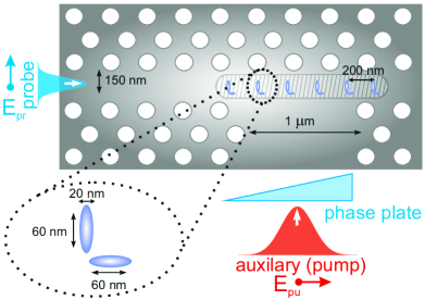
Owing to the supreme index enhancement, PBG effects show up, see Figs. 3 and 4, via 6 dimer layers. This helps the miniaturization of PCs. The sample setup, Fig. 1, presents a 750 nm long enhanced photonic crystal on a PC-waveguide chip employing CMOS-compatible noble metal (silver) materials.
We also present a demonstration of the phenomenon via numerical solutions of Maxwell equations (Fig. 4). We kindly remark that our aim, in this prominent work, is merely presenting the first study for the utilization of plasmon index enhancement for PBG structures operating at room temperature.
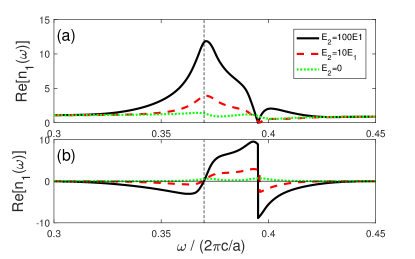
Index-enhancement scheme.— Fig. 1 demonstrates a sample setup for implementing index-enhancement phenomenon for on-chip photonic operations. 6 layers of silver nanorod dimers (see the inset) switches the transmission of a -polarized probe pulse () of frequency via an x-polarized auxiliary (pump) pulse (). When the auxiliary pulse is off, the refractive index of sized () nanorods becomes exceedingly small for a density of 1 dimer in volume =200150200 . Here 200 nm is the periodicity and 150200 corresponds to width and depth of the cavity in which silver dimers are placed PSn . We note that these are rough calculations. Filling ratio of the index-enhanced layer, a single dimer in each one, is 0.1%. Thus, probe is transmitted with a relatively small absorption, i.e., 35%. (Probe can be transmitted without any absorption as well, see below.) When the auxiliary pulse is turned on, with amplitudes and , however, effective refractive index of the thin layers (10 nm length) is enhanced dramatically, see Fig. 2a, thus turning ON a PBG of width 0.3 eV and 0.5 eV, respectively. See Fig 3. The x-polarized auxiliary pulse couples only to the x-aligned silver nanorod. The x-aligned nanorod affects the response of the y-aligned nanorod via a coupling through the hotspot appearing at the intersection of the two orthogonal rods. When the auxiliary pulse is present, y-polarized nanorod gives different polarization responses () for different values of the probe field .
Dynamics of such a coupled system can be described by a basic model Panahpour et al. (2019); Postaci et al. (2018)
| (1) | |||
| (2) |
which is very successful in demonstrating the Fano-like path-interference effects in plasmonic nanostructures Wu et al. (2010); Lovera et al. (2013); Taşgın et al. (2018). Simulations in Ref. Panahpour et al. (2019) and the FEM simulations we carry out here, also demonstrate the appearance of the phenomenon. , and Panahpour et al. (2019) are the damping rates, resonances and the coupling between the two plasmon oscillations of the two nanorod, respectively. is the resonance of both nanorods. Here, only is different from the one of Ref. Panahpour et al. (2019) since we determine the damping rates of nanorods from experimental dielectric function of silver. Actually, such a tidy choice of parameters is not necessary for this initial work which aims to present the implementation of the phenomenon for photonic technologies.
For a monochromatic auxiliary pulse , of the same frequency with the probe, the numerical solution for the susceptibility of the medium
| (3) |
can be obtained Panahpour et al. (2019); Postaci et al. (2018). . The dimensionless oscillator strength is determined by setting nonenhanced susceptibility Postaci et al. (2018) to , with is the polarization density calculated for ellipsoid nanorods Panahpour et al. (2019); Bohren and Huffman (2008); Postaci et al. (2018), for 1 dimer in index-enhanced layer (20 nm), with volume =20150200 in Fig. 1.
Since the auxiliary field, in our case an ultrashort pulse, has a broad frequency band, we take pulse unlike Ref. Panahpour et al. (2019). We solve Eqs. (1-2) in the frequency domain for the Gaussian auxiliary pulse. . Fig. 2 plots the real and imaginary parts of the enhanced index PSi for , and . We note that a double resonance for appears, because coupling between the two nanorods exists when the auxiliary pulse is turned off.
In Fig. 2b, we observe that imaginary part of the index becomes zero almost at the same frequency (vertical dashed-line) for and , where the index becomes superiorly enhanced.
The phase plate.— Setup in Fig. 1 includes a critical apparatus; a phase plate. Eq. (3) shows that the phase-difference between the auxiliary and probe pulse, , plays an important role for the index enhancement to appear. The aux-probe phase-differences for the first and second dimer are not the same, since the probe does not have the same phase at different dimers (x-positions). Hence, when the first dimer is set to enhanced index (for y-polarized probe), the second dimer can possess a non-enhanced index; destroying the periodicity. Thus, we rephase the front of the auxiliary pulse with a phase plate either in the entrance of the aux port of the waveguide, or in front of (or inside) the auxiliary source. Such a necessity for phase-tuning, most probably, is the reason large PBG changes cannot be observe in experiments with periodic nanoparticles Fan and Padilla (2015); He et al. (2019); Kang et al. (2019).
Photonic band gap.— In Fig. 3, we present the transmission for a 6-layer index-enhanced PC of dimers with periodicity =200 nm. It is striking that: while there exists a large amount of gain in the left of in Fig. 2b, Fig. 3 shows that PGB, the 6-layer enhanced PC creates, can turn-OFF the transmission in a wide frequency region both for and . We note that, in the figures we scale the frequencies by and momentum-vector by . In determining the natural band gap region, we first calculate the band diagram for the constant index , then we choose periodicity accordingly as performed in Ref. Taşgın et al. (2007).
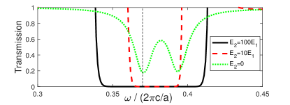
We also calculate the photonic band structure where a similar order for the transmission appears. is the imaginary part of the wavevector-solution at 0.37.
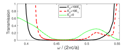
Numerical Solutions of Maxwell’s Equations.— We also perform FEM (frequency domain) simulations using COMSOL as a proof of principle demonstration of the phenomenon. First, we obtain the y-component of the susceptibility by simulating the response of a single dimer which is coupled to the probe and auxiliary fields whose phases differ by /2. We assume that the y-component of the electric field response of the dimer is directly proportional to the y-component of susceptibility. We acquire the refractive index that has a similar form with the theoretical results depicted in Fig. 2. Then, we input the calculated index values back to 10 y-aligned nanoparticles separated by the lattice parameter . Transmission properties of the system is depicted in Fig. 4. The value is determined independently from the theoretical calculations PSS : we tested values from 150 nm to 300 nm. We chose such that the PBG matches the index enhancement frequency.
There exist one challenging situation FEM simulations made us realize. The probe field decays after each layer while propagating through the PC. This changes the ratio, hence, the periodicity of the refractive index. In such a setup while PBG effects are still clearly visible, high modulation depths may not be achieved. For circumventing this issue, we propose using another auxiliary wave. An x-polarized (additional) auxiliary wave illuminates the dimers along the z-axis PSz with . This way, creates an unchanged field along x-direction. This is also compatible with our simulations.
We were compelled to proceed with the 2-step approach, described above, in stead of simulating 10-dimers PC in a single step with the auxiliary fields. As the auxiliary pulse intensities would be much larger than the probe intensity, any remnant of aux fields reflected/diffracted at the simulation boundaries do interfere with the probe field com ; PSF . This severely complicates the simulation. Our approach, advantageously, is not vulnerable against such complications.
PC operation regimes.— There can be several options for the operation regions in utilizing the system as a photonic switch. (a) PC can be operated at , but transmission in the switch-on mode drops to 0.15 for this regime, see Fig. 3a. (b) One can choose a better switch-on transmission 0.55 for , since absorption in the switch-off mode is not important for this application. (c) Index-enhancement scheme is an active medium. It displays a substantial gain, e.g., between =0.35-0.37, when the auxiliary (pump) field is set to . Thus, working, for instance, enhances the transmitted pulse several orders of magnitude for via gain, but, suppresses the transmission when auxiliary is turned to due to the band gap. While we demonstrate the switch mechanism for quite different values of the auxiliary field, i.e., and , an optimization can be carried out for smaller differences.
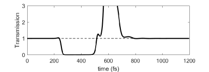
Response time.— In Fig. 5, we present the time development of the transmitted pulse when a 40 fs, auxiliary pulse passes through the enhanced PC. We observe that, although the temporal width of the auxiliary pulse is 40 fs PBG remains off for about 200 fs. This limitation, actually, occurs due to two transient times. The decay time of the surface plasmon oscillations on silver, used in this work Panahpour et al. (2019); Postaci et al. (2018), is already about 40 fs. The switch time is also determined by the relaxation time, appearing due to the interaction between the two nanorods PSt . After 600 fs, we observe the gain amplification of the transmission (it reaches ) during the PBG off regime. This transient also lasts 200 fs, but, increases the modulation depth between 400 fs and 600 fs dramatically. When, for instance, platinum nanorods, of decay time 1 fs are used in the enhanced PC, much faster response times can be achieved. We remark that, a larger damping rate necessitates also a larger coupling for enhancement scheme to appear.
Periodicity on 2D and 3D.— Index enhancement scheme depends critically on the phase difference between the probe and the auxiliary pulses. When there is periodicity of nanodimers along the z-axis in Fig. 1, there would appear no problem. Because, the phase of the auxiliary pulse is constant in the x-z plane. On working the periodicity along the propagation direction of the auxiliary pulse, y, however, one needs to take care of the different positions (so phases) of adjacent dimer arrays along the y-direction. Traveling along the y-directions, the first and the second dimer arrays show different phase-differences for the auxiliary and probe pulses. Index enhancement scheme can be different, even be demolished, in this case. This problem, however, can be circumvented in two ways. (i) One can choose the y-periodicity of the PC such that at a desired operation wavelength altering phases, and , overlap. (ii) A second approach: one could induce an appropriate phase dilation also in the probe field along the y-axis either in the waveguide input or just before PC input. One important point to stress is that in the enhancement scheme, index can be superiorly strengthened such that a single dimer array becomes sufficient for switching operations.
In summary, we show that recently-explored index enhancement for plasmonic nanoparticles Panahpour et al. (2019) can be utilized in photonic crystal technologies for achieving 100% PBG tuning. This is because, available adjustment of refractive index, using this scheme Panahpour et al. (2019), is incomparably larger than the currently applied methods Reed and Knights (2004); Almeida et al. (2004); Ctistis et al. (2011); Yüce et al. (2013). Index enhancement, achieved with a “vanishing loss”, is such a large value (as in its EIT-counterpart Taşgın et al. (2007); Müstecaplıoğlu and Oktel (2005); Fleischhauer et al. (1992)) that using very small filling ratio for nanoparticles becomes sufficient. We also provide a proof of principle demonstration of the phenomenon via numerical solutions of Maxwell equations.
Switching time of the PBG is determined by the decay rate of the metal nanoparticles, so, it is in the femtosecond regime. The gain nature enhances the modulation of the transmission. Vanishing loss at the enhancement frequency can be utilized as undamped switchable cavities at specific frequencies important for quantum optics (information) applications Reiserer and Rempe (2015); Scully et al. (2003); Hardal and Müstecaplıoğlu (2015); Zou et al. (2017).
Therefore, implementation of the plasmon-analog of refractive index enhancement (control) to photonic crystals provides a revolutionary instrument for photonic applications.
Acknowledgements.
The FEM simulations are conducted solely by AKD, sophomore at Bilkent University. MET acknowledges support from TUBA GEBIP 2017 and TUBITAK 1001 No:117F118. AB and MET acknowledge support from TUBITAK 1001 No: 119F101.References
- Liu and Zhang (2011) Yongmin Liu and Xiang Zhang, “Metamaterials: a new frontier of science and technology,” Chemical Society Reviews 40, 2494–2507 (2011).
- Yablonovitch (1987) Eli Yablonovitch, “Inhibited spontaneous emission in solid-state physics and electronics,” Physical Review Letters 58, 2059 (1987).
- Yablonovitch et al. (1991) Eli Yablonovitch, TJ Gmitter, and Kok-Ming Leung, “Photonic band structure: The face-centered-cubic case employing nonspherical atoms,” Physical Review Letters 67, 2295 (1991).
- Wijnhoven and Vos (1998) J. E. G. J. Wijnhoven and W. L. Vos, “Preparation of photonic crystals made of air spheres in titania,” Science 281, 802–804 (1998).
- Leistikow et al. (2011) M. D. Leistikow, A. P. Mosk, E. Yeganegi, S. R. Huisman, A. Lagendijk, and W. L. Vos, “Inhibited spontaneous emission of quantum dots observed in a 3D photonic band gap,” Phys. Rev. Lett. 107, 193903–1–5 (2011).
- Knight et al. (1996) JC Knight, TA Birks, P St J Russell, and DM Atkin, “All-silica single-mode optical fiber with photonic crystal cladding,” Optics Letters 21, 1547–1549 (1996).
- Akahane et al. (2003) Yoshihiro Akahane, Takashi Asano, Bong-Shik Song, and Susumu Noda, “High-q photonic nanocavity in a two-dimensional photonic crystal,” Nature 425, 944–947 (2003).
- Kuramochi et al. (2014) Eiichi Kuramochi, Kengo Nozaki, Akihiko Shinya, Koji Takeda, Tomonari Sato, Shinji Matsuo, Hideaki Taniyama, Hisashi Sumikura, and Masaya Notomi, “Large-scale integration of wavelength-addressable all-optical memories on a photonic crystal chip,” Nature Photon. 8, 474–481 (2014).
- Euser et al. (2007) Tijmen G Euser, Hong Wei, Jeroen Kalkman, Yoonho Jun, Albert Polman, David J Norris, and Willem L Vos, “Ultrafast optical switching of three-dimensional si inverse opal photonic band gap crystals,” Journal of Applied Physics 102, 053111 (2007).
- Yüce et al. (2013) Emre Yüce, Georgios Ctistis, Julien Claudon, Emmanuel Dupuy, Robin D Buijs, Bob de Ronde, Allard P Mosk, Jean-Michel Gérard, and Willem L Vos, “All-optical switching of a microcavity repeated at terahertz rates,” Optics Letters 38, 374–376 (2013).
- Wang and Long (2018) Jian Wang and Yun Long, “On-chip silicon photonic signaling and processing: a review,” Science Bulletin 63, 1267–1310 (2018).
- Haroche and Kleppner (1989) Serge Haroche and Daniel Kleppner, “Cavity quantum electrodynamics,” Phys. Today 42, 24–30 (1989).
- Lodahl et al. (2004) Peter Lodahl, A Floris Van Driel, Ivan S Nikolaev, Arie Irman, Karin Overgaag, Daniël Vanmaekelbergh, and Willem L Vos, “Controlling the dynamics of spontaneous emission from quantum dots by photonic crystals,” Nature 430, 654–657 (2004).
- Madsen et al. (2011) Kristian Høeg Madsen, Serkan Ates, Toke Lund-Hansen, A Löffler, S Reitzenstein, A Forchel, and Peter Lodahl, “Observation of non-markovian dynamics of a single quantum dot in a micropillar cavity,” Physical Review Letters 106, 233601 (2011).
- Scully (2015) Marlan O Scully, “Single photon subradiance: quantum control of spontaneous emission and ultrafast readout,” Physical Review Letters 115, 243602 (2015).
- Scully and Svidzinsky (2009) Marlan O Scully and Anatoly A Svidzinsky, “The super of superradiance,” Science 325, 1510–1511 (2009).
- Tasgin (2017) Mehmet Emre Tasgin, “Many-particle entanglement criterion for superradiantlike states,” Physical Review Letters 119, 033601 (2017).
- Reed and Knights (2004) Graham T Reed and Andrew P Knights, Silicon photonics: an introduction (John Wiley & Sons, 2004).
- Almeida et al. (2004) Vilson R Almeida, Carlos A Barrios, Roberto R Panepucci, and Michal Lipson, “All-optical control of light on a silicon chip,” Nature 431, 1081–1084 (2004).
- Ctistis et al. (2011) Georgios Ctistis, Emre Yuce, Alex Hartsuiker, Julien Claudon, Maela Bazin, Jean-Michel Gérard, and Willem L Vos, “Ultimate fast optical switching of a planar microcavity in the telecom wavelength range,” Applied Physics Letters 98, 161114 (2011).
- Fan and Padilla (2015) Kebin Fan and Willie J Padilla, “Dynamic electromagnetic metamaterials,” Materials Today 18, 39–50 (2015).
- He et al. (2019) Qiong He, Shulin Sun, Lei Zhou, et al., “Tunable/reconfigurable metasurfaces: Physics and applications,” Research 2019, 1849272 (2019).
- Kang et al. (2019) Lei Kang, Ronald P Jenkins, and Douglas H Werner, “Recent progress in active optical metasurfaces,” Advanced Optical Materials 7, 1801813 (2019).
- Scully and Zubairy (1997) M. O. Scully and M. S. Zubairy, Quantum Optics (Cambridge University Press, New York, 1997).
- Fleischhauer et al. (2005) Michael Fleischhauer, Atac Imamoglu, and Jonathan P Marangos, “Electromagnetically induced transparency: Optics in coherent media,” Reviews of Modern Physics 77, 633 (2005).
- Taşgın et al. (2007) Mehmet Emre Taşgın, Özgür Esat Müstecaplıoğlu, and MÖ Oktel, “Photonic band gap in the triangular lattice of bose-einstein-condensate vortices,” Physical Review A 75, 063627 (2007).
- Müstecaplıoğlu and Oktel (2005) ÖE Müstecaplıoğlu and MÖ Oktel, “Photonic band gap via quantum coherence in vortex lattices of bose-einstein condensates,” Physical Review Letters 94, 220404 (2005).
- Panahpour et al. (2019) Ali Panahpour, Abolfazl Mahmoodpoor, and Andrei V Lavrinenko, “Refraction enhancement in plasmonics by coherent control of plasmon resonances,” Physical Review B 100, 075427 (2019).
- Andrews et al. (2019) David Andrews, Thomas Nann, and Robert H Lipson, Comprehensive nanoscience and nanotechnology (Academic Press, 2019).
- Wu et al. (2010) Xiaohua Wu, Stephen K Gray, and Matthew Pelton, “Quantum-dot-induced transparency in a nanoscale plasmonic resonator,” Optics express 18, 23633–23645 (2010).
- Lovera et al. (2013) Andrea Lovera, Benjamin Gallinet, Peter Nordlander, and Olivier JF Martin, “Mechanisms of fano resonances in coupled plasmonic systems,” ACS Nano 7, 4527–4536 (2013).
- Taşgın et al. (2018) Mehmet Emre Taşgın, Alpan Bek, and Selen Postacı, “Fano resonances in the linear and nonlinear plasmonic response,” in Fano Resonances in Optics and Microwaves (Springer, 2018) pp. 1–31.
- (33) Filling ratio of a silver dimer in Fig. 1 is 0.1%.
- Zoric et al. (2011) Igor Zoric, Michael Zach, Bengt Kasemo, and Christoph Langhammer, “Gold, platinum, and aluminum nanodisk plasmons: material independence, subradiance, and damping mechanisms,” ACS Nano 5, 2535–2546 (2011).
- Yildiz et al. (2020) Bilge Can Yildiz, Alpan Bek, and Mehmet Emre Tasgin, “Plasmon lifetime enhancement in a bright-dark mode coupled system,” Physical Review B 101, 035416 (2020).
- (36) Using a material of larger damping also necessitates a larger coupling strength between the two nanorods, thus a smaller relaxation time, for the enhancement scheme to be observable.
- (37) Obviously, these are not crucial values!
- Postaci et al. (2018) Selen Postaci, Bilge Can Yildiz, Alpan Bek, and Mehmet Emre Tasgin, “Silent enhancement of sers signal without increasing hot spot intensities,” Nanophotonics 7, 1687–1695 (2018).
- Bohren and Huffman (2008) Craig F Bohren and Donald R Huffman, Absorption and scattering of light by small particles (John Wiley & Sons, 2008).
- (40) We note that sign of the index is determined by choosing the real part of index positive, similar to performed in EIT counter-part of the index enhancement Fleischhauer et al. (1992).
- (41) We note that the TMM and FEM simulations are not to be compared.
- (42) is also sent along the z-direction in this configuration.
- (43) Https://www.comsol.com/blogs/using-perfectly- matched-layers-and-scattering-boundary-conditions -for-wave-electromagnetics-problems/.
- (44) For a realistic calculation of the transmission rate, simulation boundaries are chosen close to the dimers. Response of the dimers can reach as high as in the simulations. Thus, the boundary reflections become at least comparable with the probe field, if not exceeding it.
- (45) In a coupled system, transient time is determined by the minimum of the damping rates.
- Fleischhauer et al. (1992) Michael Fleischhauer, Christoph H Keitel, Marlan O Scully, Chang Su, BT Ulrich, and Shi-Yao Zhu, “Resonantly enhanced refractive index without absorption via atomic coherence,” Physical Review A 46, 1468 (1992).
- Reiserer and Rempe (2015) Andreas Reiserer and Gerhard Rempe, “Cavity-based quantum networks with single atoms and optical photons,” Reviews of Modern Physics 87, 1379 (2015).
- Scully et al. (2003) Marlan O Scully, M Suhail Zubairy, Girish S Agarwal, and Herbert Walther, “Extracting work from a single heat bath via vanishing quantum coherence,” Science 299, 862–864 (2003).
- Hardal and Müstecaplıoğlu (2015) Ali ÜC Hardal and Özgür E Müstecaplıoğlu, “Superradiant quantum heat engine,” Scientific Reports 5, 12953 (2015).
- Zou et al. (2017) Yueyang Zou, Yue Jiang, Yefeng Mei, Xianxin Guo, and Shengwang Du, “Quantum heat engine using electromagnetically induced transparency,” Physical Review Letters 119, 050602 (2017).