Methodology for Realizing VMM with Binary RRAM Arrays: Experimental Demonstration of Binarized-ADALINE Using OxRAM Crossbar
Abstract
In this paper, we present an efficient hardware mapping methodology for realizing vector matrix multiplication (VMM) on resistive memory (RRAM) arrays. Using the proposed VMM computation technique, we experimentally demonstrate a binarized-ADALINE (Adaptive Linear) classifier on an OxRAM crossbar. An 88 OxRAM crossbar with Ni/3-nm HfO2/7 nm Al-doped-TiO2/TiN device stack is used. Weight training for the binarized-ADALINE classifier is performed ex-situ on UCI cancer dataset. Post weight generation the OxRAM array is carefully programmed to binary weight-states using the proposed weight mapping technique on a custom-built testbench. Our VMM powered binarized-ADALINE network achieves a classification accuracy of 78% in simulation and 67% in experiments. Experimental accuracy was found to drop mainly due to crossbar inherent sneak-path issues and RRAM device programming variability.
I Introduction
In-Memory Computing (IMC) and analog hardware Vector Matrix Multiplication (VMM) approaches offer efficient alternatives to conventional computing for resource hungry modern-AI workloads [1]. Advance neural networks such as Convolutional Neural Networks (CNNs) and Recurrent Neural Networks (RNNs) involves extensive use of VMM operations. In particular, emerging resistive memory (RRAM) nanodevice based arrays offer an efficient and compact option for performing VMM operations in hardware. Several research groups [2, 3, 4, 5, 6] have demonstrated this analog computing method for a variety of applications such as linear equation solver [6], image processing [7], data compression [8], feature extraction [9], neural network inference [10], in-situ training [10, 11], etc. Multiple emerging memory nanodevice technologies have been utilized for this application : OxRAM [1], MRAM [11], PCM [12], Ferroelectric FET[13], ECRAM [14], Flash [15], etc. Owing to their higher device density, crossbar structures are preferred for VMM applications [16]. Typical implementations of crossbar based VMM operations utilize analog conductance states of RRAM nanodevices [1, 2, 4, 17]. However, difficulty to obtain multiple reliably programmable resistance states, non-linearity of analog RRAM device conductance and variability related issues pose a major challenge to this approach. Furthermore complex program-and-verify schemes may be required in certain cases[18]. In case of selector-free crossbars these issues are further enhanced due to the presence of sneak-paths[19]. Binary neural networks (BNNs) have been shown to have better performance (i.e. lower memory, time and energy requirements) [20, 21], compared to their full-precision (analog) counterparts, at the cost of a marginal accuracy trade-off. Hence using crossbar based VMM for hardware realization of BNN would face lesser challenges compared to fully analog alternatives. Furthermore, use of binary memory states leads to simplification of programming with relatively less impact on device endurance. Recently BNNs have been demonstrated on RRAM matrix using 2T-2R synaptic cells [22]. However, true density benefit of emerging RRAM technology can be exploited only by using selector-free RRAM crossbars. In the current study, we propose a hardware mapping methodology for realizing VMM using binary RRAM crossbars. Further we experimentally demonstrate the proposed technique with a case-study of binarized-ADALINE using OxRAM crossbar. To the best of our knowledge, this is the first experimental validation of BNNs using selector-free RRAM crossbars.
Compared to literature we present the following novel concepts in this paper:
-
1.
Weight mapping methodology, algorithm and operation scheduling for implementing BNN on any RRAM array (ex- OxRAM, CBRAM, PCM, etc.).
-
2.
Experimental demonstration of a binarized-ADALINE network on an 88 OxRAM crossbar for classification on UCI cancer dataset [23].
The paper is organized as follows: Section II describes basic concepts relevant for this work. Section III describes the proposed methodology for mapping BNNs and training a binarized-ADALINE network. In Section IV, we describe the custom-test platform in detail along with experimental results on fabricated OxRAM crossbar.
II Basics and Background
II-A Vector Matrix Multiplication (VMM) in Hardware
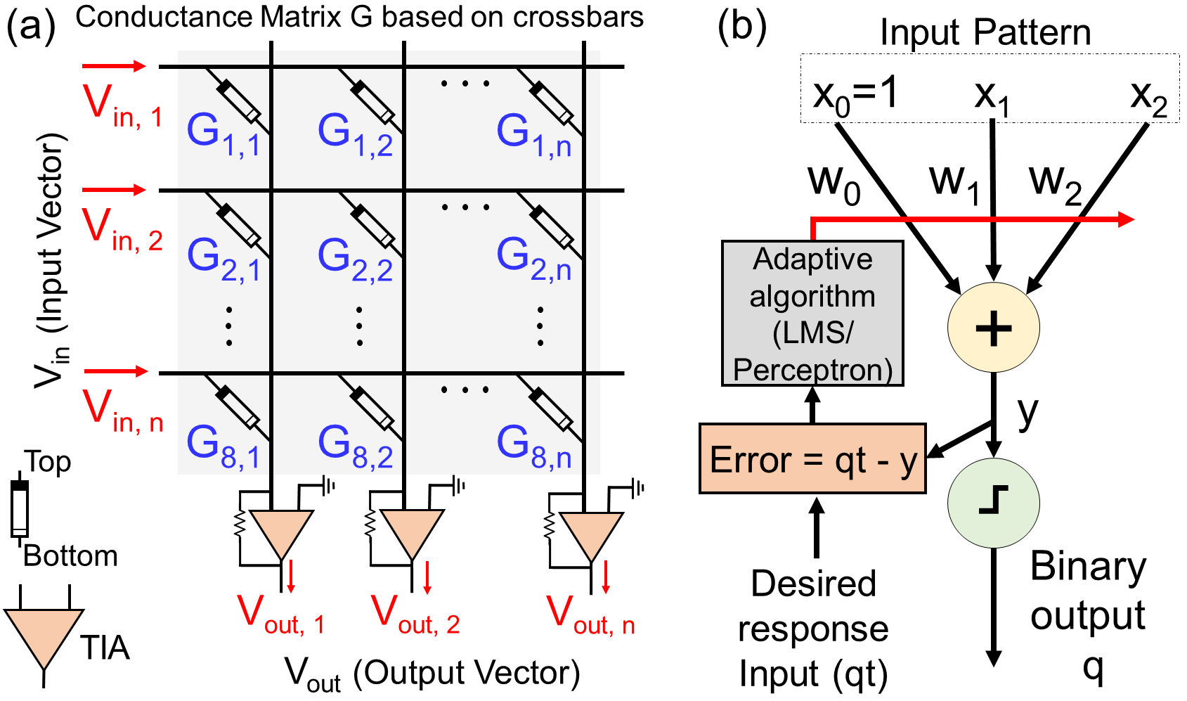
Fig. 1(a) describes the standard implementation of VMM operation in a generic two-terminal resistive nanodevice crossbar based architecture. Input is applied in the form of voltages () across all rows in parallel. Based on the conductance state () of the devices current integrates on each column. The resulting integrated current is converted to voltage using a Trans-Impedance Amplifier (TIA) with feedback resistor (). Output voltage () or the output of VMM operation (across a given column j of the matrix) is defined by Eq. 1:
| (1) |
II-B ADALINE
‘Adaptive Linear Element’ also known as ADALINE, was one of the first networks proposed based on ”memistors” (not memristors) [24]. It is used for a variety of classification applications such as power-quality event detection [25], stereo-vision matching [26], etc. that require fast computation. It is an adaptive threshold logic element representative of a neuron used in ANNs (Artificial Neural Networks). As shown in Fig. 1(b) it consists of an adaptive linear combiner, cascaded with a hard-limiting quantizer, which is used to produce a binary output, = sign (). The bias weight which is connected to a constant input = +1 effectively controls the threshold level of the quantizer. In single-element neural networks, an adaptive algorithm such as Least Mean Square (LMS) or Perceptron rule is used for training weights of ADALINE.
III Proposed Methodology for VMM-based BNN
III-A Training for Binarized-ADALINE
We use a modified version of the training algorithm proposed in [27]. The specific modifications include: (i) Training with only positive value inputs. This helps to simplify input encoding scheme compared to inputs with signed magnitudes as normally used for training BNNs [20]. (ii) Adding support for training a binarized-ADALINE network by using binary ‘tanh’ as the hard-limiting quantizer and binary weights. (iii) Support for training non-vision datasets by use of min-max normalization on input features. The training algorithm is summarized in Algorithm 1. Post-training, binary weights (+1,-1) are generated.
III-B Weight Mapping Strategy
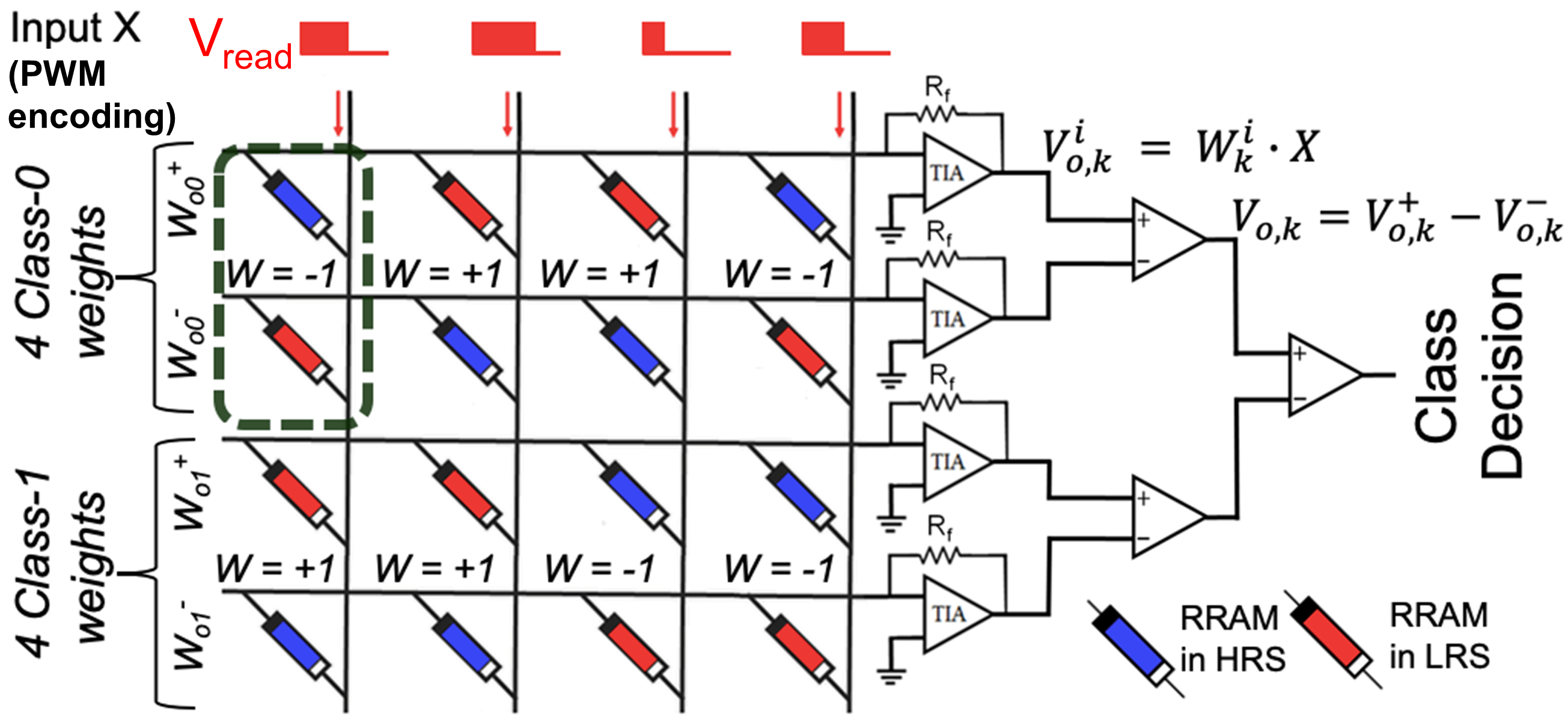
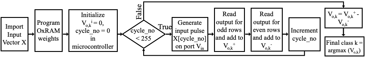
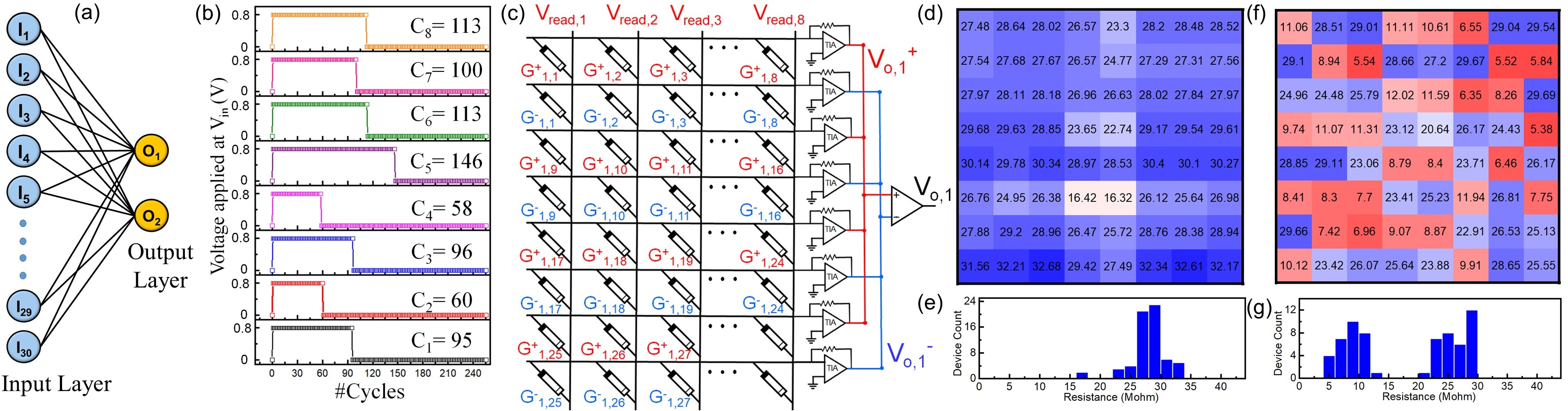
Proposed weight mapping strategy for using two-terminal RRAM device crossbar is shown in Fig. 2. In this discussion, we primarily focus on the binarized-ADALINE as an example network since it represents a basic unit for realization of a multi-layer BNN. Every weight vector is mapped using two separate components i.e. , in consecutive rows of the crossbar. If length of input vector is greater than number of columns, we partition weights and allocate them on separate set of rows. Since two devices are utilized for representing each logical weight (shown in Fig. 2), the utilization of crossbar is reduced by 50%. Summation performed at each row of the crossbar can be represented by Eq. 2 (where denotes output class, denotes polarity i.e. +ve, -ve and denotes partition of feature vector [0,n]). Post summation stage (i.e. TIA output), final sum voltages from rows and are subtracted at the 2nd stage (Eq. 4) leading to a class-wise score , which is used for generating a class decision at the final stage. In case of partitions, all output voltages of a respective polarity (i), for class k () are first stored and summed (Eq. 3) before proceeding to the subtraction and class-decision stages. In proposed binarized-ADALINE, we use analog inputs of 8-bit precision. 8-bit Inputs are realized by utilizing pulse-width modulation (PWM) based encoding which requires integration across 255 cycles to generate the final class score. Fig. 3 summarizes sequence of operations.
| (2) | |||
| (3) | |||
| (4) |
IV Experimental Results
IV-A Testbench & Dataset
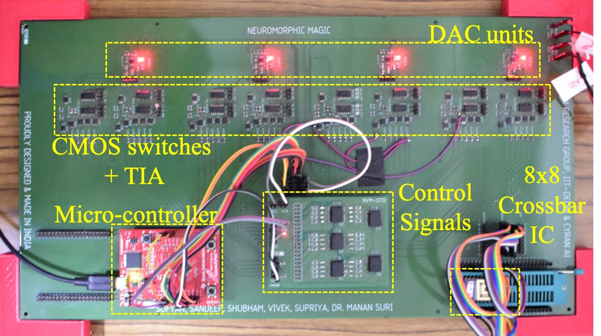
Fig. 4 shows the custom-testbench built for this application. The main components are:
-
1.
: Drives the overall VMM operation scheduling. It is also used for communication with host PC, managing control signals to all other ICs, OxRAM crossbar programming/sensing/ weight-mapping partitioning, computation of outputs post-TIA stage, final class score computation and inference decision.
-
2.
: Consists of TIA for converting current to voltage signal and ADC unit (from micro-controller).
-
3.
: For generating required OxRAM programming signals. We used Vset = 3.3 V, Vreset = -5.5 V and Vread = -0.8 V for programming OxRAM devices in our crossbar. (High values of Vset,Vreset are used in our prototype devices as they have large active area (100 100 ). Negative Vreset,Vread were realized by applying +ve voltage signals at the bottom electrode of OxRAM device and grounding the top electrode, thereby generating effective -ve VTB (where VTB = VTop - VBottom).
-
4.
: For path selection (during SET, RESET and READ operation) and compliance current control.
For validation of the proposed methodology, we trained the binarized-ADALINE network using a binary classification dataset (Breast Cancer dataset) from the UCI machine learning repository [23]. The dataset consists of 357 benign and 212 malignant cells.
IV-B Fabricated OxRAM Crossbar Chip
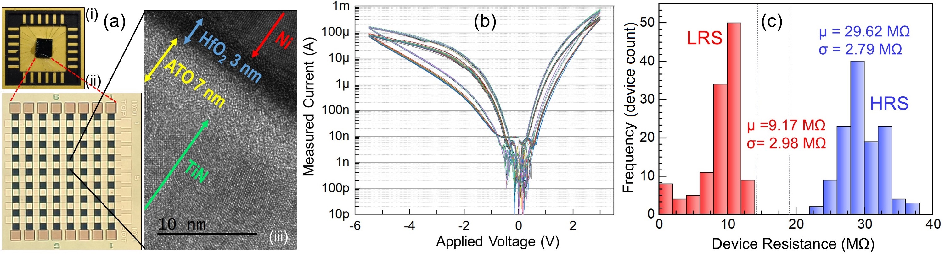
88 OxRAM crossbar with resistive switching stack of Ni/3-nm HfO2/7 nm Al-doped-TiO2/TiN (shown in Fig. 5(a)) was fabricated for this study. First, 500 nm thick TiN film was deposited on thermal-SiO2 (500 nm)/Si wafer by reactive DC sputtering. The wordlines were then patterned by optical photolithography (first mask) and dry etching using inductively-coupled plasma (ICP). The bottom, 7 nm thick ATO dielectric, was then deposited by interchanging varying amount of TiO2 and Al2O3 PE-ALD cycles. Upper, 3 nm thick dielectric HfO2 film, was deposited using TDMAHf (Tetrakis(dimethylamido)hafnium) and O2 plasma. All depositions were carried out at 250 ∘C using remote plasma hot-wall reactor PE-ALD system. The TE pattern (similar to the BE pattern but rotated 90∘) was defined using second mask and 100 nm thick Ni top electrode film was deposited by DC sputtering and patterned using lift-off technique. This way, an 88 crossbar was formed with 100 m wide perpendicular TiN and Ni wordlines and bitlines sandwiching the dielectric bilayer, forming 64 OxRAM devices with 100x100 m2 active area at each crosspoint. The third mask and ICP dry etching step was performed to open the contact windows (etch the dielectrics) to the wordline contact pads. Wire bonding and packaging were the final steps for the OxRAM crossbar encapsulation. DC IV characteristics of 64 OxRAM devices in the 88 crossbar are overlaid in Fig. 5(b). In our study, we have used two distinguishable well separated OxRAM resistance states (HRS/LRS) as shown in Fig. 5(c).
IV-C BNN Results on OxRAM Crossbar
To perform BNN computation with OxRAM crossbar, row-level READ operations were used. Since we used Vread = -0.8 V, due to negative read voltage current integration happened over the row elements. For binarized-ADALINE network (see Fig. 6(a)), we partitioned and mapped the weight vector over multiple rows (shown in Fig. 6(c)) and performed VMM operations. The output class was decided by Eq. 4 as described in Section III-B. The 8-bit wide positive input values were encoded as PWM duty cycles applied to crossbar columns (Fig. 6(b)) leading to current integration over time. In PWM encoding, the input value (ranging from 0 to 255) was translated to pulses with fixed voltage (0.8 V). Specific pulse-widths were n17 ms (where n= number of clock cycles [0-255]). Prior to executing VMM operations the entire crossbar was initialized to HRS (Fig. 6(d,e)) for reliable weight programming. Crossbar resistance distribution post-mapping of trained weights is shown in Fig. 6 (f, g). Training was performed on 80% of the UCI cancer dataset with random shuffling. Classification accuracy results are shown in Table I. We can observe a reduction in classification accuracy between simulated and experimental network. The drop in accuracy can be attributed to sneak-path issue inherent to crossbars. Due to sneak-path leakage, the effective integrated current value across a specific row is diminished. Another factor contributing to accuracy loss is the variability in OxRAM device programming (i.e. LRS and HRS distributions) as evident from Fig. 5(c), 6(g). An effective strategy to mitigate these effects would be to implement two separate ADALINE networks in place of a single neuron. Deep binarized multi-layer networks can also be explored, using larger RRAM arrays to further improve the learning performance as shown in simulation studies [28, 29, 30]. It should be noted that by using binary OxRAM states (HRS/LRS), we have limited the effect of variability that would otherwise reflect in an analog resistance VMM implementation. Furthermore, using OxRAM crossbar solely for inference relaxes the endurance requirements for the devices.
| Sr. No. | Platform | Training Accuracy % | Testing Accuracy % |
|---|---|---|---|
| 1 | Simulation (Software) | 74.06 | 78.07 |
| 2 | Experimental (88 OxRAM Crossbar) | 68.13 | 67.54 |
V Conclusion
In this paper, we presented a novel methodology for mapping BNN operations on two-terminal binary NVM device based crossbars of arbitrary sizes. We experimentally demonstrate the realization of a binarized-ADALINE classifier, for UCI Cancer dataset, on fabricated 88 OxRAM crossbar. The demonstrated methodology can be extended to deeper BNNs through proposed energy-efficient in-memory VMM computation strategy.
Acknowledgement
This work was supported in part by SERB-CRG/2018/001901 and CYRAN AI Solutions.
References
- [1] A. Shafiee, A. Nag, N. Muralimanohar, R. Balasubramonian, J. P. Strachan, M. Hu, R. S. Williams, and V. Srikumar, “ISAAC: A convolutional neural network accelerator with in-situ analog arithmetic in crossbars,” in 2016 ACM/IEEE 43rd Annual International Symposium on Computer Architecture (ISCA). IEEE, jun 2016. [Online]. Available: https://doi.org/10.1109%2Fisca.2016.12
- [2] M. Hu, R. S. Williams, J. P. Strachan, Z. Li, E. M. Grafals, N. Davila, C. Graves, S. Lam, N. Ge, and J. J. Yang, “Dot-product engine for neuromorphic computing,” in Proceedings of the 53rd Annual Design Automation Conference on - DAC16. ACM Press, 2016. [Online]. Available: https://doi.org/10.1145%2F2897937.2898010
- [3] S. N. Truong, K. V. Pham, W. Yang, and K.-S. Min, “Sequential memristor crossbar for neuromorphic pattern recognition,” IEEE Transactions on Nanotechnology, vol. 15, no. 6, pp. 922–930, nov 2016. [Online]. Available: https://doi.org/10.1109%2Ftnano.2016.2611008
- [4] M. A. Lastras-Montano, B. Chakrabarti, D. B. Strukov, and K.-T. Cheng, “3d-DPE: A 3d high-bandwidth dot-product engine for high-performance neuromorphic computing,” in Design, Automation & Test in Europe Conference & Exhibition (DATE), 2017. IEEE, mar 2017. [Online]. Available: https://doi.org/10.23919%2Fdate.2017.7927183
- [5] Y. Jeong and W. Lu, “Neuromorphic computing using memristor crossbar networks: A focus on bio-inspired approaches,” IEEE Nanotechnology Magazine, vol. 12, no. 3, pp. 6–18, sep 2018. [Online]. Available: https://doi.org/10.1109%2Fmnano.2018.2844901
- [6] S.-Y. Sun, H. Xu, J. Li, Q. Li, and H. Liu, “Cascaded architecture for memristor crossbar array based larger-scale neuromorphic computing,” IEEE Access, vol. 7, pp. 61 679–61 688, 2019. [Online]. Available: https://doi.org/10.1109%2Faccess.2019.2915787
- [7] X. Hu, S. Duan, L. Wang, and X. Liao, “Memristive crossbar array with applications in image processing,” Science China Information Sciences, vol. 55, no. 2, pp. 461–472, dec 2011. [Online]. Available: https://doi.org/10.1007%2Fs11432-011-4410-9
- [8] Y. Wang, X. Li, H. Yu, L. Ni, W. Yang, C. Weng, and J. Zhao, “Optimizing boolean embedding matrix for compressive sensing in RRAM crossbar,” in 2015 IEEE/ACM International Symposium on Low Power Electronics and Design (ISLPED). IEEE, jul 2015. [Online]. Available: https://doi.org/10.1109%2Fislped.2015.7273483
- [9] S. Choi, J. H. Shin, J. Lee, P. Sheridan, and W. D. Lu, “Experimental demonstration of feature extraction and dimensionality reduction using memristor networks,” Nano Letters, vol. 17, no. 5, pp. 3113–3118, may 2017. [Online]. Available: https://doi.org/10.1021%2Facs.nanolett.7b00552
- [10] F. Alibart, E. Zamanidoost, and D. B. Strukov, “Pattern classification by memristive crossbar circuits using ex situ and in situ training,” Nature Communications, vol. 4, no. 1, jun 2013. [Online]. Available: https://doi.org/10.1038%2Fncomms3072
- [11] A. Mondal and A. Srivastava, “In-situ stochastic training of MTJ crossbar based neural networks,” in Proceedings of the International Symposium on Low Power Electronics and Design - ISLPED '18. ACM Press, 2018. [Online]. Available: https://doi.org/10.1145%2F3218603.3218616
- [12] L. Wang, W. Gao, L. Yu, J.-Z. Wu, and B.-S. Xiong, “Multiple-matrix vector multiplication with crossbar phase-change memory,” Applied Physics Express, vol. 12, no. 10, p. 105002, sep 2019. [Online]. Available: https://doi.org/10.7567%2F1882-0786%2Fab4002
- [13] M. Jerry, P.-Y. Chen, J. Zhang, P. Sharma, K. Ni, S. Yu, and S. Datta, “Ferroelectric FET analog synapse for acceleration of deep neural network training,” in 2017 IEEE International Electron Devices Meeting (IEDM). IEEE, dec 2017. [Online]. Available: https://doi.org/10.1109%2Fiedm.2017.8268338
- [14] J. Tang, D. Bishop, S. Kim, M. Copel, T. Gokmen, T. Todorov, S. Shin, K.-T. Lee, P. Solomon, K. Chan, W. Haensch, and J. Rozen, “ECRAM as scalable synaptic cell for high-speed, low-power neuromorphic computing,” in 2018 IEEE International Electron Devices Meeting (IEDM). IEEE, dec 2018. [Online]. Available: https://doi.org/10.1109%2Fiedm.2018.8614551
- [15] M. R. Mahmoodi and D. Strukov, “An ultra-low energy internally analog, externally digital vector-matrix multiplier based on NOR flash memory technology,” in 2018 55th ACM/ESDA/IEEE Design Automation Conference (DAC). IEEE, jun 2018. [Online]. Available: https://doi.org/10.1109%2Fdac.2018.8465804
- [16] S. H. Tan, P. Lin, H. Yeon, S. Choi, Y. Park, and J. Kim, “Perspective: Uniform switching of artificial synapses for large-scale neuromorphic arrays,” APL Materials, vol. 6, no. 12, p. 120901, dec 2018. [Online]. Available: https://doi.org/10.1063%2F1.5049137
- [17] H. Tsai, S. Ambrogio, P. Narayanan, R. M. Shelby, and G. W. Burr, “Recent progress in analog memory-based accelerators for deep learning,” Journal of Physics D: Applied Physics, vol. 51, no. 28, p. 283001, jun 2018. [Online]. Available: https://doi.org/10.1088%2F1361-6463%2Faac8a5
- [18] K. Moon, S. Lim, J. Park, C. Sung, S. Oh, J. Woo, J. Lee, and H. Hwang, “RRAM-based synapse devices for neuromorphic systems,” Faraday Discussions, vol. 213, pp. 421–451, 2019. [Online]. Available: https://doi.org/10.1039%2Fc8fd00127h
- [19] Y. Cassuto, S. Kvatinsky, and E. Yaakobi, “Information-theoretic sneak-path mitigation in memristor crossbar arrays,” IEEE Transactions on Information Theory, vol. 62, no. 9, pp. 4801–4813, sep 2016. [Online]. Available: https://doi.org/10.1109%2Ftit.2016.2594798
- [20] M. Courbariaux, I. Hubara, D. Soudry, R. El-Yaniv, and Y. Bengio, “Binarized neural networks: Training deep neural networks with weights and activations constrained to+ 1 or-1,” arXiv preprint arXiv:1602.02830, 2016.
- [21] S. Liang, S. Yin, L. Liu, W. Luk, and S. Wei, “FP-BNN: Binarized neural network on FPGA,” Neurocomputing, vol. 275, pp. 1072–1086, jan 2018. [Online]. Available: https://doi.org/10.1016%2Fj.neucom.2017.09.046
- [22] P. Huang, Z. Zhou, Y. Zhang, Y. Xiang, R. Han, L. Liu, X. Liu, and J. Kang, “Hardware implementation of RRAM based binarized neural networks,” APL Materials, vol. 7, no. 8, p. 081105, aug 2019. [Online]. Available: https://doi.org/10.1063%2F1.5116863
- [23] D. Dua and C. Graff, “UCI machine learning repository,” 2017. [Online]. Available: http://archive.ics.uci.edu/ml
- [24] B. Widrow and M. Lehr, “30 years of adaptive neural networks: perceptron, madaline, and backpropagation,” Proceedings of the IEEE, vol. 78, no. 9, pp. 1415–1442, 1990.
- [25] T. Abdel-Galil, E. El-Saadany, and M. Salama, “Power quality event detection using adaline,” Electric Power Systems Research, vol. 64, no. 2, pp. 137–144, 2003.
- [26] G. Pajares and J. M. de la Cruz, “Local stereovision matching through the ADALINE neural network,” Pattern Recognition Letters, vol. 22, no. 14, pp. 1457–1473, dec 2001. [Online]. Available: https://doi.org/10.1016%2Fs0167-8655%2801%2900097-6
- [27] B. Moons, K. Goetschalckx, N. V. Berckelaer, and M. Verhelst, “Minimum energy quantized neural networks,” in 2017 51st Asilomar Conference on Signals, Systems, and Computers. IEEE, oct 2017. [Online]. Available: https://doi.org/10.1109%2Facssc.2017.8335699
- [28] T. Hirtzlin, B. Penkovsky, J.-O. Klein, N. Locatelli, A. F. Vincent, M. Bocquet, J.-M. Portal, and D. Querlioz, “Implementing binarized neural networks with magnetoresistive ram without error correction,” arXiv preprint arXiv:1908.04085, 2019.
- [29] M. E. Fouda, S. Lee, J. Lee, A. Eltawil, and F. Kurdahi, “Mask technique for fast and efficient training of binary resistive crossbar arrays,” IEEE Transactions on Nanotechnology, vol. 18, pp. 704–716, 2019. [Online]. Available: https://doi.org/10.1109%2Ftnano.2019.2927493
- [30] Y. Kim, W. H. Jeong, S. B. Tran, H. C. Woo, J. Kim, C. S. Hwang, K.-S. Min, and B. J. Choi, “Memristor crossbar array for binarized neural networks,” AIP Advances, vol. 9, no. 4, p. 045131, apr 2019. [Online]. Available: https://doi.org/10.1063%2F1.5092177