Determination of -factor in InAs two-dimensional electron system by capacitance spectroscopy
Abstract
We determine the effective -factor () of a two-dimensional electron gas (2DEG) using a new method based on capacitance spectroscopy. The capacitance-voltage profile of a 2DEG in an InAs/AlGaSb quantum well measured in an in-plane magnetic field shows a double-step feature that indicates the Zeeman splitting of the subband edge. The method allows for simultaneous and independent determination of and effective mass . Data suggest that the biaxial tensile strain in the InAs layer has considerable impacts on both and . Our method provides a means to determine that is complementary to the commonly used coincidence technique.
The electron -factor is a fundamental quantity that governs the coupling between the spin degree of freedom and external magnetic fields. In the solid state, the -factor is altered from its value in vacuum () by spin-orbit coupling and can even change sign, thus becoming a material-dependent parameter referred to as the effective -factor, denoted as . This coupling, making dependent on various parameters such as electric field and quantum confinement, allows for controlling the spin degree of freedom by electrical means, which forms the basis for spintronics and quantum information processing. Wu et al. (2010) Recently, the combination of the strong spin-orbit interaction inherent in narrow-gap semiconductors and external magnetic fields has proven to provide routes to the emergent quantum phase, Alicea (2012); Suominen et al. (2017) where plays an important role. In a two-dimensional electron gas (2DEG), a common platform for various nanostructures and hybrid devices, is determined by a method known as the coincidence technique. Fang and Stiles (1968); Smith III and Fang (1987); Nicholas et al. (1988); Brosig et al. (2000) The method uses magnetic field , with the angle from the sample normal varied to tune the ratio () between the Zeeman splitting and cyclotron energy , where is the Bohr magneton, is Planck’s constant divided by , is the elementary charge, is the perpendicular component of , and is the effective mass. Then is known from at which particular resistance minima disappear due to level coindicence. However, in the presence of , electron-electron interaction can affect in a manner dependent on the Landau-level filling factor. Nicholas et al. (1988); Ando and Uemura (1974) Therefore, alternative means to determine without , which can provide complementary information, will be helpful. In this study, we present a new method based on capacitance spectroscopy that does not require and determine of a 2DEG in a quantum well (QW) of InAs, a narrow-gap semiconductor with strong spin-orbit interaction and large .
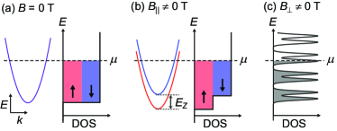
Our method is based on the measurement of quantum capacitance , which is proportional to the thermodynamic density of states (DOS) of the 2DEG Luryi (1988); Ali et al. (2011) [Fig. 1(a)]. Here, is the chemical potential, and is the electron density. We apply a strong in-plane magnetic field and measure the Zeeman splitting of the subband edge [Fig. 1(b)] that appears as a double step in the capacitance-voltage profile. Figure 2(a) shows the equivalent-circuit representation of the system. The differential capacitance (per unit area) between the 2DEG and the front gate, separated by an insulator with dielectric constant and thickness , can be described by a series sum of and geometrical capacitance as
| (1) |
Using this equation along with , where is the front-gate voltage, one can show that the relation
| (2) |
holds between and , Khrapai et al. (2007) where is the threshold voltage at which the 2DEG starts to accumulate. This relation can be used to translate voltage into energy from the measured vs . This allows us to obtain (and hence ) from the double-step feature in the capacitance-voltage profile.
Measurements were conducted at K on a square () device fabricated from a heterostructure grown by molecular beam epitaxy on an -type GaSb (001) substrate. Figure 2(c) depicts the layer structure of the device. The 2DEG is hosted in a 20-nm-wide InAs QW sandwiched by 10-nm-thick Al0.7Ga0.3Sb barriers. The QW structure is flanked on both sides by outer AlAs0.08Sb0.92 barrier layers and capped with -nm GaSb. The AlAs0.08Sb0.92 layers were designed to lattice-match the GaSb substrate and thereby eliminate dislocation formation. Note that the lattice constant of InAs (Al0.7Ga0.3Sb), () Å, is 0.52% smaller (0.53% larger) than that of GaSb ( Å). This induces a biaxial 0.52% tensile (0.53% compressive) strain in the InAs (Al0.7Ga0.3Sb) layer(s). The device has two Ohmic contacts and a front gate with a -nm-thick Al2O3 insulator atomic-layer deposited on the heterostructure. We measured the capacitance between the front gate and the 2DEG 111 Throughout this paper, we use the upper case to denote capacitance to distinguish it from capacitance per area denoted in the lower case. using a capacitance bridge (Andeen-Hagerling 2700A) as a function of [Fig. 2(c)], at a frequency of Hz and an excitation voltage of mVrms. The dissipation factor measured simultaneously with was negligibly small for the range studied, which confirms the irrelevance of charge trapping in the barrier layers. The underlying -GaSb (buffer layer and substrate) was electrically isolated from the 2DEG by the thick AlAs0.08Sb0.92 layer, and therefore did not contribute to . Separate transport measurements on a Hall-bar device fabricated from the same wafer showed that the 2DEG had sheet density of m-2 and low-temperature mobility of m2/Vs at V. Self-consistent envelope-function calculations reveal a slightly asymmetric charge distribution within the QW with negligible penetration into the AlGaSb barriers for the range relevant to the determination [Fig. 2(d)]. A magnetic field of up to T was applied either parallel or perpendicular to the 2DEG.
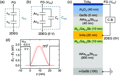
In actual experiments, parasitic capacitance exists, which enters in parallel [Fig. 2(b)]. In addition, is not perfectly constant and varies with as shown below. Therefore, we first show how we determined and by presenting the data obtained at zero magnetic field ( T) and in a perpendicular field . Figure 3(a) shows the measured as a function of . At T, is nearly constant at V, and decreases sharply when the 2DEG is depleted at V. As eq. (1) shows, this sharp decrease represents the contribution of to . In the depletion region ( V), takes a finite value, corresponding to the parasitic capacitance, which mainly stems from the overlap between the front gate and Ohmic electrodes.
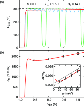
When a perpendicular field is applied, the DOS of the 2DEG splits into a series of peaks due to Landau quantization [Fig. 1(c)]. Accordingly, oscillates as a function of , where the high (low) indicates that the Fermi level lies within a Landau level (between Landau levels). Smith et al. (1985) Notably, maxima of flatten out at a very high field ( T). This happens because, at high fields, the large DOS of Landau levels makes much greater than ; consequently, the second term in eq. (1) becomes negligible. Yu et al. (2013) Hence, we have , where ( mm2) is the area of the 2DEG. 222We estimated by comparing the density obtained by numerically integrating the measured capacitance and that determined from the magneto-capacitance oscillations for – T at various . The % reduction from the lithographic size is likely due to overetching of the mesa side walls. In turn, this implies that, once is known, can be determined experimentally by measuring at a sufficiently strong where . 333 A simple calculation shows that is satisfied for Gaussian Landau-level broadening of meV at T for our sample geometry. In the following analysis, we use the value pF, which we confirmed to be constant at high . 444 This value agrees well with the minimum of at V, which corresponds to the integer quantum Hall effect at Landau-level filling factor 2, where the DOS at the Fermi level is expected to become minimum.
As shown by the dashed line in Fig. 3(a), the values in the flat-top regions can be fitted by a single straight line. The fit line has a finite slope, which indicates that slighty increases with . This is because the 2DEG has a finite width, and its centroid within the QW varies with , reflecting the change in the confinement potential. Hampton et al. (1995); Ali et al. (2011) This effect can be incorporated by representing as
| (3) |
where is measured from the upper interface, is the dielectric constant of the QW, and is a numerical prefactor typically –. Hampton et al. (1995) In the following analysis, we used a linear fit function, like that in Fig. 3(a), to determine as a function of . This allows us to extract from using eq. (1) without the need for knowledge of and . The linear fit agrees with to within pF, with the corresponding errors in and estimated to be less than .
Figure 3(b) plots obtained from the data at T as a function of . The shows a sharp onset at V, where the 2DEG appears, and increases slowly with at a nearly constant slope, except in the vicinity of the onset. To check the validity of our analysis, we calculated from using the relation and compared it with the existing theoretical models Lin-Chung and Yang (1993) for [inset of Fig. 3(b)]. The horizontal axis is the energy measured from the subband edge . The experimental data are plotted vs obtained using eq. (2), with defined as the middle point of the step edge in the vs [see Fig. 5(a)]. The experimentally obtained increases with , with the slope in good agreement with the model accounting for the nonparabolicity of the InAs conduction band (dotted line). The quantitative agreement with theory is significantly improved when the effects of the % in-plane tensile strain in the InAs layer are taken into account (dashed line). Yang et al. (1993); Lin-Chung and Yang (1993) The deviation from the linear dependence near the subband edge suggests electron-electron interaction that becomes important at low densities, which will be discussed later. We emphasize, however, that the determination of using eq. (2) is not affected by the value of obtained in our method, for it holds irrespective of the value.
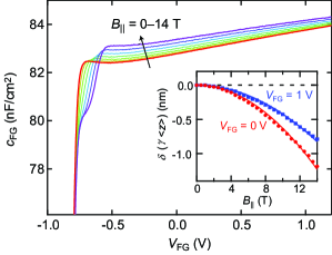
Now we present results obtained with magnetic field applied parallel to the 2DEG. Figure 4 plots vs for – T. The data reveal that at large an extra step feature develops near the onset, indicating the Zeeman splitting of the subband edge, as illustrated in Fig. 1(b). As expected, the step becomes wider as increases. It is worth noting that, aside from the double-step feature, is seen to vary with also in the high- range away from the subband edges. This behavior, not expected from a simple picture, has previously been identified and explained as due to the -induced shift of the wave-function centroid in an asymmetric confinement potential. Stern (1968); Hampton et al. (1995); Jungwirth and Smrčka (1995) To quantify the shift, we translated the change in at each with respect to its value into , which we plot in the inset as a function of for and V. The shift can be fitted well with a quadratic function as . The prefactor is found to be dependent, and can be expressed as nm/T2. Once the centroid shift is absorbed in the dependence of , in the high- region is no longer dependent, as shown in Fig. 5(a), where we plot at and T as a function of . 555 The error in associated with the parabolic approximation of vs (Fig. 4 inset) is negligible compared to that associated with the linear approximation of vs [Fig. 3(a)]. The double steps of at T are nearly equal in height, consistent with the equal DOS for the up and down spin states. If we assume that the Fermi level aligns with the subband bottom at the middle of the step edges [crosses in Fig. 5(a)], we can deduce the energy difference from their separation. Note that the step edges are broadened by disorder, most likely due to background charged impurities, which limits the minimum resolvable to meV in the present experiment.
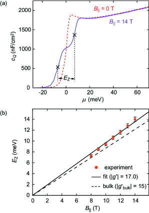
Figure 5(b) plots determined for each . Linear fitting of vs yields . Notably, this value is larger than that of bulk InAs (). Pidgeon et al. (1967); Konopka (1967) In QWs, depends on the well width, reflecting the quantum confinement, which can be understood in terms of the energy dependence of . With the Kane model, Kiselev et al. (1998)
| (4) |
where is the energy measured from the bottom of the bulk conduction band , is the band gap, is the spin-orbit splitting of the valence band, and with the electron mass in vacuum and the Kane momentum-matrix element. With the parameters for InAs ( eV, eV, and eV), Vurgaftman et al. (2001) eq. (4) predicts that varies from at the conduction-band bottom () to, e.g., at eV. The reported value for a -nm-wide InAs/AlSb QW, obtained using the coincidence technique, Brosig et al. (2000) can therefore be explained by eq. (4) if the Fermi level lies eV above the conduction-band bottom of bulk InAs. However, quantum confinement cannot account for greater than the bulk value we observed. We estimate eV in our -nm-wide QW due to quantum confinement ( eV), which would yield . As we argue below, the reduction of due to biaxial tensile strain can override the effects of on . If we take the energy of the light-hole band, which is at the top of the valence band for biaxial tension, Lin-Chung and Yang (1993) we find that the % strain decreases of InAs by eV (parameters are from Ref. Vurgaftman et al., 2001). Applying this value to eq. (4) together with eV, we have . Although a more elaborate theory, as that for in Ref. Lin-Chung and Yang, 1993, is required for a rigorous discussion, our result suggests that the strain effect on is important in heterostructures as well as in nanowires and quantum dots; it can be comparable to or even override the effects of quantum confinement for the case of tensile strain and therefore must be taken into account to discuss subtle effects, such as electron-electron interaction that becomes important at low density. Tsukazaki et al. (2008)
We point out several differences between our method and the coincidence technique. Firstly, the latter provides only the product ; hence, an accurate determination of requires precise knowledge of . This is not the case for our method; as we demonstrated in this study, it allows for simultaneous and independent determination of and . Yet, our method requires large for the double-step feature to be resolved in the capacitance-voltage profile. Secondly, in our method, is determied at a rather low electron density at which the upper-spin subband is depopulated and the system becomes fully spin polarized. The corresponding depends on and . In the present case of InAs, where leads to a rather large of m-2 at T, this value is still much smaller than the typical densities in coincidence experiments. Thirdly, while the coincidence technique assumes to be isotropic, our method selectively measures the in-plane -factor. These differences will allow our method to provide information complementary to coincidence experiments and make it useful in some situations, such as for investigating the effects of electron-electron interaction on and in the absence of perpendicular magnetic fields.
Acknowledgements The authors thank Hiroaki Murofushi for processing the device. This work was supported by JSPS KAKENHI Grant No. JP15H05854.
References
- Wu et al. (2010) M. W. Wu, J. H. Jiang, and M. Q. Weng, Phys. Rep. 493, 61 (2010).
- Alicea (2012) J. Alicea, Reports Prog. Phys. 75, 076501 (2012).
- Suominen et al. (2017) H. J. Suominen, M. Kjaergaard, A. R. Hamilton, J. Shabani, C. J. Palmstrøm, C. M. Marcus, and F. Nichele, Phys. Rev. Lett. 119, 176805 (2017).
- Fang and Stiles (1968) F. F. Fang and P. J. Stiles, Phys. Rev. 174, 823 (1968).
- Smith III and Fang (1987) T. P. Smith III and F. F. Fang, Phys. Rev. B 35, 7729 (1987).
- Nicholas et al. (1988) R. J. Nicholas, R. J. Haug, K. v. Klitzing, and G. Weimann, Phys. Rev. B 37, 1294 (1988).
- Brosig et al. (2000) S. Brosig, K. Ensslin, A. G. Jansen, C. Nguyen, B. Brar, M. Thomas, and H. Kroemer, Phys. Rev. B 61, 13045 (2000).
- Ando and Uemura (1974) T. Ando and Y. Uemura, J. Phys. Soc. Japan 37, 1044 (1974).
- Luryi (1988) S. Luryi, Appl. Phys. Lett. 52, 501 (1988).
- Ali et al. (2011) A. Ali, H. Madan, R. Misra, A. Agrawal, P. Schiffer, J. B. Boos, B. R. Bennett, and S. Datta, IEEE Trans. Electron Devices 58, 1397 (2011).
- Khrapai et al. (2007) V. S. Khrapai, A. A. Shashkin, M. G. Trokina, V. T. Dolgopolov, V. Pellegrini, F. Beltram, G. Biasiol, and L. Sorba, Phys. Rev. Lett. 99, 086802 (2007).
- Note (1) Throughout this paper, we use the upper case to denote capacitance to distinguish it from capacitance per area denoted in the lower case.
- Lin-Chung and Yang (1993) P. J. Lin-Chung and M. J. Yang, Phys. Rev. B 48, 5338 (1993).
- Smith et al. (1985) T. P. Smith, B. B. Goldberg, P. J. Stiles, and M. Heiblum, Phys. Rev. B 32, 2696 (1985).
- Yu et al. (2013) G. L. Yu, R. Jalil, B. Belle, A. S. Mayorov, P. Blake, F. Schedin, S. V. Morozov, L. A. Ponomarenko, F. Chiappini, S. Wiedmann, U. Zeitler, M. I. Katsnelson, A. K. Geim, K. S. Novoselov, and D. C. Elias, Proc. Natl. Acad. Sci. U. S. A. 110, 3282 (2013).
- Note (2) We estimated by comparing the density obtained by numerically integrating the measured capacitance and that determined from the magneto-capacitance oscillations for – T at various . The % reduction from the lithographic size is likely due to overetching of the mesa side walls.
- Note (3) A simple calculation shows that is satisfied for Gaussian Landau-level broadening of meV at T for our sample geometry.
- Note (4) This value agrees well with the minimum of at V, which corresponds to the integer quantum Hall effect at Landau-level filling factor 2, where the DOS at the Fermi level is expected to become minimum.
- Hampton et al. (1995) J. Hampton, J. Eisenstein, L. Pfeiffer, and K. West, Solid State Commun. 94, 559 (1995).
- Yang et al. (1993) M. J. Yang, P. J. Lin-Chung, B. V. Shanabrook, J. R. Waterman, R. J. Wagner, and W. J. Moore, Phys. Rev. B 47, 1691 (1993).
- Stern (1968) F. Stern, Phys. Rev. Lett. 21, 1687 (1968).
- Jungwirth and Smrčka (1995) T. Jungwirth and L. Smrčka, Phys. Rev. B 51, 10181 (1995).
- Note (5) The error in associated with the parabolic approximation of vs (Fig. 4 inset) is negligible compared to that associated with the linear approximation of vs [Fig. 3(a)].
- Pidgeon et al. (1967) C. R. Pidgeon, D. L. Mitchell, and R. N. Brown, Phys. Rev. 154, 737 (1967).
- Konopka (1967) J. Konopka, Phys. Lett. A 26, 29 (1967).
- Kiselev et al. (1998) A. A. Kiselev, E. L. Ivchenko, and U. Rössler, Phys. Rev. B 58, 16353 (1998).
- Vurgaftman et al. (2001) I. Vurgaftman, J. R. Meyer, and L. R. Ram-Mohan, J. Appl. Phys. 89, 5815 (2001).
- Tsukazaki et al. (2008) A. Tsukazaki, A. Ohtomo, M. Kawasaki, S. Akasaka, H. Yuji, K. Tamura, K. Nakahara, T. Tanabe, A. Kamisawa, T. Gokmen, J. Shabani, and M. Shayegan, Phys. Rev. B 78, 233308 (2008).