Interplay between Yu-Shiba-Rusinov states and multiple Andreev reflections
Abstract
Motivated by recent scanning tunneling microscopy experiments on single magnetic impurities on superconducting surfaces, we present here a comprehensive theoretical study of the interplay between Yu-Shiba-Rusinov bound states and (multiple) Andreev reflections. Our theory is based on a combination of an Anderson model with broken spin degeneracy and nonequilibrium Green’s function techniques that allows us to describe the electronic transport through a magnetic impurity coupled to superconducting leads for arbitrary junction transparency. Using this combination we are able to elucidate the different tunneling processes that give a significant contribution to the subgap transport. In particular, we predict the occurrence of a large variety of Andreev reflections mediated by Yu-Shiba-Rusinov bound states that clearly differ from the standard Andreev processes in non-magnetic systems. Moreover, we provide concrete guidelines on how to experimentally identify the subgap features originating from these tunneling events. Overall, our work provides new insight into the role of the spin degree of freedom in Andreev transport physics.
I Introduction
The competition between magnetism and superconductivity is one of the most fundamental problems in condensed matter physics. The ability of the scanning tunneling microscope (STM) to manipulate individual magnetic atoms and molecules has enabled to study this competition at the atomic scale. One of the most interesting manifestations of the interplay between these two antagonistic phases of matter is the appearance of the so-called Yu-Shiba-Rusinov (YSR) bound states in the spectrum of a single magnetic impurity coupled to a superconductor or embedded in a superconducting matrix Yu1965 ; Shiba1968 ; Rusinov1969 . Numerous STM-based experiments on single magnetic impurities on surfaces of conventional superconductors have reported the observation of these superconducting bound states Yazdani1997 ; Ji2008 ; Franke2011 ; Menard2015 ; Ruby2015 ; Hatter2015 ; Ruby2016 ; Randeria2016 ; Choi2017 ; Cornils2017 ; Hatter2017 ; Farinacci2018 ; Brand2018 ; Malavolti2018 ; Kezilebieke2019 ; Senkpiel2019 ; Etzkorn2018 ; Schneider2019 ; Liebhaber2020 ; Huang2019a ; Huang2019b , for a recent review see Ref. Heinrich2018 . Those experiments have elucidated many basic aspects of the YSR states such as, for instance, the nature of the many-body ground state Franke2011 ; Hatter2015 ; Hatter2017 , the spatial extension of the YSR wave functions Menard2015 ; Ruby2016 ; Choi2017 , the spin signature Cornils2017 , or the role of key energy scales like the exchange energy Farinacci2018 or the impurity-substrate coupling Huang2019a . Moreover, part of the interest in the YSR states lies in the fact that they can serve as building blocks to create Majorana states in designer structures such as chains of magnetic impurities Nadj-Perge2014 ; Ruby2015b ; Kezilebieke2018 ; Ruby2017 ; Ruby2018 .
Often the STM experiments probing single magnetic impurities on superconducting substrates are done using a superconducting tip to enhance the energy resolution. More importantly for this work, the use of superconducting tips enables to study a variety of tunneling processes, most notably multiple Andreev reflections (MARs), whose relative importance depends on the junction transmission. Let us remind that in a junction between a normal metal and a superconductor, an Andreev reflection consists in a tunneling process in which an electron coming from the normal metal is reflected as a hole of opposite spin transferring a Cooper pair into the superconductor. In the absence of in-gap bound states, this process dominates the subgap transport. In the case of a junction with two superconducting electrodes, one can additionally have MARs in which quasiparticles undergo a cascade of Andreev reflections that give rise to a very complex subgap structure in the current-voltage characteristics. The microscopic theory of MARs, which was developed in the mid-1990s Averin1995 ; Cuevas1996 , was actually quantitatively confirmed in the context of superconducting atomic-size contacts with the help of break-junction techniques and the STM Scheer1997 ; Scheer1998 . In recent years, several STM-based experiments in the context of magnetic impurities on superconducting surfaces have revealed signatures of the interplay between YSR bound states and Andreev reflections Ruby2015 ; Randeria2016 ; Farinacci2018 ; Brand2018 , which demonstrates that this type of system is ideal to study the role of the spin degree of freedom in these tunneling events.
Some of the aspects of the interplay between YSR states and Andreev reflections have already been studied theoretically. For instance, in Ref. Andersen2011 , and motivated by experiments in the context of quantum dots, a theoretical study of the nonlinear cotunneling current through a spinful quantum dot contacted by two superconducting leads was presented. This study concluded that while the subgap transport is dominated by MARs in the limit of symmetric couplings to the superconductors, it is determined by the quasiparticle tunneling into spin-induced YSR states in the strongly asymmetric case (of relevance for our work). On the other hand, Ruby et al. Ruby2015 analyzed in the case of a superconducting tip, both theoretically and experimentally, the competition between the tunneling of single quasiparticles and a resonant Andreev reflection as a function of the junction transmission. In Ref. Brand2018 , the crossover between the tunnel regime (low junction transparency) and the contact regime (high transparency) was theoretically analyzed in connection with the experiments reported in that work with a normal tip. In spite of these interesting works, there is still no systematic theory studying the interplay between YSR states and (multiple) Andreev reflections which identifies all the relevant tunneling events that can occur in these impurity systems and that could serve as a guide for the experimentalists to look for novels features in the subgap transport. The goal of this work is to fill this theoretical gap. For this purpose, we present here a theory of the interplay between YSR states and MARs in junctions where single magnetic impurities are coupled to superconducting leads, with special emphasis on STM-based experiments. Our theory is based on a combination of a mean-field Anderson model with broken spin degeneracy to describe magnetic impurities and nonequilibrium Green’s function techniques to compute the electronic transport properties. Using this combination we elucidate the complete set of relevant tunneling processes that can occur in these systems and provide precise guidelines to experimentally identify the signatures of those processes.
The rest of the manuscript is organized as follows. In section II we describe the system under study and present the theoretical tools that we use to compute the electronic transport properties of magnetic impurities coupled to superconducting leads. In section III we discuss the results for the case where only one of the leads is superconducting to study in detail the competition between single-quasiparticle tunneling and the simplest Andreev reflection. Then, in section IV we present a detailed study of the subgap transport in the case of a magnetic impurity coupled to a superconducting substrate and a superconducting tip, which is the central goal of this work. Finally, in section V we discuss the new lines of research that this work opens and we summarize our main conclusions.
II Systems under study and theoretical approach
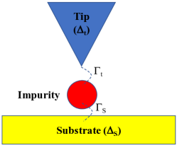
Our goal in this work is to compute the current-voltage characteristics in a system in which a magnetic impurity is coupled to superconducting leads with special emphasis in the interplay between YSR bound states and MARs. As shown schematically in Fig. 1, we shall focus on the analysis of the experimentally relevant situation in which a magnetic impurity (an atom or a molecule) is coupled to a superconducting substrate (S) and to an STM tip (t), which can also be superconducting. This section is devoted to the description of the theoretical tools used to tackle this problem.
II.1 The Anderson model
The Anderson model used here to describe the impurity coupled to superconducting leads is summarized in the Hamiltonian
| (1) |
Here, , with , is the BCS Hamiltonian of the lead given by
| (2) |
where and are the creation and annihilation operators, respectively, of an electron of momentum , energy , and spin in lead , is the superconducting gap, and is the corresponding superconducting phase. On the other hand, is the Hamiltonian of the magnetic impurity, which in our case is given by
| (3) |
where is the occupation number operator on the impurity, is the on-site energy (not to confuse with the Coulomb energy), and is the exchange energy that breaks the spin degeneracy on the impurity. Finally, describes the coupling between the magnetic impurity and the leads that adopts the form
| (4) |
where describes the tunneling coupling between the impurity and the lead and it is chosen to be real.
The Anderson model used here has origin in a mean-field approximation and it provides a convenient way to describe a quantum magnetic impurity note1 . In particular, it has been successfully employed in the past to describe the observation of Andreev bound states in quantum dots coupled to superconducting leads, see e.g. Pillet2010 , and it has been shown to reproduce many of the salient features of the superconducting bound states predicted by more sophisticated many-body approaches Martin-Rodero2011 ; Martin-Rodero2012 . Moreover, it has been shown very recently that this model provides a convenient starting point to illustrate the fundamental role played in the YSR states by the hybridization of the impurity with the substrate Huang2019a . Finally, the Anderson model (beyond the mean-field approximation) is ideally suited for studying the role of electronic correlations in this problem, see e.g. Refs. Martin-Rodero2011 ; Martin-Rodero2012 ; Zitko2015 ; Kadlecova2017 ; Zitko2018 ; Kadlecova2019 and references therein.
For what follows, it is convenient to rewrite the previous Hamiltonian in terms of four-dimensional spinors that live in a space resulting from the direct product of the spin space and the Nambu (electron-hole) space. In the case of the leads, the relevant spinor is defined as
| (5) |
while for the impurity states we define
| (6) |
Using the notation and () for Pauli matrices in Nambu and spin space, respectively, and with and as the unit matrices in those spaces, it is straightforward to show that the Hamiltonian in Eq. (1) can be cast into the form
| (7a) | |||||
| (7b) | |||||
| (7c) | |||||
where
| (8a) | |||||
| (8b) | |||||
| (8c) | |||||
II.2 Bare Green’s functions
The starting point for the calculation of the electronic transport properties will be the bare Green’s functions of the different subsystems which can be easily calculated from the previous matrix Hamiltonians as follows. First, the retarded and advanced Green’s functions of the leads resolved in -space are defined as , where and is a positive infinitesimal parameter, which we shall drop out to simplify things along with the superscript , unless they are strictly necessary. Summing over , , where is the normal density of states at the Fermi energy of lead , we arrive at the standard expression for the bulk Green’s function of a BCS superconductor
| (9) |
On the other hand, the impurity Green’s function is given by
| (14) | |||||
Given that in an experimental setup the coupling of the impurity to the STM tip is weaker than the coupling to the substrate, a natural division of the system, which will be very useful in the transport calculations, is to consider the tip on one side and the impurity-substrate system on the other side. The dressed Green’s function of the impurity taking into account the coupling to the superconducting substrate is calculated by solving the Dyson equation
| (15) |
where the indices run over and , the bare Green’s functions and are given by Eqs. (14) and (9), respectively, and the couplings are given by . This Dyson equation can be easily solved to obtain
| (16) |
with
| (17) |
where
| (18) | |||||
Here, and and we have defined the tunneling rate (a similar rate describes the strength of the tip-impurity coupling).
II.3 Computing the current-voltage characteristics
To compute the electronic transport properties in our model system, we shall assume that the voltage drops at the interface between the impurity and the STM tip, which is justified by the fact that usually the tip-impurity coupling is clearly weaker than the substrate-impurity coupling. As mentioned above, with this assumption the natural division of the system to apply the standard nonequilibrium techniques is such that the left subsystem is the STM tip and the right system is the combination of the magnetic impurity and the superconducting substrate. With this division, we can treat our system as a single-channel point contact in which the effective Hamiltonian reads Cuevas1996
| (19) |
where is now the BCS Hamiltonian of the tip, is the Hamiltonian of the impurity coupled to the substrate, is the tunneling rate describing the coupling between the impurity and the tip, and is the time-dependent superconducting phase difference, with being the applied voltage and is the dc part of this phase difference. In the coupling term of this Hamiltonian L and R stand for the outermost sites of each electrode and, in particular, R corresponds now to the dressed impurity site. With this starting point, the calculation of the current-voltage characteristics can be done following the theory of MARs described in Ref. Cuevas1996 , where things need to be slightly modified to accommodate for the breaking of the spin degeneracy in this case, as we describe in what follows.
First, we evaluate the current at the interface between the two electrodes (L and R), which adopts the form
| (20) | |||||
The nonequilibrium expectation values appearing in the previous equation can be written in terms of the lesser Green’s functions which in the spin-Nambu representation are given by
| (21) |
Here, is the time-ordering operator on the Keldysh contour such that any time in the lower branch () is larger than any time in the upper one (). Moreover, and the four-component spinors and are defined following the conventions of Eqs. (5) and (6). Thus, the current can now be written as
| (22) | |||||
where Tr is the trace taken over Nambu and spin degrees of freedom and are the coupling matrices in spin-Nambu space.
To determine the dressed Green’s functions appearing in the current formula we follow a perturbative scheme and treat the coupling term in the Hamiltonian of Eq. (19) as a perturbation. The unperturbed Green’s functions, , correspond to the uncoupled electrodes in equilibrium. To be precise, the bare Green’s function is given by Eq. (9) and the bare Green’s function of the impurity coupled to the substrate is given by Eq. (16) [without the superconducting phase that has been moved to the couplings]. On the other hand, it is convenient to express the current by means of the so-called T-matrix. The T-matrix associated to the time-dependent perturbation in Eq. (19) is defined as
| (23) |
where the product is a shorthand for convolution, i.e., for integration over intermediate time arguments. As shown in Ref. Cuevas1996 , the exact current including all the orders in the tunneling rate can be written in terms of the T-matrix components as
| (24) | |||||
In order to solve the T-matrix integral equations it is convenient to Fourier transform with respect to the temporal arguments
| (25) |
Because of the time dependence of the coupling matrices, one can show that admits the following general solution
| (26) |
Thus, one can show that the current has the time dependence
| (27) |
where the current amplitudes can be expressed in terms of the T-matrix Fourier components, , as
| (28) | |||||
where we have used the notation , notice that the bare Green’s functions are diagonal in energy space, and the bare lesser Green’s functions are given by , where is the Fermi function with being the temperature. The previous formula can be further simplified by using the general relation , which reduces the calculation of the current to the determination of the Fourier components fulfilling the following set of linear algebraic equations
| (29) | |||||
where the different matrix coefficients are given in terms of the unperturbed Green’s functions as follows
| (30) |
In general, these block-tridiagonal systems have to be solved numerically and the current can only be expressed in an analytical form in a few limiting cases, as we discuss below. On the other hand, let us stress that we shall focus here exclusively on the discussion of the dc current, i.e., in Eq. (27), and we shall not analyze the (zero-bias) dc Josephson current. To conclude this discussion let us say that the formalism presented here is not strictly necessary in the case of a single impurity with spin-preserving tunneling, and the transport properties of our model system can be equivalently described within a formalism (using only the Nambu space). However, the approach provides a convenient platform that illustrates the key role of the spin and it becomes absolutely necessary in more complex situations like, for instance, those involving the tunneling between magnetic impurities with noncollinear spins Huang2019b .
II.4 YSR states and tunneling spectra
Obviously, the transport properties will reflect the electronic structure of the magnetic impurity. In particular, due to the coupling of the impurity with the superconducting substrate, this electronic structure will exhibit both Andreev and YSR bound states in the gap region. In the limit in which we can ignore the coupling to the STM tip (), the local density of states (LDOS) projected onto the impurity site is given by
| (31) |
where
| (32) |
where and is given by Eq. (18). Here, is a phenomenological parameter that describes the inelastic broadening of the electronic states. The condition for the appearance of superconducting bound states is . In particular, the spin-induced YSR states appear in the limit (and they are inside the gap when also ). In this case, there is a pair of fully spin-polarized YSR bound states at energies (measured with respect to the Fermi energy) Huang2019a
| (33) |
which has a similar structure as in the case of the classical Shiba model Salkola1997 ; Flatte1997a ; Flatte1997b ; Balatsky2006 . This is more apparent in the electron-hole symmetric case , where the previous expression reduces to
| (34) |
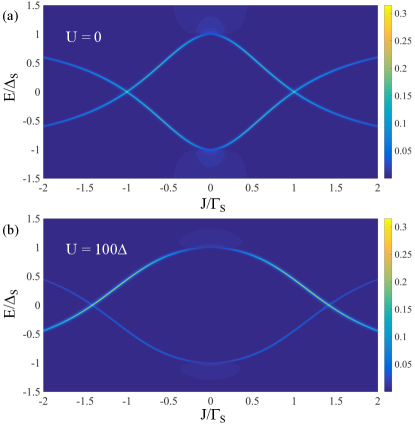
For future reference, we present in Fig. 2 two representative cases of the LDOS in the impurity when it is only coupled to the substrate for a case with electron-hole symmetry (upper panel) and a case in which this symmetry is broken (lower panel). Notice the appearance of a pair of YSR states inside the gap whose dependence on the exchange energy is accurately described by the analytical formula of Eq. (33). Notice also that the two states cross at zero energy when , which is the point that corresponds to the quantum critical point Balatsky2006 . Finally, it is also worth noticing the absence of singularities at , which is a simple consequence of the appearance of the YSR states and the conservation of the number of states.
As a next step, we briefly remind how the presence of the YSR states is reflected in the tunneling spectra acquired with a superconducting tip, i.e., when the tip is sufficiently far away such that and the only relevant tunneling process is the single-quasiparticle tunneling. In this case, one use the approximation in Eq. (29) to arrive at the following analytical expression
| (35) |
where is the Fermi function, is the dimensionless BCS DOS of the tip, and is total (including both spin contributions) LDOS in the impurity given by Eqs. (31) and (32). In Fig. 3 we illustrate the lineshapes of the differential conductance (in units of the quantum of conductance ) in the tunnel regime for different values of the exchange energy in the impurity and for two different values of impurity on-site energy: and . Here, we assume that the gaps of the tip and substrate are equal: . Notice that in all cases the most prominent feature is the appearance of a conductance peak at , which is accompanied by a negative differential conductance (except in the case where there are no YSR states and one recovers the standard coherent peaks at ). Notice also that the differential conductance is symmetric, i.e., independent of the bias polarity, when there is electron-hole symmetry, see panel (a), and asymmetric when the electron-hole symmetry is broken, see panel (b). It is also worth remarking the absence of coherent peaks at when there is no spin degeneracy, i.e., , which is due to the absence of singularities at the gap edges in the impurity LDOS.
II.5 Normal state conductance
In what follows, and in order to make contact with the experiment, it is important to characterize our system with the normal state conductance, . In the case in which neither the tip nor the substrate are superconducting, the current formula within our model can be worked out analytically and it is given by the following Landauer-type of expression
| (36) |
where the spin-dependent transmission coefficients are given by
| (37) |
Thus, the zero-temperature normal state linear conductance is given by
| (38) |
which in the tunnel regime () reduces to
| (39) |
showing that it is linear in . Moreover, in this work, will always be much smaller than such that the differential conductance in the normal state will be independent of the bias.
III A normal tip: Andreev reflection mediated by YSR states
Since our central goal is the study of the interplay between YSR states and Andreev reflections, it is convenient to first discuss the results for the current-voltage characteristics in the case in which the STM tip is not superconducting. In this case, the total current is the sum of two contributions: the current due to single-quasiparticle tunneling and the current due to an Andreev reflection, which can be mediated by the YSR states, as we shall show below. Assuming that the STM tip is in the normal state, the expression of the current can be worked out analytically for arbitrary range of parameters and it adopts the form
| (40) |
where is the quasiparticle current and the Andreev current. While the expression of the quasiparticle current is too cumbersome and we shall not present it here explicitly, the Andreev current adopts a compact and intuitive form given by
| (41) |
where the Andreev reflection probability is given by
| (42) |
with
| (43) |
Notice that in the limit of weak coupling to the STM tip, , see Eq. (18), where are the denominators whose zeros give us the energies of the YSR states in the case in which the impurity is not coupled to the STM tip.
From the expression above for , one can deduce several important facts. First, since the Andreev reflection probability is always electron-hole symmetric, i.e., , the corresponding contribution of this process to the differential conductance does not depend on the bias polarity: (notice that at low temperatures . This fact was first recognized in Ref. Martin2014 . This is at variance with the single-quasiparticle contribution, which does depend on the bias polarity if the electron-hole symmetry is broken (). On the other hand, the Andreev reflection probability is resonantly enhanced at the energy of the YSR states and therefore, it gives rise to differential conductance peaks at . This is similar to the feature expected from the quasiparticle current, whose corresponding differential conductance increases significantly when the chemical potential of the tip is aligned with the YSR states, i.e., also when . The way to differentiate between the contributions of quasiparticle tunneling and Andreev reflection is by studying how the differential conductance scales with the normal state conductance and by examining the dependence on the bias polarity.
We illustrate the expected results in the case of a normal conducting tip in Fig. 4(a) where we show the differential conductance in a logarithmic scale as a function of the bias voltage and exchange energy for a case with a moderate tunneling rate and electron-hole symmetry (), see figure caption for the value of the other model parameters. In this case the differential conductance is symmetric, , and for this reason we only show the region of positive bias. As expected, the most prominent feature is the appearance of a conductance peak inside the gap () at a bias equal to the energy of the YSR state, which in this case is given by Eq (34).
While the dependence of the differential conductance on the exchange energy is very revealing, it is not easy to investigate experimentally in a continuous manner. In the experiments, it is much easier to control the normal state conductance, which can be done by simply changing the tip-impurity distance. For this reason, we present in Fig. 4(b) an example of the evolution of the differential conductance as a function of the normal state conductance, which we vary here by changing accordingly the tunneling rate . In this case, we have chosen and , which makes the differential conductance independent of the bias polarity. Again, the most salient feature is the appearance of a peak inside the gap at a bias . As the normal state conductance increases, the peak first broadens and then at high transmissions () it becomes a very broad peak at zero bias (not shown here), in agreement with the experimental observations in Ref. Brand2018 and the theoretical discussion presented in that work.
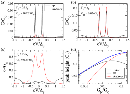
At this stage, the most relevant question concerns the relative contributions to the conductance peak inside the gap of quasiparticle tunneling and Andreev reflection. To answer this question we present in Fig. 5(a-c) these two individual contributions to the differential conductance for three representative values of (or ) corresponding to the results of Fig. 4(b). As one can see, when the normal state conductance (or normal transmission) is sufficiently small, the subgap differential conductance is dominated by the contribution of single-quasiparticle tunneling, as expected. However, as the normal state transmission increases, the Andreev contribution becomes more relevant and eventually, it dominates the subgap conductance and, in particular, the conductance peak at the energy of the YSR state. In this particular example both contributions become of the same order when . To illustrate the competition between quasiparticle tunneling and Andreev reflection, we show in Fig. 5(d) the contribution of these two processes to the conductance peak as a function of the normal state conductance. As expected, at very low transmissions the peak height scales linearly with , which corresponds to the regime in which single-quasiparticle tunneling dominates the subgap transport. In this regime, the Andreev contribution scales as . Then, there is a crossover to a sublinear regime, which occurs when both contributions to the peak height are of the same order. Finally, for , the peak height is mainly determined by the Andreev reflection. The sublinear behavior in this “high-transmission” regime is a manifestation of the resonant character of the Andreev reflection, or in other words, of the fact that the Andreev reflection is mediated by the presence of a sharp bound state. Notice also that in this regime the single-quasiparticle contribution decreases upon increasing the transmission.
IV A superconducting tip: YSR states and multiple Andreev reflections
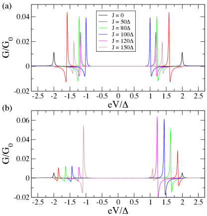
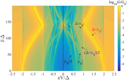
In this section we shall discuss the current-voltage characteristics in the case in which the tip is also superconducting, which is the central goal of this work. For simplicity, we shall assume that the tip and the substrate have the same gap that we shall denote as . In Fig. 6(a) we illustrate the rich subgap structure that appears in the differential conductance as the transmission of the junction increases in a case in which and . The different curves correspond to different values of the tunneling rate , while the coupling to the substrate is kept constant and equal to (this value will be used throughout the whole section). We see new peaks appearing in the differential conductance as the transmission increases, apart from the peaks at that already appear in the deep tunnel regime due to the contribution of single-quasiparticle tunneling. Obviously, those additional features must originate from the contribution of various kinds of Andreev reflections, as we shall clarify below. To support our interpretation, we have added several vertical dashed lines at specific energies/voltages to the graph.
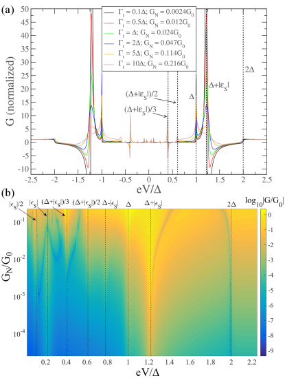
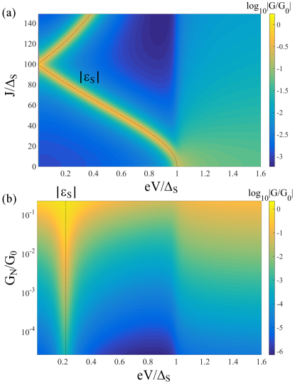
To get further insight into the origin of the subgap structure, we present in Fig. 6(b) a more systematic study of the evolution of the differential conductance as a function of the normal state conductance for the same case as in Fig. 6(a). Notice that for convenience we are plotting here the absolute value of the conductance in logarithmic scale and we focus on positive voltages due to the electron-hole symmetry in this example. We see that in the deep tunnel regime (for ), the conductance spectra are dominated by the presence of a peak at . This is the hallmark expected from the tunneling of single quasiparticles, as we discussed in section II.4, and it has been reported in numerous experimental studies Heinrich2018 . There is also a feature at due to quasiparticle tunneling connecting the gap edges of both electrodes, but it is much less pronounced due to the absence of the BCS singularities in the LDOS of the magnetic impurity. It is worth mentioning that most experimental studies report a pronounced conductance peak at the sum of the gap energies of the tip and the substrate, something that cannot be explained with a model like ours in which there is a single current pathway through the impurity. It has been suggested that these pronounced coherent peaks can be explained by the presence of a second, non-magnetic channel that involves another orbital/level in the impurity Huang2019a . Notably, there are two additional peaks visible in this regime at and , although their heights are orders of magnitude smaller than the one at . One might be tempted to attribute these peaks to different kinds of Andreev reflections, but in fact those features can be accurately reproduced with the tunneling approximation of section II.4 and, therefore, they must originate from single-quasiparticle tunneling. The peak at can be explained by the existence of a small but finite DOS inside the gap in the STM tip due to a finite value of the broadening parameter ( in this example). This peak simply occurs when the chemical potential of the tip is aligned with the empty YSR state and we have checked that its height scales linearly with the normal state conductance . This conductance peak was reported in Ref. Randeria2016 and it was correctly interpreted as a consequence of an “imperfect” tip. On the other hand, the peak at is due to the finite DOS inside the gap region in the impurity (induced by the substrate) due to the finite value of ( in this example) and it appears when the gap edge of the tip is aligned to the chemical potential of the impurity-substrate system. This conductance peak has also been observed experimentally, e.g. in Ref. Randeria2016 . More important for the discussion in this work is the fact that when the junction transmission (or normal state conductance) increases, one observes the appearance of a whole zoo of conductance peaks, whose energies are identified in Fig. 6(b) with the help of vertical dashed lines. The main goal of the rest of this section is to understand the physical origin of those features.
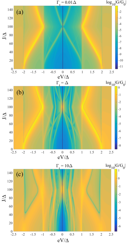
An important hint on the origin of the different peaks in the subgap conductance can be obtained by analyzing how they shift when the energy of the YSR states is modified, for instance, by changing the exchange energy. This is what we illustrate in Fig. 7 where we show the evolution of the differential conductance with the exchange energy for three different values of the tunnel rate and . The case of in panel (a) corresponds to the tunnel regime and these results can be reproduced with the tunneling approximation of section II.4 (not shown here). As expected, we see that the conductance spectra are largely dominated by the appearance of two peaks that disperse with the energy of the YSR states as . Other features that are also visible, albeit much less prominent, appear at , , and . As we explained in the previous paragraph, all of these features can be explained in terms of single-quasiparticle tunneling. For a higher value of the normal state conductance, like in panel (b), there appears a large variety of conductance peaks that cannot be explained by the tunneling of individual quasiparticles. Finally, when the normal state conductance is above , different conductance peaks start to overlap and the subgap structure becomes very complex, as we illustrate in Fig. 7(c) for .
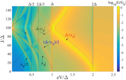
To elucidate the relevant tunneling processes giving rise to the different features of the subgap structure, it is important to identify the exact energies at which these features appear. This is done in detail in Fig. 8 for the case of , panel (b) in Fig. 7, where we focus on positive voltages. We see that there are three different types of energies describing the position of those features. First, there are energies, like with , that only involve the gap energy. Second, there are energies that are a combination of the gap energy and the energy of the YSR bound states like, e.g., or . Finally, there are energies like and that only involve the energy of the YSR states. With this identification we are now ready to propose the whole family of tunneling events that can take place in our system.
In Fig. 9 we summarize the relevant processes that give rise to the different features in the subgap conductance in our system, which we group into four distinct families. The first family, illustrated in Fig. 9(a), is formed by single-quasiparticle tunneling events in which a single electron/hole is transferred through junction. Within these processes, we can differentiate between tunneling events in which a quasiparticle can tunnel from the continuum of an electrode to the continuum of the other electrode, see left scheme in Fig. 9(a), and events that start (end) in the continuum of states of tip and end (start) in the empty YSR state in the impurity, see right scheme in Fig. 9(a). The first type is obviously responsible for the conductance feature at , while the second one gives rise to the conductance peaks at . As discussed above, if there is some residual DOS inside the gap region in the electrodes, one can have additional single-quasiparticle tunneling events, which we shall not discuss here again. Moreover, if the temperature is not too low, there is another important single-quasiparticle process connecting the gap edge of the tip with the lowest energy YSR state of the impurity that can be partially empty due to the finite temperature. This well-known process gives rise to a conductance peak at that has been observed in numerous experiments, see e.g. Ref. Ruby2015 and references therein. Thus, one is tempted to explain the conductance peak at in Fig. 8 as the result of the tunneling of thermally excited quasiparticles. However, the temperature in that example is too low () and we shall propose an alternative explanation below (at the end of next paragraph). Let us conclude this discussion by saying that while the contribution of the single-quasiparticle processes is expected to be proportional to the normal state conductance, to leading order, the dependence on the junction transmission might be more complicated in the case of the resonant processes involving the YSR states. As we explained in the previous section, this is actually the case when the transmission is sufficiently high such that the tunneling rate becomes larger than the natural broadening (inverse lifetime) of the bound states.
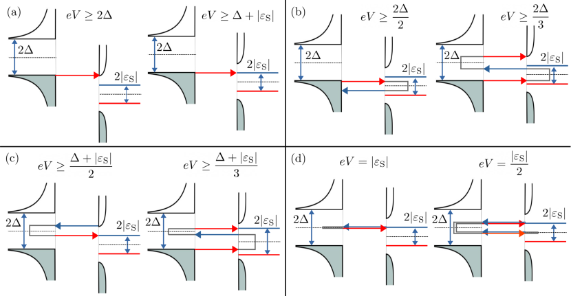
The second family of tunneling processes are the standard MARs, which are schematically represented in Fig. 9(b). These are MARs that start and end in the continuum of states of the electrodes. They contribute to the subgap structure by increasing the conductance at their threshold voltages with (this is the usual subharmonic gap structure in the absence of magnetism) and in every process a charge equal to is transferred. The absence of singularities in the LDOS of the impurity reduces the probability of the odd MARs like the one of order 3 shown on the right hand side in Fig. 9(b). More importantly, these MARs can give resonant contributions, where their probability is greatly enhanced, when during the cascade of reflections a quasiparticle hits the energy of a YSR state in the impurity. Thus, for instance, the probability of the second-order Andreev reflection in Fig. 9(b) is resonantly enhanced when . Notice that this is nothing else than the resonant Andreev reflection that was discussed in the previous section for a normal-conducting tip. Therefore, this Andreev reflection competes with the single-quasiparticle process connecting the continuum of the tip DOS with the YSR state and it eventually dominates the peak height at this bias when the junction transmission is sufficiently high. This competition was nicely discussed in Ref. Ruby2015 , both experimentally and theoretically. In a similar way, other standard MARs can become resonant at certain voltages. For instance, the third-order MAR in Fig. 9(b) is resonantly enhanced when , while . This implies that . At a first glance, this resonant condition might explain the appearance of the conductance peak at in Fig. 8. The alternative explanation of a peak due to thermally excited quasiparticles can be ruled out by the fact that such a peak would appear for any value of the YSR energy, which is not the case. The temperature in that example is simply too low for this quasiparticle process to give a significant contribution. Notice, however, that a closer inspection of Fig. 8 shows that the peak at extends up to , which suggests that another type of process is also at work in this case (see below).
Another family of Andreev reflections are those described in Fig. 9(c) in which a MAR either starts or ends in a YSR state. They give rise to the subgap structure at their threshold voltages with and they involve the transfer of charges across the junction. By comparing these processes with the standard MARs, we can see that, qualitatively speaking, the presence of the YSR states on the second superconducting contact reduces its “effective gap” such that quasiparticle states are present at instead of . On the other hand, since their probability critically depends on the DOS associated to a single YSR state, their contribution to the differential conductance depends on the bias polarity (see below discussion of Fig. 10). Moreover, there is a basic difference between even and odd MARs of this kind. Since the odd ones must connect the continuum of states of the tip, which does exhibit a BCS singularity, and a YSR state in the impurity, they can give rise to a negative differential conductance (NDC), which is actually what we see in Fig. 8. Signatures of the occurrence of these MARs have been reported experimentally in Refs. Randeria2016 ; Farinacci2018 . Let us also say that if there is some residual DOS inside the gap, for instance in the tip, one can also have MARs connecting the YSR states with that finite in-gap DOS. Thus, for instance, it is easy to convince oneself that it is possible to have such a second-order Andreev reflection connecting the lower YSR state and the residual DOS in the tip. This process has a threshold (positive) voltage and it is only possible as long as , which altogether implies that . We think that this is indeed the process that gives the main contribution to the conductance peak at in Fig. 8. In particular, this nicely explains why this peak is only visible for voltages .
Finally, we want to discuss a more exotic type of MAR that, in principle, could also exist in the presence of bound states. These MARs would start and end in a YSR bound state, see Fig. 9(d). Energetically speaking, these processes could occur at voltages with and they would involve the transfer of a charge equal to . Obviously, if they existed, their contribution would drastically depend on the bound state broadening and, given their resonant nature, they should give rise to a NDC. Given their hypothetical threshold voltages, it is tempting to assign the features that we see in Fig. 8 at and to the occurrence of these resonant MARs. However, a closer inspection of the diagrams of Fig. 9(d), and in particular of the spin of the quasiparticles involved in these processes, shows that these MARs require a bound state to have a finite DOS of both spin species, which is not the case for YSR states. So, in other words, these MARs are strictly forbidden due to the full spin polarization of the YSR bound states note2 . Then, the remaining question concerns the origin of the subgap structure at the energy of the YSR states and subharmonics of it. As discussed above, we think that the peak at in Fig. 8, which does not exhibit an NDC, is mainly due to a single-quasiparticle process. On the other hand, we attribute the peak at in Fig. 8 to the contribution of a second-order Andreev reflection connecting a YSR state and the residual DOS in the gap region on the impurity site. Such a process has precisely a threshold voltage . Let us say that we are not aware of any experimental observation of this latter conductance feature.
From our discussions above, we have concluded that the contributions to the differential conductance attributed to tunneling processes which either start or end in a single YSR state can depend on the bias polarity. To illustrate this fact, we show in Fig. 10 the results for the differential conductance in a case similar to that of Fig. 8, but in which the electron-hole is broken (). These results not only confirm our statement above, but they also show that the same series of conductance peaks appears in the subgap conductance when there is no electron-hole symmetry in the system.
V Discussion and conclusions
There are a number of ways in which this work could be extended. First of all, it would be desirable to extend the full counting statistics (FCS) theory of MARs to the case of magnetic impurities discussed in this work Cuevas2003 ; Cuevas2004 . The FCS technique allows us to unambiguously classify the tunneling processes according to the charge transferred. This could shed some additional light on the nature of the different transport processes in the complex situation investigated here. On the other hand, in many experiments several pairs of YSR states are reported. In this sense, it would be nice to study the interplay between different bound states and how this is reflected in the current-voltage characteristics for arbitrary transparency. In principle, this could be done within the framework of the Anderson model used in this work by including additional energy levels or orbitals in the impurity. Another interesting extension could be the analysis of the role of dynamical Coulomb blockade in our system. It is known that this dynamical effect, which results from the interaction of tunneling electrons with the electromagnetic environment, ultimately limits the energy resolution of tunneling experiments and it may have an important impact, especially, at very low temperatures Ast2016 . It would also be of great interest to study the role of electron correlations (beyond the mean field approximation used here) in all the transport properties discussed in this work. However, this is very challenging and it continues to be an important open problem Andersen2011 . Finally, our theory is ideally suited to describe the tunneling between magnetic impurities exhibiting their respective YSR states, which has been experimentally reported for the first time very recently Huang2019b . This is a problem that we shall tackle in a forthcoming paper.
So, to conclude, we have presented in this work a microscopic theory of the quantum transport through individual magnetic impurities coupled to superconductors. Motivated by recent STM-based experiments, we have studied the interplay between YSR states and (multiple) Andreev reflections in these systems with the help of a combination of a mean-field Anderson model and nonequilibrium Green’s function techniques. We have been able to identify the different tunneling processes and, in particular, we have predicted the occurrence of a large variety of Andreev reflections mediated by YSR states. Moreover, we have provided very precise guidelines on how to identify the contribution of these processes in actual experiments. From a more general perspective, our work provides further insight into spin-dependent Andreev transport that can also be of interest for the community of superconducting spintronics Linder2015 .
Acknowledgements.
The authors would like to thank Alfredo Levy Yeyati, Jakob Senkpiel, Robert Drost, Joachim Ankerhold, Ciprian Padurariu, and Björn Kubala for insightful discussions. A.V. and J.C.C. acknowledge funding from the Spanish Ministry of Economy and Competitiveness (MINECO) (contract No. FIS2017-84057-P). This work was funded in part by the ERC Consolidator Grant AbsoluteSpin (Grant No. 681164) and by the Center for Integrated Quantum Science and Technology (IQ). R.L.K., W.B., and G.R. acknowledge support by the DFG through SFB 767 and Grant No. RA 2810/1. J.C.C. also acknowledges support via the Mercator Program of the DFG in the frame of the SFB 767. †These authors contributed equally to this work.References
- (1) L. Yu, Bound state in superconductors with paramagnetic impurities, Acta Phys. Sin. 21, 75 (1965).
- (2) H. Shiba, Classical Spins in Superconductors, Prog. Theor. Phys. 40, 435 (1968).
- (3) A. I. Rusinov, Superconductivity near a paramagnetic impurity, Pis’Ma Zh. Eksp. Teor. Fiz. 9, 146 (1968) [JETP Lett. 9, 85 (1969)].
- (4) A. Yazdani, B. A. Jones, C. P. Lutz, M. F. Crommie, and D. M. Eigler, Probing the Local Effects of Magnetic Impurities on Superconductivity, Science 275, 1767 (1997).
- (5) S.-H. Ji, T. Zhang, Y.-S. Fu, X. Chen, X.-C. Ma, J. Li, W.-H. Duan, J.-F. Jia, and Q.-K. Xue, High-Resolution Scanning Tunneling Spectroscopy of Magnetic Impurity Induced Bound States in the Superconducting Gap of Pb Thin Films, Phys. Rev. Lett. 100, 226801 (2008).
- (6) K. J. Franke, G. Schulze, and J. I. Pascual, Competition of Superconducting Phenomena and Kondo Screening at the Nanoscale, Science 332, 940 (2011).
- (7) G. C. Ménard, S. Guissart, C. Brun, S. Pons, V. S. Stolyarov, F. Debontridder, M. V. Leclerc, E. Janod, L. Cario, D. Roditchev, P. Simon, and T. Cren, Coherent long-range magnetic bound states in a superconductor, Nat. Phys. 11, 1013 (2015).
- (8) M. Ruby, F. Pientka, Y. Peng, F. von Oppen, B. W. Heinrich, and K. J. Franke, Tunneling Processes into Localized Subgap States in Superconductors, Phys. Rev. Lett. 115, 087001 (2015).
- (9) N. Hatter, B. W. Heinrich, M. Ruby, J. I. Pascual, and K. J. Franke, Magnetic anisotropy in Shiba bound states across a quantum phase transition, Nat. Commun. 6, 8988 (2015).
- (10) M. Ruby, Y. Peng, F. von Oppen, B. W. Heinrich, and K. J. Franke, Orbital Picture of Yu-Shiba-Rusinov Multiplets, Phys. Rev. Lett. 117, 186801 (2016).
- (11) M. T. Randeria, B. E. Feldman, I. K. Drozdov, and A. Yazdani, Scanning Josephson spectroscopy on the atomic scale, Phys. Rev. B 93, 161115(R) (2016).
- (12) D. J. Choi, C. Rubio-Verdú, J. De Bruijckere, M. M. Ugeda, N. Lorente, and J. I. Pascual, Mapping the orbital structure of impurity bound states in a superconductor, Nat. Commun. 8, 15175 (2017).
- (13) L. Cornils, A. Kamlapure, L. Zhou, S. Pradhan, A. A. Khajetoorians, J. Fransson, J. Wiebe, and R. Wiesendanger, Spin-Resolved Spectroscopy of the Yu-Shiba-Rusinov States of Individual Atoms, Phys. Rev. Lett. 119, 197002 (2017).
- (14) N. Hatter, B. W. Heinrich, D. Rolf, and K. J. Franke, Scaling of Yu-Shiba-Rusinov energies in the weak-coupling Kondo regime, Nat. Commun. 8, 2016 (2017).
- (15) L. Farinacci, G. Ahmadi, G. Reecht, M. Ruby, N. Bogdanoff, O. Peters, B. W. Heinrich, F. von Oppen, and K. J. Franke, Tuning the Coupling of an Individual Magnetic Impurity to a Superconductor: Quantum Phase Transition and Transport, Phys. Rev. Lett. 121, 196803 (2018).
- (16) J. Brand, S. Gozdzik, N. Néel, J. L. Lado, J. Fernández-Rossier, and J. Kröger, Electron and Cooper-pair transport across a single magnetic molecule explored with a scanning tunneling microscope, Phys. Rev. B 97, 195429 (2018).
- (17) L. Malavolti, M. Briganti, M. Hänze, G. Serrano, I. Cimai, G. McMurtrie, E. Otero, P. Ohresser, F. Toi, M. Mannini, R. Sessoli, and S. Loth, Tunable Spin-Superconductor Coupling of Spin 1/2 Vanadyl Phthalocyanine Molecules, Nano Lett. 18, 7955 (2018).
- (18) S. Kezilebieke, R. Žitko, M. Dvorak, T. Ojanen, and P. Liljeroth, Observation of Coexistence of Yu-Shiba-Rusinov States and Spin-Flip Excitations, Nano Lett. 19, 4614 (2019).
- (19) J. Senkpiel, C. Rubio-Verdú, M. Etzkorn, R. Drost, L. M. Schoop, S. Dambach, C. Padurariu, B. Kubala, J. Ankerhold, C. R. Ast, and K. Kern, Robustness of Yu-Shiba-Rusinov resonances in the presence of a complex superconducting order parameter, Phys. Rev. B 100, 014502 (2019).
- (20) M. Etzkorn, M. Eltschka, B. Jäck, C. R. Ast, and K. Kern, Mapping of Yu-Shiba-Rusinov States from an Extended Scatterer, arXiv:1807.00646.
- (21) L. Schneider, M. Steinbrecher, L. Rózsa, J. Bouaziz, K. Palotás, M. dos Santos Dias, S. Lounis, J. Wiebe, and R. Wiesendanger, Magnetism and in-gap states of 3d transition metal atoms on superconducting Re, Quantum Mater. 4, 42 (2019).
- (22) E. Liebhaber, S. A. González, R. Baba, G. Reecht, B. W. Heinrich, S. Rohlf, K. Rossnagel, F. von Oppen, and K. J. Franke, Yu-Shiba-Rusinov States in the Charge-Density Modulated Superconductor NbSe2, Nano Lett. 20, 339 (2020).
- (23) H. Huang, R. Drost, J. Senkpiel, C. Padurariu, B. Kubala, A. Levy Yeyati, J.C. Cuevas, J. Ankerhold, K. Kern, C.R. Ast, Magnetic Impurities on Superconducting Surfaces: Phase Transitions and the Role of Impurity-Substrate Hybridization, arXiv:1912.05607.
- (24) H. Huang, C. Padurariu, J. Senkpiel, R. Drost, A. Levy Yeyati, J. C. Cuevas, B. Kubala, J. Ankerhold, K. Kern, C. R. Ast, Tunneling dynamics between superconducting bound states at the atomic limit, arXiv:1912.08901.
- (25) B. W. Heinrich, J. I. Pascual, and K. J. Franke, Single magnetic adsorbates on s-wave superconductors, Prog. Surf. Sci. 93, 1 (2018).
- (26) S. Nadj-Perge, I. K. Drozdov, J. Li, H. Chen, S. Jeon, J. Seo, A. H. MacDonald, B. A. Bernevig, A. Yazdani, Observation of Majorana Fermions in Ferromagnetic Atomic Chains on a Superconductor, Science 346, 602 (2014).
- (27) M. Ruby, F. Pientka, Y. Peng, F. von Oppen, B. W. Heinrich, K. J. Franke, End States and Subgap Structure in Proximity-Coupled Chains of Magnetic Adatoms, Phys. Rev. Lett. 115, 197204 (2015).
- (28) S. Kezilebieke, M. Dvorak, T. Ojanen, P. Liljeroth, Coupled Yu-Shiba-Rusinov states in molecular dimers on NbSe2, Nano Lett. 18, 2311 (2018).
- (29) M. Ruby, B. W. Heinrich, Y. Peng, F. von Oppen, K. J. Franke, Exploring a Proximity-Coupled Co Chain on Pb(110) as a Possible Majorana Platform, Nano Lett. 17, 4473 (2017).
- (30) M. Ruby, B. W. Heinrich, Y Peng, F. von Oppen, K. J. Franke, Wave-Function Hybridization in Yu-Shiba-Rusinov Dimers, Phys. Rev. Lett. 120, 156803 (2018).
- (31) D. Averin and D. Bardas, AC Josephson Effect in a Single Quantum Channel, Phys. Rev. Lett. 75, 1831 (1995).
- (32) J. C. Cuevas, A. Martín-Rodero, and A. Levy Yeyati, Hamiltonian approach to the transport properties of superconducting quantum point contacts, Phys. Rev. B 54, 7366 (1996).
- (33) E. Scheer, P. Joyez, D. Esteve, C. Urbina, and M. H. Devoret, Conduction Channel Transmissions of Atomic-Size Aluminum Contacts, Phys. Rev. Lett. 78, 3535 (1997).
- (34) E. Scheer, N. Agraït, J.C. Cuevas, A. Levy Yeyati, B. Ludoph, A. Martin-Rodero, G. Rubio Bollinger, J.M. van Ruitenbeek, and C. Urbina, The signature of chemical valence in the electrical conduction through a single-atom contact, Nature 394, 154 (1998).
- (35) B. M. Andersen, K. Flensberg, V. Koerting, and J. Paaske, Nonequilibrium Transport through a Spinful Quantum Dot with Superconducting Leads, Phys. Rev. Lett. 107, 256802 (2011).
- (36) The origin of this model is the following. Mean field calculations show that the spin degeneracy can be broken in presence of local Coulomb interaction for two (bare) spin degenerate levels. In the mean-field theory, the parameter and are calculated self-consistently. In our approach, we analyze the model in the parameter space of and .
- (37) J.-D. Pillet, C. H. L. Quay, P. Morn, C. Bena, A. Levy Yeyati, and P. Joyez, Andreev bound states in supercurrent-carrying carbon nanotubes revealed, Nat. Phys. 6, 965 (2010).
- (38) A. Martín-Rodero and A. Levy Yeyati, Josephson and Andreev transport through quantum dots, Adv. Phys. 60, 899 (2011).
- (39) A. Martín-Rodero and A. Levy Yeyati, The Andreev states of a superconducting quantum dot: mean field versus exact numerical results, J. Phys.: Condens. Matter. 24, 385303 (2012).
- (40) R. Žitko, J. S. Lim, R. López, and R. Aguado, Shiba states and zero-bias anomalies in the hybrid normal-superconductor Anderson model, Phys. Rev. B 91, 045441 (2015).
- (41) A. Kadlecová, M. Žonda, and T. Novotný, Quantum dot attached to superconducting leads: Relation between symmetric and asymmetric coupling, Phys. Rev. B 95, 195114 (2017).
- (42) R. Žitko, Quantum impurity models for magnetic adsorbates on superconductor surfaces, Physica B: Cond. Mat. 536, 230 (2018).
- (43) A. Kadlecová, M. Žonda, V. Pokorný, and T. Novotný, Practical Guide to Quantum Phase Transitions in Quantum-Dot-Based Tunable Josephson Junctions, Phys. Rev. Appl. 11, 044094 (2019).
- (44) M. I. Salkola, A. V. Balatsky, and J. R. Schrieffer, Spectral properties of quasiparticle excitations induced by magnetic moments in superconductors, Phys. Rev. B 55, 12648 (1997).
- (45) M. E. Flatté and J. M. Byers, Local electronic structure of defects in superconductors, Phys. Rev. B 56, 11213 (1997).
- (46) M. E. Flatté and J. M. Byers, Local electronic structure of a single magnetic impurity in a superconductor, Phys. Rev. Lett. 78, 3761 (1997).
- (47) A. V. Balatsky, I. Vekhter, and J. X. Zhu, Impurity-induced states in conventional and unconventional superconductors, Rev. Mod. Phys. 78, 373 (2006).
- (48) I. Martin and D. Mozyrsky, Nonequilibrium theory of tunneling into a localized state in a superconductor, Phys. Rev. B 90, 100508 (2014).
- (49) These processes could actually take place in presence of a spin-orbit interaction or if there are spin-flip tunneling processes in the junction as it happens in the case of two coupled magnetic impurities hosting noncollinear pairs of YSR bound states Huang2019b .
- (50) J.C. Cuevas and W. Belzig, Full Counting Statistics of Multiple Andreev Reflections, Phys. Rev. Lett. 91, 187001 (2003).
- (51) J.C. Cuevas and W. Belzig, DC-transport in superconducting point contacts: A full counting statistics view, Phys. Rev. B 70, 214512 (2004).
- (52) C. R. Ast, B. Jäck, J. Senkpiel, M. Eltschka, M. Etzkorn, J. Ankerhold, and K. Kern, Sensing the quantum limit in scanning tunnelling spectroscopy, Nat. Commun. 7, 13009 (2016).
- (53) J. Linder and J. W. A. Robinson, Superconducting spintronics, Nat. Phys. 11, 307 (2015).