Hyperbolicity in 2D transition metal ditellurides induced by electronic bands nesting
Abstract
Naturally occurring hyperbolic plasmonic media is rare, and was only recently observed in the 1T′ phase of WTe2. We elucidate on the physical origin of this strong infrared hyperbolic response, and attribute it to band-nested anisotropic interband transitions. Such phenomenon does not occur in general anisotropic materials, at least not in their pristine state. However, band-nested anisotropic interband transitions can in principle be induced via proper electronic band nesting. We illustrate this principle and demonstrate a topological elliptic-to-hyperbolic transition in MoTe2 via strain engineering, which is otherwise non-hyperbolic.
pacs:
71.20.Be, 52.25.Mq, 78.20.Jq, 78.67.-n, 73.90.+fIntroduction. Hyperbolic materials are characterized by anisotropic dielectric constants where the real parts of the principal components have opposite signs Poddubny et al. (2013); Nemilentsau et al. (2016). Such material accommodates modes with extremely large momentum, and exhibits a very high photonic density of states Zhang et al. (2012). Hence, such material can support directional polaritons Low et al. (2017) which belong to half-light and half-matter bosonic quasiparticles Liu et al. (2015); Kasprzak et al. (2006), enabling a series of potential applications, such as superlens Pendry (2000); Jacob et al. (2006); Smolyaninov et al. (2007); Fang et al. (2005), invisibility cloaks Pendry et al. (2006), nanowaveguide Cortes et al. (2012), and sub-diffractional resonators Guler et al. (2015). A practical approach creating hyperbolic media is to fabricate metal-dielectric structures Poddubny et al. (2013); Noginov et al. (2009) in which the components of the effective dielectric tensor can be engineered by tuning the constituent proportion and geometrical arrangement. Such man-made hyperbolic materials Low et al. (2017) suffer from high plasmonic loss in metal, complex nanofabrication requirement, optical resolution limited by the feature size, and are not electrically tunable.
Natural hyperbolic material would circumvent the above-mentioned limitations, and enable extreme confinement beyond what is possible with artificial man-made metamaterials. Layered 2D materials offer interesting opportunities on this front Low et al. (2017); Basov et al. (2016). A well-known example is hexagonal boron nitride, a naturally occurring hyperbolic material that sustains strongly confined phonon-polariton modes Caldwell et al. (2014); Li et al. (2015). The strong hyperbolic phonon polaritons were also discovered in the van der Waals (vdW) layered semiconductor -MoO3 Ma et al. (2018); Zheng et al. (2018, 2019), with accessible electromagnetic confinements up to two orders smaller than the corresponding photon wavelengths Zheng et al. (2018). In comparison with the metallic plasmon polaritons, the phonon polaritons possess the virtues of significantly reduced optical losses and much higher quality factors. However active control over phonon polaritons is challenging due to the insensitive lattice vibrations to external stimulus, which limits relevant applications in switchable nanophotonic devices.
Very recently, hyperbolic plasmonic signatures were experimentally observed in transition metal dichalcogenide (TMD) WTe2 Tang et al. (2017); Wang et al. (2020), a layered vdW material. The hyperbolic dispersion in the WTe2 thin film was also verified experimentally through far-field infrared absorption measurement Wang et al. (2020). Natural hyperbolic materials of plasmonic origin are rare, and this being the first experimental demonstration. Its physical origin to-date is also not known. Utilizing density function theory (DFT), we calculate the complex dielectric tensors of WTe2, and confirm the existence of this near-infrared hyperbolic regime observed in experiments. Through electronic bands and wavefunction analyses, we trace the origin of the emerging hyperbolicity to resonant anisotropic interband transitions via band nesting. We demonstrate this in another telluride material, MoTe2, where its pristine form is non-hyperbolic. Through band nesting engineering via strain, we induce a topological transition in MoTe2 from the elliptic to the hyperbolic regime. Hence, our work established the first electronic structure based approach to the engineering of natural hyperbolic materials and can be generally applied to other anisotropic 2D materials and their heterostructures.
Hyperbolic dielectric response. Bulk WTe2 has an orthorhombic crystal structure in its most energetically favorable state, commonly known as the phase Jiang et al. (2016). It features monolayer WTe2 structure of the 1T′ phase Fei et al. (2017) stacked on top of each other via weak vdW forces. The crystal structures for these layered WTe2 systems are displayed in Figs. 1(a)-1(c), for monolayer, bilayer, and trilayer respectively. The most stable layer stacking order is to rotate the alternate layers by 180o. In the simulation, periodic boundary condition is imposed in both in-plane and out-of-plane directions. For the latter, which is denoted as the z-axis, a 20 thickness vacuum layer is inserted to electronically isolate any interactions between supercells.
The calculated real parts of dielectric functions for monolayer, bilayer, and trilayer WTe2 are shown in Figs. 1(d)-1(f), and their respective imaginary parts are displayed in Figs. 1(g)-1(i). The subscript denotes the diagonal elements of the dielectric tensor. A material is generally classified as hyperbolic when . As shown in Fig. 1(d), the dielectric functions of monolayer WTe2 exhibit a strong anisotropic hyperbolic character at 1.0 eV, such that and . The hyperbolic spectral range resides in the near-infrared and is relatively unchanged, although it narrows, as the layer number increases from monolayer to trilayer as illustrated in Figs. 1(e) and 1(f). The trend continues such that in the bulk limit of WTe2, the material is no longer hyperbolic. This is qualitatively consistent with the experimental observation of hyperbolic response in thin film WTe2 in the infrared spectral range Wang et al. (2020).
Since the real and imaginary parts of the dielectric function are connected through the Kramers-Kronig relation Cardona and Peter (2005), it suffice to just consider the latter, due to the fact that is related to electronic losses, particularly interband transitions. For example, with a Lorentzian spectra with peak absorption at would have which admits a negative permittivity for frequencies larger than . Indeed, reveals strong resonant-like features at 1eV as shown in Figs. 1(g)-1(i). The oscillator strength (or spectral weight) of these resonances would dictates the degree of negative permittivity in as instructed by Kramers-Kronig relation.
As illustrated in Figs. 1(g)-1(i), the peaks at 1 eV in , which is responsible for the hyperbolicity, becomes weaker and broader as the layer thickness increases. This is consistent with the reduced negative permittivity in as reflected in Figs. 1(d)-1(f). The reducing spectral weight in with increasing layer thickness can be traced to the electronic wavefunction spread between the different layer space Li et al. (2014). As shown in Figs. S1-S3 in Supplementary Materials (SM), the wavefunctions of the top valence and bottom conduction bands in bilayer WTe2 are more disproportionately localized in one layer and delocalized between the layers, respectively, hence leading to reduced optical transition amplitudes compared to the monolayer counterpart.
Band nesting effect. To facilitate our discussion of the origin of hyperbolicity in WTe2, we focus on its monolayer and consider its dielectric response between the two bands above and below the Fermi level, denoted as and respectively. As shown in Fig. 2(a), the hyperbolic response is well captured by the optical transitions between and as indicated by the solid lines, where the full response is shown in dashed lines for comparison. As shown in Fig. 2(b), the intense peak in at 1eV can be traced to the interband transitions between and . Coincidentally, and display similar dispersions along the path, giving rise to a band nesting condition Carvalho et al. (2013) featured by . A consequence of band nesting is to induce a huge joint density of states (JDOS), since it is defined as , where Sk is the constant energy surface defined by const. Since the spectral weight of is proportional to the JDOS, the degree of band nesting in electronic bands of monolayer WTe2 would consequentially control the hyperbolicity. In order to visualize the landscape of band nesting within the Brillouin zone, , and are shown in Fig. 2(c). Besides the -Y path, band nesting also occurs in other regions of the -space as indicated by the iso-energy dashed lines shown in Fig. 2(c). It should be noted that the energy difference between the nested bands is 1eV, coinciding with the hyperbolic spectral range.
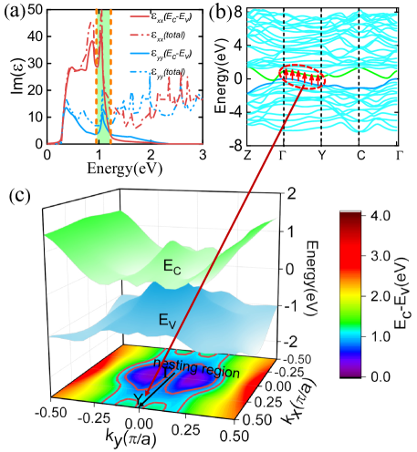
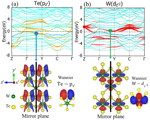
Anisotropic opitcal transition. The band nesting phenomenon in monolayer WTe2 is responsible for the ‘resonant-like’ interband transition at 1eV, and accounts for the appearance of negative at energy larger than 1eV. However, the anisotropic character of in-plane dielectric tensors is also a pre-requisite to attain hyperbolicity. In fact, the strength of imaginary part of dielectric function is a product of JDOS and the electric dipole transition moment matrix. The electric dipole moment matrix is expressed as , where and are wavefunctions of and , and is the position operator. The symmetry and space orientation of and would impose constraints on the optical transition selection rules Yuan et al. (2015); Hotta (2018), and is responsible for inducing anisotropic dielectric tensors. The band is mainly composed of orbital on Te atoms and the band is formed by , , and orbitals on W atoms (see in Figs. S4 and S5 in SM.). Here the orbitals are defined in the coordinate frame by crystallographic space group notation. The relationships between crystallographic coordinate frame and previous defined conventional coordinate frame are , , and . Due to the symmetry of the wavefunctions, the transition matrix elements and are zero, and only W- and Te- orbital projected bands produce finite electric dipole transitions (see Fig. 3). The wavefunctions of and states in the band nesting region are also displayed at the bottom of Fig. 3, which are mainly composed of Te--like and W--like orbitals, in agreement with the maximum localized Wannier functions analysis.
We proceed to discuss the optical selection rules for electric dipole transition. The crystal structure has a mirror plane symmetry define by the = 0 plane, and the and wavefunctions in the -path exhibit odd and even parities with respect to this mirror plane. As a result, the electric dipole transition is symmetry allowed in direction, while the transition in direction is forbidden under the mirror plane restriction. Hence, this selection rule ensures that the band-nested optical transitions occur only for z′(or x) polarized excitations. However, this symmetry constraint will be somewhat relaxed in the band-nesting region of k-space off the high symmetry path. Despite this, both Te--like and W--like content in the and wavefunction respectively, exhibit strong space orientation in direction. Hence, this also attributes to the larger amplitude of transition element than . These symmetry constraints in conjunction with the orbital type underlie the strong in-plane anisotropic dielectric tensors. Furthermore, we also verified our proposed mechanism in crystal-field coordinate frame which has been widely used to investigate optical transitions in transition metal coordination complexes (see SM text).
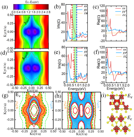
Band nesting modulation. The proposed principle of band nesting induced hyperbolic dielectric response should be generally applicable to anisotropic materials. To demonstrate this, we consider the monolayer MoTe2 system, a sister compound of WTe2, which also possesses stable 1T′ phase Naylor et al. (2016). Figs. 4(a)-4(c) display the band nesting contour for across the Brillouin zone and the corresponding and for monolayer MoTe2 respectively. Unlike WTe2, monolayer MoTe2 is not hyperbolic in its pristine state across the energy range as shown in green background. Although also exhibits similar resonant-like features as shown in Fig. 4(b), it is somewhat broadened in energy, as indicated by the green highlighted background. Its lower and upper energy limits correspond to the red and blue contour lines in Fig. 4(a). The center of the second resonant feature in of monolayer MoTe2 is localized around 0.6 eV, however the band nesting corresponding to this energy region is poor, which is manifested by relatively large k-space area bounded by the red and blue contour lines in Fig. 4(a), which herein denoted as Anest. Conversely, Anest should be zero for perfectly nested bands across the whole Brillouin zone.
The electronic structure of MoTe2 near the Fermi level is determined by Mo-4 and Te-5 orbitals, and their hybridization is also responsible for the Mo-Te chemical bond. Hence, the electronic structure is tunable through strain engineering. The band nesting contour, , and for monolayer MoTe2 under 2% tensile strain are shown in Figs. 4(d)-4(f). The band nesting profile and dielectric functions of the strained monolayer MoTe2 display evident alterations in comparison with the unstrained one. The strained monolayer MoTe2 exhibits hyperbolic response at 0.8 eV, see Fig. 4(f). Evidently, the band nesting region around the energy range where the hyperbolicity occurs is appreciably enlarged, while that of Anest is reduced, see Fig. 4(d), resulting in a higher quality peak in as shown in Fig. 4(e).
Finally, we examine how the mechanical strain modulates the band dispersions of and which in turn enhances the degree of band nesting. As indicated in Figs. 4(a) and 4(d), the band nesting does not occur along common high symmetry lines as in the case of WTe2. Hence, we depict the band dispersion of and for the unstrained case across the momentum space of interest as shown in Figs. 4(g) and 4(h) respectively. In particular, we highlighted in blue the region of -space corresponding to the energy window of interest responsible for the resonant-like feature in and the emergent hyperbolicity. In comparison with , band is more dispersive, indicative by the smaller area of the blue shaded region.
We found that the application of strain has a prominent effect on the dispersion of . As shown in Fig. 4(g), the application of 2% tensile strain appreciably reduces the dispersion of , hence increasing the -space area corresponding to this energy window, as indicated by the shaded orange region. The increased in -space area, in conjunction with the relatively non-dispersive and bands, results in band nested interband transitions. The partial charge densities extracted from the electronic states in the above considered energy ranges are shown in Fig. 4(i), which display a mixing of orbital components on Te atoms and orbital components on Mo atoms for but only orbital components on Mo atoms for . The band dispersion is determined by the overlap and mixing of atomic orbitals on neighboring crystal sites Zeier et al. (2016). In monolayer MoTe2, the orbital mixed component displays a larger overlap between neighboring crystal sites than the one including orbital only as shown in Fig. 4(i). Therefore, the electronic state of should exhibit a stronger dispersion than that of in our specified energy region. The application of tensile strain reduces the orbital overlap, hence resulting in weaker band dispersion for . On the contrary, the interplay of on-site orbital components related to is less affected by strain.
Summary. In summary, we elucidate the physical origin of the hyperbolicity in WTe2, attributing it to the band nesting effect in conjunction with highly anisotropic optical transition dipole. Guided with this understanding, we applied electronic band nesting engineering to another TMD, MoTe2, and successfully demonstrate elliptic to hyperbolic transition through strain engineering. We envision that natural 2D hyperbolic materials can be made widely available through electronic band engineering via the band nesting approach as outlined in this work.
Acknowledgements.
Acknowledgment. HW and TL acknowledge funding support from NSF/DMREF under Grant Agreement No. 1921629.∗ To whom correspondence should be addressed: tlow@umn.edu.References
- Poddubny et al. (2013) A. Poddubny, I. Iorsh, P. Belov, and Y. Kivshar, Nat. Photonics 7, 948 (2013).
- Nemilentsau et al. (2016) A. Nemilentsau, T. Low, and G. Hanson, Phys. Rev. Lett. 116, 066804 (2016).
- Zhang et al. (2012) J. Zhang, L. Zhang, and W. Xu, J. Phys. D: Appl. Phys. 45, 113001 (2012).
- Low et al. (2017) T. Low, A. Chaves, J. D. Caldwell, A. Kumar, N. X. Fang, P. Avouris, T. F. Heinz, F. Guinea, L. Martin-Moreno, and F. Koppens, Nat. Mater. 16, 182 (2017).
- Liu et al. (2015) X. Liu, T. Galfsky, Z. Sun, F. Xia, E.-c. Lin, Y.-H. Lee, S. Kéna-Cohen, and V. M. Menon, Nat. Photonics 9, 30 (2015).
- Kasprzak et al. (2006) J. Kasprzak, M. Richard, S. Kundermann, A. Baas, P. Jeambrun, J. Keeling, F. Marchetti, M. Szymańska, R. André, J. Staehli, et al., Nature 443, 409 (2006).
- Pendry (2000) J. B. Pendry, Phys. Rev. Lett. 85, 3966 (2000).
- Jacob et al. (2006) Z. Jacob, L. V. Alekseyev, and E. Narimanov, Opt. Express 14, 8247 (2006).
- Smolyaninov et al. (2007) I. I. Smolyaninov, Y.-J. Hung, and C. C. Davis, Science 315, 1699 (2007).
- Fang et al. (2005) N. Fang, H. Lee, C. Sun, and X. Zhang, Science 308, 534 (2005).
- Pendry et al. (2006) J. B. Pendry, D. Schurig, and D. R. Smith, Science 312, 1780 (2006).
- Cortes et al. (2012) C. Cortes, W. Newman, S. Molesky, and Z. Jacob, J. Opt. 14, 063001 (2012).
- Guler et al. (2015) U. Guler, V. M. Shalaev, and A. Boltasseva, Mater. Today 18, 227 (2015).
- Noginov et al. (2009) M. Noginov, Y. A. Barnakov, G. Zhu, T. Tumkur, H. Li, and E. Narimanov, Appl. Phys. Lett 94, 151105 (2009).
- Basov et al. (2016) D. Basov, M. Fogler, and F. G. De Abajo, Science 354, aag1992 (2016).
- Caldwell et al. (2014) J. D. Caldwell, A. V. Kretinin, Y. Chen, V. Giannini, M. M. Fogler, Y. Francescato, C. T. Ellis, J. G. Tischler, C. R. Woods, A. J. Giles, et al., Nat. Commun. 5, 1 (2014).
- Li et al. (2015) P. Li, M. Lewin, A. V. Kretinin, J. D. Caldwell, K. S. Novoselov, T. Taniguchi, K. Watanabe, F. Gaussmann, and T. Taubner, Nat. Commun. 6, 1 (2015).
- Ma et al. (2018) W. Ma, P. Alonso-González, S. Li, A. Y. Nikitin, J. Yuan, J. Martín-Sánchez, J. Taboada-Gutiérrez, I. Amenabar, P. Li, S. Vélez, et al., Nature 562, 557 (2018).
- Zheng et al. (2018) Z. Zheng, J. Chen, Y. Wang, X. Wang, X. Chen, P. Liu, J. Xu, W. Xie, H. Chen, S. Deng, et al., Adv. Mater. 30, 1705318 (2018).
- Zheng et al. (2019) Z. Zheng, N. Xu, S. L. Oscurato, M. Tamagnone, F. Sun, Y. Jiang, Y. Ke, J. Chen, W. Huang, W. L. Wilson, et al., Sci. Adv. 5, eaav8690 (2019).
- Tang et al. (2017) S. Tang, C. Zhang, D. Wong, Z. Pedramrazi, H.-Z. Tsai, C. Jia, B. Moritz, M. Claassen, H. Ryu, S. Kahn, et al., Nat. Phys. 13, 683 (2017).
- Wang et al. (2020) C. Wang, S. Huang, Q. Xing, Y. Xie, C. Song, F. Wang, and H. Yan, Nat. Commun. 11, 1 (2020).
- Jiang et al. (2016) Y. Jiang, J. Gao, and L. Wang, Sci. Rep. 6, 1 (2016).
- Fei et al. (2017) Z. Fei, T. Palomaki, S. Wu, W. Zhao, X. Cai, B. Sun, P. Nguyen, J. Finney, X. Xu, and D. H. Cobden, Nat. Phys. 13, 677 (2017).
- Cardona and Peter (2005) M. Cardona and Y. Y. Peter, Fundamentals of semiconductors (Springer, 2005).
- Li et al. (2014) Y. Li, A. Chernikov, X. Zhang, A. Rigosi, H. M. Hill, A. M. Van Der Zande, D. A. Chenet, E.-M. Shih, J. Hone, and T. F. Heinz, Phys. Rev. B 90, 205422 (2014).
- Carvalho et al. (2013) A. Carvalho, R. Ribeiro, and A. C. Neto, Phys. Rev. B 88, 115205 (2013).
- Yuan et al. (2015) H. Yuan, X. Liu, F. Afshinmanesh, W. Li, G. Xu, J. Sun, B. Lian, A. G. Curto, G. Ye, Y. Hikita, et al., Nat. Nanotechnol. 10, 707 (2015).
- Hotta (2018) S. Hotta, Mathematical Physical Chemistry (Springer, 2018).
- Naylor et al. (2016) C. H. Naylor, W. M. Parkin, J. Ping, Z. Gao, Y. R. Zhou, Y. Kim, F. Streller, R. W. Carpick, A. M. Rappe, M. Drndic, et al., Nano Lett. 16, 4297 (2016).
- Zeier et al. (2016) W. G. Zeier, A. Zevalkink, Z. M. Gibbs, G. Hautier, M. G. Kanatzidis, and G. J. Snyder, Angew. Chem. Int. Ed. 55, 6826 (2016).