X-ray phase contrast topography to measure the surface stress and bulk strain in a silicon crystal
Abstract
The measurement of the Si lattice parameter by x-ray interferometry assumes the use of strain-free crystals, which might not be true because of intrinsic stresses due to surface relaxation, reconstruction, and oxidation. We used x-ray phase-contrast topography to investigate the strain sensitivity to the finishing, annealing, and coating of the interferometer crystals. We assessed the topography capabilities by measuring the lattice strain due to films of copper deposited on the interferometer mirror-crystal. A byproduct has been the measurement of the surface stresses after complete relaxation of the coatings.
1 Introduction
We used a single-crystal x-ray interferometer to measure the lattice parameter of silicon to within a fractional uncertainty approaching 1 nm/m [1]. The interferometer was ground by diamond tools and chemically etched to remove the surface damage [2]. If too little material is etched away, lattice strains prevent the interferometer operation; if too much, the interferometer geometry degrades, and the fringe contrast is lost.
Phase-contrast topography by x-ray interferometry is a well known tool to study defects and strains in single crystals [3, 4, 5, 6, 7]. We used it to investigate the effect of the surface finishing on the interferometer operation [8]. Our goal was to optimize the manufacturing and to trade-off between no surface damage (via chemical etching) and accurate geometry (via mechanical grinding). The test interferometers were etched step-by-step and etching was stopped when it neither improved the fringe contrast nor reduce the lattice strain. The procedure that was found optimal prescribes a first chemical etching, then machining with the finest grit size to correct about 10 m etch errors, and a final etching for a depth of about 50 m.
These investigations did not give certainties that surface stresses due to oxidation, relaxation, and reconstruction did not affect the lattice-parameter value. The magnitude of this error was estimated by a finite element analysis, where the surface stress (a fundamental property of the crystal interface with the environment) was modelled by an elastic membrane having a hypothetical 1 N/m tensile strength [9]. We also calculated the surface stress by the density functional theory [10] and found a value exceeding 1 N/m, which value potentially jeopardizes the measurement accuracy.
Prompted by this treat and the observations of increased visibility and reduced strains after annealing reported in [11, 12], we carried out new topographic investigations of the annealing and etching effects of the interferometer crystals. To test the capabilities of phase-contrast topography, we measured the strain in the crystal bulk caused by nanometric films of copper deposited on one of the interferometer crystals. As a byproduct, we obtained the in-plane mean-stress in copper films on a silicon substrate.
Phase-contrast imaging proved to be an extremely sensitive technique to measure stress in films, only a few nanometres thick. Since it affects the design, processing, performance, reliability, and lifetime of advanced materials and components, the measurement of stress in thin films and coatings is also a crucial issue in materials science and technology [13, 14].
2 Experimental set-up
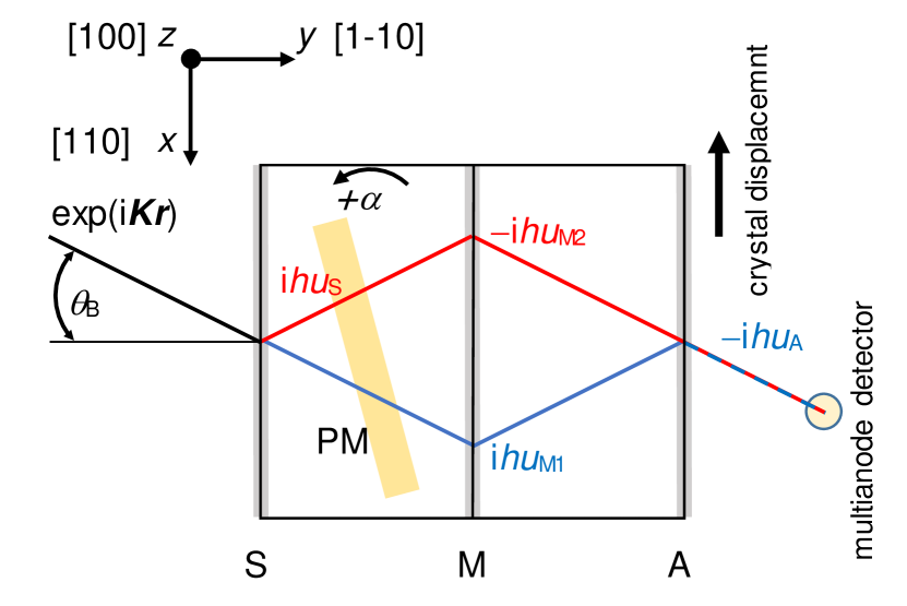
Figure 1 shows the apparatus for phase-contrast topography. A first crystal (splitter) splits 17 keV x-rays from a fixed anode mm2 Mo K source, which are recombined, via a mirror-like crystal, by the third (analyser). X-rays are roughly collimated by a mm2 slit placed in front of the interferometer. The interference fringes are imaged onto a multianode photomultiplier tube through a vertical 15 mm pile of eight 1 mm NaI(Tl) scintillators, spaced by 1 mm shades.
The interferometer blades (splitter, mirror, and analyser) are mm3, spaced 10 mm apart, and protrude from a common base (see Fig. 2). Since the x-ray source and detector are 0.8 m and 0.3 m apart from the mirror and the beams’ width at the mirror is 1 mm, the images of the scintillator pixels projected on the mirror are, on the average, mm2. The projected image of the 15 mm scintillator pile is 13 mm height, from the mirror top downward.
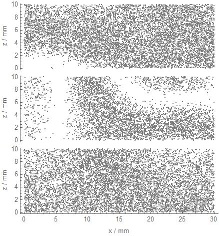
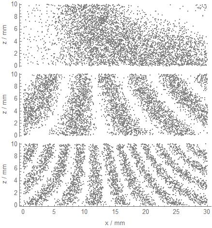
As shown in Fig. 1, we surveyed the moiré pattern by shifting the interferometer in 0.5 mm steps along the -axis and detecting the interference fringes in 61 adjacent mm2 vertical (overlapping) slabs subdivided into 8 (overlapping) pixels mm2. Therefore, the pixels survey a mm2 area, by using the coordinates of the pixel centres.

3 Measurement equation
In a geometric-optics model of the interferometer operation (with the positive-exponent choice representing a plane wave with positive wave number , see Fig. 1), each reflection delays the x-ray phase by [15, 16], where is the reciprocal vector, is the diffracting-plane spacing, is the component of the displacement field of the splitter-, mirror-, or analyzer-lattice. The sign is positive if the displacement occurs in the same direction as the -component of the incident-beam wave vector and negative otherwise. No phase delay occurs in the transmissions.
The phase delays along the two paths reaching the observation plane – one performing two reflections (R) followed by one transmission (T), the other one transmission followed by two reflections – are thus
| (1a) | |||||
| (1b) | |||||
An interference occurs because the rays overlap after crossing crystal lattices whose planes are misplaced one to the other. The total phase is
| (2) |
A phase modulator, plastic sheet 1 mm thick, is placed between the splitter and mirror. A simple geometrical analysis shows that – with the positive-exponent choice to represent a plane wave with positive (see Fig. 1) – it varies the interference phase by
where is the angle of rotation, the thickness of the modulator, the length of the X-ray path through the modulator, the index of refraction, the Bragg angle and the linearization with respect to the rotation angle is valid if rad.
When the phase modulator is rotated, the moving fringes are detected by each of the eight photomultiplier channels, making it possible to extract the effective displacement field . The measurement equation is
| (3) |
where label the image pixel, is the average count rate, the contrast, and the period.
The phases in the image pixels were recovered by (non-linear) least-squares estimations, with the and constraints. After unwrapping, we found the optimal polynomial regression explaining the data and used it to infer the effective lattice displacement . The trade-off between underfitting and overfitting was carried out according to [17, 18]. Eventually, we calculated the components (normal strain, the relative variation of lattice spacing), and (shear strain, the lattice-plane rotations about the -axis) of the strain tensor.
Since the fringes phase is recovered only modulo , a constant field is undetectable. However, positive phase gradients correspond to displacements of the splitter and analyser lattices in the -direction of the incident x-rays. The opposite is true for the mirror lattice. Therefore, tensile and compressive strains can be distinguished.
In (2), we neglected minor contributions to the phase, coming from deviations from ideally plane and parallel surfaces of the crystals and phase modulator. They are discussed in [16, 8] and might amount to a few per cent of a period. However, since we are interested in the strain changes after reprocessing of the crystal surfaces, we are looking at the difference of subsequent phase surveys and these constant contributions are mostly irrelevant.
4 Crystal annealing
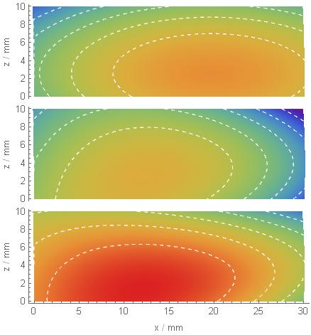
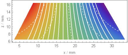
We surveyed the lattice strain of the interferometer crystals after optimal grinding and etching. Next, the interferometer was annealed in an evacuated tube furnace (the residual pressure was mbar), at 800 ∘C for 12 h. Eventually, the finishing of the crystal surfaces was reset by re-etching. The sequence of moiré topographies is shown in Fig. 3.
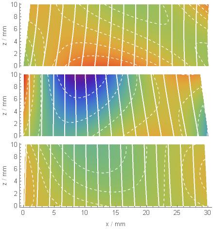
After finding the optimal approximations of the lattice-displacement fields (the residual standard deviations are about 3% of the peak-to-peak displacements), we calculated the and components of the strain tensors. Figures 4 and 5 highlight that the surface finishing plays a role in determining the bulk spacing and tilt of the diffracting planes. Sorted as in Figs. from 3 to 5, the mean strains and peak-to-peak variations are
| (4) |
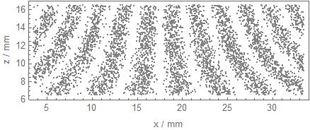
While the normal strain did not change significantly, there was an overall alignment of the diffracting planes, indicating that some stress in the base was relieved. Figure 6 shows that the realignment of the interferometer crystals was significant enough to improve the fringe contrast.
Since, according to (2), four displacement fields superimpose, we cannot give a measure of the strain in any single crystal. If we assume the four fields uncorrelated, by dividing the observed peak-to-peak strains by two, we can estimate a (local) surface effects on the spacing and tilt of the diffracting planes of about nm/m and nrad.
5 Crystal coating
To check the capabilities of phase-contrast topography and to gain some preliminary clues on the possible effects of the SiO2 surface layer on the lattice parameter, we measured the crystal strain after auto-catalytical coatings of the mirror surface with nanometric films of copper.
The coating (see Fig. 2) was carried out by an electroless galvanic displacement mechanism in a water solution of copper (II) nitrate, ( g L-1), and ammonium fluoride, ( g L-1). In this process, the copper plates the silicon surface and, simultaneously, the oxidised silicon is removed by to form water-soluble silicates and a clean interface between the Cu layer and the silicon crystal surface. Therefore, two processes go along: etching of the silicon surface and plating by copper. The overall stoichiometric reaction is [21]
| (5) |
The growth rate and quality of the Cu film depend on the solution composition and temperature. Therefore, we standardised them as well as the plating duration, 10 s, 20 s, and 40 s.
5.1 Film-thickness measurement
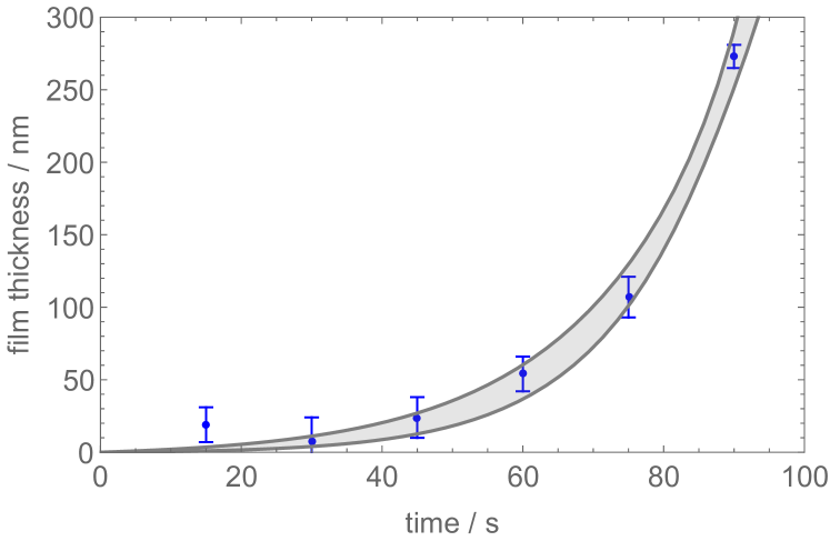
We measured the thickness of the Cu film by coating an optical polished single-crystal Si wafer whose surface was masked to coat (with times ranging from 15 s to 90 s with 15 s increments) six mm2 Cu pads, each bounded by a reference Cu-free area.
After the Cu films were removed by a water solution of iron(III) chloride, FeCl3 ( g L-1), we used an optical confocal profilometer (Sensofar S Neox Optical Profiler) to measure the steps between the coated and non-coated areas. Since the Cu molar volume is half that of Si and – according to (5) – two Cu atoms are a substitute for each Si atom removed, the thickness of the Cu films were estimated as equal to the observed drops. Figure 7 shows the results.
We prepared the mirror surface by the same etching/coating procedure used for the Si wafer: three increasing deposition time (10 s, 20 s, 40 s) were used to plate the surface with an increasingly thicker copper film. According to Fig.7, we estimated the thicknesses of the Cu-films on the interferometer mirror as equal to nm, nm, and nm, respectively. The parentheses are a concise notation for the standard uncertainty; the enclosed digit applies to the numeral left of themselves.
5.2 Displacement-field measurement.
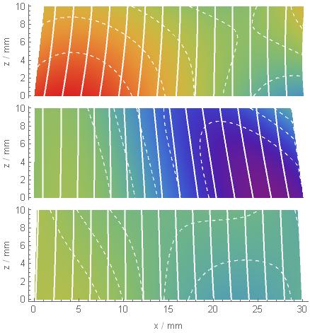
The displacements of the mirror lattice due to the Cu coatings, , were obtained by subtracting the regression of the pre-coating displacement field from those observed after the coatings, and reversing the sign.
The moiré topographies and displacement fields are shown in Figs. 8 and 9. The Cu films compress the crystal lattice and the stress increases with the thickness. This compression is consistent with the tensile stress of the Cu films (developing after growing and relaxation) reported in the literature [13, 14].
5.3 Surface-stress measurement
To infer the magnitude of the tensile stress of the Cu film, we set up a finite element analysis of the interferometer mirror, modelled as a mm3 Si crystal [22]. The effect of the film tensile-stress – assumed equiaxial and uniform – was simulated by a compressive surface-stress, , modelled as forces per unit length (from N/m to N/m, in variable steps), applied orthogonally to its 12 edges and lying in the crystal surfaces. Also, we set Dirichlet boundary conditions on the bottom surface, specifying null displacements, and used an anisotropic stiffness matrix [9].
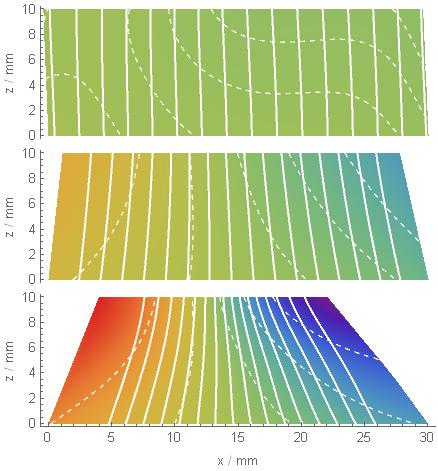
To realise a digital twin of the experimental set-up, the lattice displacement along the axis obtained via the finite element analysis, , was averaged over a pair of mm2 windows spaced by 4 mm, the separation of the x-ray paths at the interferometer mirror (see Fig. 1). To simulate the experimental images, the window pairs (the image of each scintillator pixel) were shifted vertically by eight 1.25 mm steps and horizontally by sixty-one 0.5 mm steps. Eventually, we found the polynomial regressions explaining the simulated data trading-off again between underfitting and overfitting according to [17, 18]. The regression of the displacement field for the N/m case is shown in Fig. 10. Figure 11 shows the moiré topography inferred from this regression.
The similarities between the displacements and fringes depicted in Figs. 10 and 11 and the ones at the bottom of Figs. 8 and 9 are a clear hint that a surface stress of a few N/m is the quantity driving the observed strain of the crystal lattice. The strain magnitude is proportional to the density of the fringes, showing that the digital twin predicts correctly that the crystal is more strained at the free top and that the strain degrades at the bottom, where the crystal base hinders the lattice distortion. With a digital twin at hand that predicts the deformation of the crystal, we determined the magnitude and sign of the surface stress originated by the copper film and its dependence on the thickness.
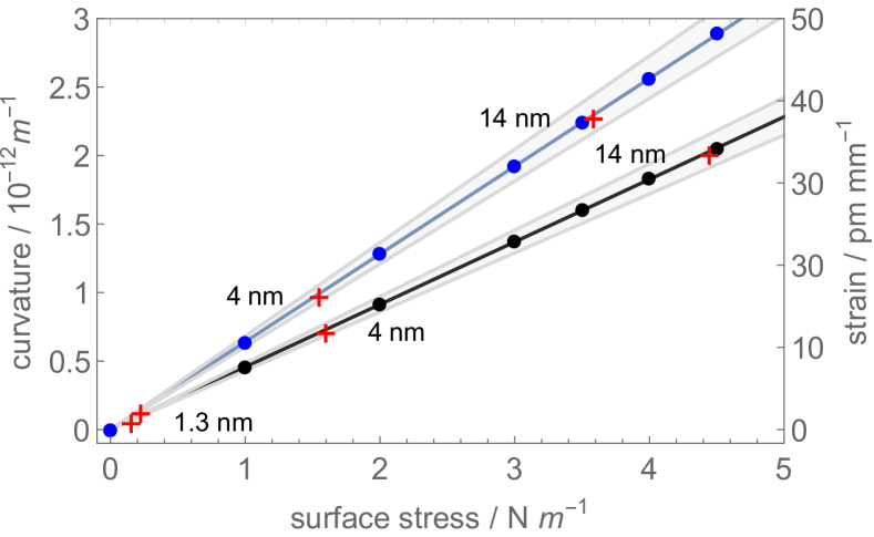
The surface stress was estimated by using the mean strains observed at the mirror top – , where mm is the length of the moiré images – in the nomogram shown in Fig. 12 (black line), which gives the same mean strains evaluated using the digital-twin data as a function of the surface stress. The values of the mean stress obtained via the optimal regression of the data,
| (6) |
where the standard uncertainties were estimated as and is the standard deviation of the residuals, led to
| (7) |
The simulated displacements are well approximated by (rectangular) hyperbolic paraboloids, having the axes rotated by 45∘ clockwise with respect to the and axes. They are quadratic surfaces given by the equation
| (8) |
where mm are the coordinates of the centre, is the surface stress, and and are the displacement and Gaussian curvature in the centre.
The axes of the paraboloids approximating the experimental data might be slightly rotated to those approximating the simulated ones, and their centres displaced somewhat. While the and axes of the finite element model are parallel to the crystallographic directions (110) and (001), the axes experimentally determined might be rotated, might deviate from being orthogonal, and their origin might be displaced. Furthermore, the assumption of uniform surface stress might not be valid.
To accommodate these degrees of freedom, we observed that Gaussian curvature is the only parameter of (8) depending on the surface stress. Also, as shown in Fig. 12, depends linearly on .
Furthermore, it is invariant under distance-preserving transformations allowing thus to compare misaligned paraboloids. This fact enables to be estimated via the Gaussian curvatures of the paraboloids best fitting the experimental data.
Therefore, to take the possible misalignments between the set-up and finite-element model into account, we modelled the experimental images as
and calculated the curvatures as , where is the Hessian of (5.3), and the vertical bars indicate the determinant. The results are
| (10) |
where the standard uncertainty of the (5.3) residuals was propagated through the calculations also considering that, because of the pixel overlapping, the independent data are only a one-eight of the total. Eventually, we used the estimated curvatures in the nomogram, as shown in Fig. 12 (blue line), and found the abscissae
| (11) |
corresponding to the curvatures listed in (10). This procedure favours the values that ensure the best overlapping (under a distance-preserving transformation) between the contour lines of the observed and simulated displacement fields.
The standard uncertainties associated with our estimates (7) and (11) take only the statistical dispersion of the phase data into account. A more realistic 10% fractional uncertainty follows from the comparison of the estimates based on the mean strain and strain-field curvature.
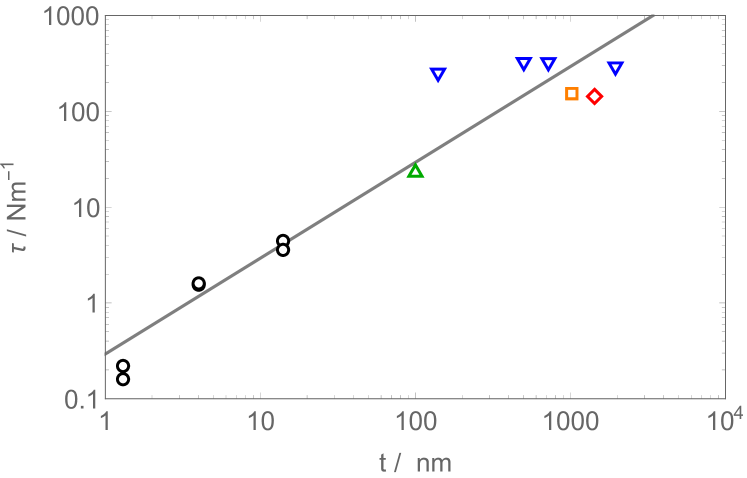
A survey of the literature suggests that almost three orders of magnitude can be extrapolated from observed dependence of the surface stress on the film thickness. Figure 13 compares our surface stress values with the stress-thicknesses of Cu films on acrylonitrile butadiene styrene, metals, and SiO2 [13, 14]. According to the linear regression of our data, the mean in-plane stress in the Cu film, 0.29(2) GPa, is independent of the film thickness.
6 Conclusion
The accurate measurement of the silicon lattice parameter by x-ray interferometry was a crucial step in counting the atoms in Si spheres – via their unit-cell volumes – for the determination of the Avogadro and Planck constants. It is now essential to the kilogram realisation, by reversing the count.
For a 1 kg Si sphere, the effect of the surface stress on the lattice parameter is irrelevant. However, it might be not so for the x-ray interferometer crystals, which, typically, are only 1 mm thick. This fact might harm the accuracy of the lattice parameter and unit-cell volume.
We have shown, via phase-contrast imaging of the crystal-lattice strains, that the surface finishing has measurable effects on the strain field of the diffracting planes, at the level of few parts per .
We coated one of the interferometer crystals with nanometric Cu films, detected the strains of the diffracting planes, and determined the surface stresses explaining them. The resulting mean in-plane stress in the Cu films, 0.29(2) GPa, is consistent with the stress-thickness values given in the literature for similar interfaces [13, 14]. We also observe that the strains caused by nanometric Cu films support our fractional 1.25(72) nm/m correction of the measured lattice-parameter [19, 20].
Phase-contrast imaging by x-ray interferometry can be used to determine the stress in different films on silicon. Nanometric SiO2 films better represent the interface of the interferometer crystals, a reconstructed Si layer and an oxide film. Therefore, future work will aim at growing SiO2 films having known thickness and at measuring the associated diffracting-plane strain.
References
- [1] E. Massa, C. P. Sasso, G. Mana, and C. Palmisano. A more accurate measurement of the 28si lattice parameter. Journal of Physical and Chemical Reference Data, 44(3):031208, 2015.
- [2] M. Zawisky, J. Springer, R. Farthofer, and U. Kuetgens. A large-area perfect crystal neutron interferometer optimized for coherent beam-deflection experiments: Preparation and performance. Nuclear Instruments and Methods in Physics Research Section A: Accelerators, Spectrometers, Detectors and Associated Equipment, 612(2):338 – 344, 2010.
- [3] U. U. Bonse, W. Graeff, and G. Materlik. X-ray interferometry and lattice parameter investigation. Rev. Phys. Appl., 11(1):83–87, 1976.
- [4] M. Ohler, S. Koehler, and J. Haertwig. X-ray diffraction moiré topography as a means to reconstruct relative displacement fields in weakly deformed bicrystals. Acta Crystallographica Section A, 55(3):423–432, 1999.
- [5] I M Fodchuk and N D Raransky. Moir images simulation of strains in x-ray interferometry. Journal of Physics D: Applied Physics, 36(10A):A55–A59, 2003.
- [6] D. A. Pushin, D. G. Cory, M. Arif, D. L. Jacobson, and M. G. Huber. Reciprocal space approaches to neutron imaging. Applied Physics Letters, 90(22):224104, 2007.
- [7] H Miao, A Panna, A Gomella, E Bennett, S Znati, L Chen, and H Wen. A universal moiré effect and application in x-ray phase-contrast imaging. Nature Physics, 12:830–834, 2016.
- [8] A Bergamin, G Cavagnero, G Mana, E Massa, and G Zosi. Measuring small lattice distortions in si-crystals by phase-contrast x-ray topography. Journal of Physics D: Applied Physics, 33(21):2678–2682, 2000.
- [9] D Quagliotti, G Mana, E Massa, C Sasso, and U Kuetgens. A finite element analysis of surface-stress effects on measurement of the si lattice parameter. Metrologia, 50(3):243–248, 2013.
- [10] C Melis, S Giordano, L Colombo, and G Mana. Density functional theory calculations of the stress of oxidised (1 1 0) silicon surfaces. Metrologia, 53(6):1339–1345, 2016.
- [11] B. Heacock, M. Arif, D. G. Cory, T. Gnaeupel-Herold, R. Haun, M. G. Huber, M. E. Jamer, J. Nsofini, D. A. Pushin, D. Sarenac, I. Taminiau, and A. R. Young. Increased interference fringe visibility from the post-fabrication heat treatment of a perfect crystal silicon neutron interferometer. Review of Scientific Instruments, 89(2):023502, 2018.
- [12] Benjamin Heacock, Robert Haun, Katsuya Hirota, Takuya Hosobata, Michael G. Huber, Michelle E. Jamer, Masaaki Kitaguchi, Dmitry A. Pushin, Hirohiko Shimizu, Ivar Taminiau, Yutaka Yamagata, Tomoki Yamamoto, and Albert R. Young. Measurement and alleviation of subsurface damage in a thick-crystal neutron interferometer. Acta Crystallographica Section A, 75(6):833–841, 2019.
- [13] Tanu Sharma, Ralf Bruening, Tang Cam Lai Nguyen, Tobias Bernhard, and Frank Bruening. Properties of electroless cu films optimized for horizontal plating as a function of deposit thickness. Microelectronic Engineering, 140:38–46, 2015.
- [14] Grégory Abadias, Eric Chason, Jozef Keckes, Marco Sebastiani, Gregory B. Thompson, Etienne Barthel, Gary L. Doll, Conal E. Murray, Chris H. Stoessel, and Ludvik Martinu. Review article: Stress in thin films and coatings: Current status, challenges, and prospects. Journal of Vacuum Science & Technology A, 36(2):020801, 2018.
- [15] G. Mana and E. Vittone. Lll x-ray interferometry. i theory. Zeitschrift fuer Physik B, 102:189–196, 1997.
- [16] Giovanni Mana and Ettore Vittone. Scanning lll x-ray interferometry. ii aberration analysis. Zeitschrift fuer Physik B, 102:197–206, 1997.
- [17] G. Mana, P.A. Giuliano Albo, and S. Lago. Bayesian estimate of the degree of a polynomial given a noisy data sample. Measurement, 55:564–570, 2014.
- [18] G Mana, E Massa, and C P Sasso. Bayesian model selection applied to linear regressions with weighted data. Metrologia, 56(2):025003, feb 2019.
- [19] G Bartl, P Becker, B Beckhoff, H Bettin, E Beyer, M Borys, I Busch, L Cibik, G D’Agostino, E Darlatt, M Di Luzio, K Fujii, H Fujimoto, K Fujita, M Kolbe, M Krumrey, N Kuramoto, E Massa, M Mecke, S Mizushima, M Mueller, T Narukawa, A Nicolaus, A Pramann, D Rauch, O Rienitz, C P Sasso, A Stopic, R Stosch, A Waseda, S Wundrack, L Zhang, and X W Zhang. A new28si single crystal: counting the atoms for the new kilogram definition. Metrologia, 54(5):693–715, aug 2017.
- [20] K Fujii, E Massa, H Bettin, N Kuramoto, and G Mana. Avogadro constant measurements using enriched28si monocrystals. Metrologia, 55(1):L1–L4, dec 2017.
- [21] E. Mendel and Kuei-Hsuing Yang. Polishing of silicon by the cupric ion process. Proceedings of the IEEE, 57(9):1476–1480, 1969.
- [22] Elmer, 2020.